I. INTRODUCTION
Nowadays, an important challenge in communication trade is to reduce the total size of devices. Also in antenna engineering, array size reduction has attracted interest in recent years [Reference Farahani, Veysi, Kamyab and Tadjalli1], which results in the lower antenna efficiency and loss of bandwidth and in addition, reduces the performance of either diversity gain or spatial multiplexing designs [Reference Ludwig2]. To overcome the above contradiction, a lot of methods such as: multiple dielectric substrates [Reference Rajo-Iglesias, Quevedo-Teruel and Inclán-Sánchez3], electromagnetic band-gap (EBG) structures [Reference Farahani, Veysi, Kamyab and Tadjalli4, Reference Expósito-Domínguez, Fernández-González, Padilla and Sierra-Castaner5], and defected ground plane structures (DGS) [Reference Habashi, Naurinia and Ghbadi6] have been proposed [Reference Rajo-Iglesias, Quevedo-Teruel and Inclán-Sánchez3–Reference Weng, Cheung and Yuk10].
Periodic structures as EBG have the ability of suppressing surface wave propagation in a frequency band. DGS structures were selected as a solution to enhance the back-radiation, resulting in reduced front-to-back ratio. Furthermore, multilayer dielectric substrates increase the weight of the antenna arrays. Other method to reduce mutual coupling in patch antenna arrays is to use metamaterial insulators. Such metamaterial insulators operate in a certain frequency band gap, also indicated as insulating region [Reference Buell, Mosallaei and Sarabandi11], in which effective permittivity and permeability have opposite signs. Therefore, it should be pointed out that the insulating region occurs in a narrow bandwidth, which is the main limitation connected to this structure.
The purpose of this research was to reduce both the element separation and the mutual coupling in array structures. In this regard, a new design to separate two closely packed patch antennas is suggested. This design utilizes the frequency-selective structure (FSS) planer structure to decrease the mutual coupling between two neighboring patches and does not require a complicated fabrication process. Some of these previous works are dedicated to EBGs that include vias to the ground plane, i.e. non-completely planar, as it is the case of [Reference Yang and Rahmat-Samii12–Reference Fu and Yuan14]. EBG-based solutions are not an interesting solution because of electrical loss incurred while using the vias and complicated fabrication. So the planar FSS was used without vias to reduction mutual coupling. Also the properties of FSS structure were applied to suppress surface wave in Fabry–Perot antenna and improve the antenna bandwidth [Reference Beiranvand and Afsahi15]. Based on the ideas discussed, a new configuration of FSS structures has been suggested for both mutual coupling reduction and miniaturization purposes. Therefore, when the FSS structure is used on the same layer of antenna, the mutual coupling can be removed and the radiation pattern improves. In our design, two same rectangular patches fed by a coaxial probe. This study describes a new configuration of FSS structures to reduce mutual coupling between the radiating elements. Additionally, the antenna performance before and after the implementation of FSS have been investigated.
The paper is organized as follows. The initial design of both the antenna and the planar FSS structure on a same layer dielectric structure was presented in Section II. Section III, include results and discussion such: an investigation on the decreasing of the number of elements used in the FSS structure to best reduction of mutual coupling. Also, this section includes a study of the validity of the proposed design when the distance between patches is decreased. Finally, a conclusion is given in Section IV.
II. INITIAL DESIGN
A) Antenna configuration
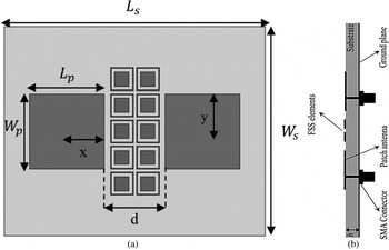
The structure of patch antenna usually consists of a pair of parallel conducting layers separating a dielectric medium. The proposed antenna is designed on an FR4 substrate, with dimensions of 28.75 × 28.75 × 1.6 mm3, permittivity 4.8. The proposed antenna-fed two-coaxial probes are shown in Fig. 1. Feed point is located when 50 Ω resistance occurs. The designed patch antenna has a fractional bandwidth (−10 dB) of 2.41%, which ranges from 6.38 to 6.54 GHz maximum gain is 5.5 dB at the center frequency of 6.46 GHz. In the following section, the design of FSS structure is presented. The input impedance of the patch antenna depends on its geometrical shape and dimensions. The dimensions of the modified antenna are also shown in Table 1. Also all dimensions were calculated from standard formulae as introduced by Balanis [Reference Balanis16].
(a) Top view of two-element antenna array separated by the FSS structure. (b) Side view of two same rectangular patches fed by a coaxial probe.

Dimensions of patch antenna and all dimensions are in mm.

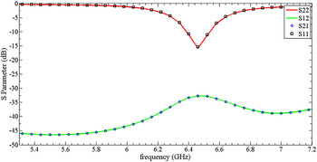
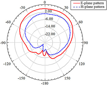
The result of mutual coupling between two patches before placed FSS structure is shown in Fig. 2. This figure shows the S-parameter of arrays antenna without FSS structure. The far-field characteristics of the antenna array are depicted in Fig. 3. This figure shows the simulated E-plane radiation pattern at the 6.4 GHz resonant frequency of the antenna without the FSS structure. The maximum gain is 5.5 dB at the frequency center of 6.4 GHz.
Simulated mutual coupling between patch antennas and input impedance of both antennas.

Simulated far-field characteristics of antenna unit cell in patch antenna array without FSS structure

B) FSS configuration
When periodicity of structure is small compared with the operating wavelength, the operation FSS structure can be described using an equivalent LC circuit model [Reference Balanis16]. The inductor L, results from the current flowing along neighbor patches through narrow lines and the capacitor C is used to model the gap effect between the patches.
The surface impedance equals to the impedance of a parallel resonant circuit and the central frequency of the band gap is calculated as below [Reference Zheng, Fu and Yuan17]:
 $$Z = \displaystyle{{j\omega L} \over {1 - {\omega ^2}LC}},$$
 $${\omega _0} = \displaystyle{1 \over {\sqrt {LC}}}. $$
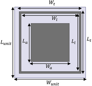
From Fig. 2, it is clear that enhancement of the equivalent capacitance or inductance results in decreasing the resonant frequency and it leads to achieve a compact structure. This study suggests a novel planar compact FSS structure. The schematic of the unit cell of suggested FSS structure is shown in Fig. 4. Dark parts in this figure represent the metallic periodic structure which is etched on a dielectric substrate. The FSS structure was realized by a periodic distribution of metallic elements printed on a dielectric slab. The FSS unit cell was formed of one metallic square loop and one metallic square patch printed on the dielectric substrate. The FSS array was designed on a square dielectric similar to the antennas substrate. The dimensions of FSS unit cell were tabulated in Table 2.
Schematic representation of the unit cell of the suggested FSS structure.

Dimensions of FSS unit cell and all dimensions are in mm.

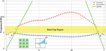
One of the main properties of the FSS structures is the ability to suppress surface waves at frequencies located in the band-gap region compared with another periodic structure such as mushroom-like EBG structure. The FSS structure is easy to fabricate. The drawbacks of patch antenna are solved through the integration of FSS structures. The frequency band gap of the FFS structure can be tuned by changing the geometrical dimensions of FSS unit cell. In this case, the antenna operate frequency is 6.46 GHz. The parameters of the FSS structure are designed in a way that the desired frequency band gap can accommodate the operate frequency of the antenna. To indicate the desired band gap, the dispersion diagram was used because it is an effective tool for considering band-gap characteristics of the FSS structures. The FSS structure printed on antenna substrate. The dispersion diagram in Fig. 5 shown the first band gap includes desired the frequency band.
Simulated dispersion diagram.

The performance of the unit cell is considered by Ansoft HFSS. Periodic boundaries are added on four sides such that an infinite periodic structure could be modeled. The band gap of this structure is 2 GHz which ranges from 5 to 7 GHz.
In Fig. 5, the horizontal axis is named based on the Brillouin zone. Brillouin zone is the smallest indivisible part of the FSS periodic structure. Each of the three point Γ, X, and M is three sides of the triangle Brillouin zone that the calculations of electromagnetic waves have been made on; and the band gap will be achieved [Reference Sakoda18].
III. RESULT AND DISCUSSION
A) Reduction of the number of element
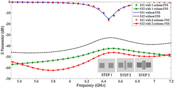
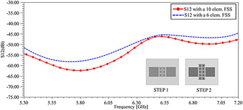
This section investigated the number of FSS elements to obtain lowest mutual coupling. The subjects were told in the INITIAL DESIGN, an appropriate FSS element for the band gap in antenna operating frequency is obtained. Therefore in this section for obtaining the minimum mutual coupling between antenna elements, we focused on the optimal number and the optimal arrangement of FSS elements. The results of the consideration of mutual coupling for antenna without FSS structure, antenna with five FSS elements with single-column, antenna with 10 FSS elements with two-column is shown in Fig. 6. As shown in this figure, the lowest mutual coupling is obtained for 10 FSS elements with two-columns. Then, the mutual coupling is investigated for two another states. The mutual coupling for antenna with six elements FSS with two-column, antenna with 10 FSS elements with two-column is shown in Fig. 7. This figure shows that the mutual coupling for antenna with 10 FSS elements with two-column is lowest. The coupling in this state is less than −46 dB for frequency range of 5.30–7.20 always.
Simulated mutual coupling comparison for the three studied cases: without FSS structure, with one-column FSS, and with two-column FSS. For the FSS dimensions are presented in Table 2.

Simulated mutual coupling comparison for the two studied cases: with a 10-element FSS, and with a six-element FSS for the FSS dimensions are presented in Table 2.

B) Distance effect
As in the previous section, the optimal number of FSS arrays was determined to be 10 FSS elements with two columns. In this section, the effect of increasing distance was examined between the antenna arrays. As shown in Fig. 8, by increasing the distance between the antenna arrays mutual coupling decreased. However, the amount of distance enhancement between the antenna arrays to increase the size of the antenna, and the antenna efficiency was low. It is worth mentioning that, the purpose of this paper is to reduce the mutual coupling between the antenna arrays and keeping both the element separation smaller than λ 0 for grating lobes evasion and the patch antenna size large enough to have a good antenna directivity.
Simulated mutual coupling as a function of the patch separation with (solid lines) and (dashed lines) without FSS. Distanced is increased by a step of 0.05λ from 0.5λ to 0.065λ. FSS dimensions are the same for all curves, and for FSS dimensions are presented in Table 2.

C) Experimental results
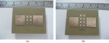
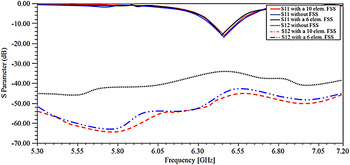
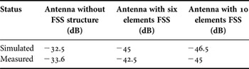
At the end two-sample studied antennas were fabricated. Figure 9 shows the antennas that were fabricated. The results of measuring S11 and S12 for the antenna arrays without FSS structure, antenna with 10 FSS elements with two-column and antenna with six elements FSS with two-column is shown in Fig. 10. This study confirms the results that were obtained by simulation, and also shows that the optimum number of FSS arrays is 10 arrays, and the optimal arrangement for FSS arrays, is two columns. Finally, Table 3 shows the mutual coupling between two-element patch antenna array with and without FSS structures in antenna resonant frequency.
Photographs of the fabricated planar periodic structure (a) with six elements FSS and (b) with 10 elements FSS.

Measured prototype without FSS and with two different FSS (with six and 10 elements FSS). Distance between edges of patch antennas is 23.25 mm and parameters of the FSS are presented in Table 2.

Mutual coupling between two-element patch antenna array with and without FSS structures in antenna resonant frequency.

IV. CONCLUSION
The fundamental aim of this research was to explore the potential effect of mutual coupling between two-element patch antenna arrays, where the periodic FSS structure was placed between the elements. Periodic structures such as FSS can help in the reduction of mutual coupling using their ability of suppressing surface waves propagation in a given frequency range. The properties of FSS were verified using band-gap analysis. Compared with the other decoupling techniques, the suggested decoupling design provides a good coupling suppression level for closely spaced patches antenna and involves an easy and straightforward fabrication process. The proposed configuration affords an improvement in mutual coupling by 14 dB (measured value) with a reduced edge-to-edge spacing of 23 mm. According to the results, if the number of FSS elements is further mutual coupling reduced. However, more than 10 FSS elements are caused to enlarge the size of the antenna. The 10 elements are optimal.
ACKNOWLEDGEMENTS
The authors would like to thank the faculty of Semnan University to support this work.
 Ehsan Beiranvand was born in Khorramabad, Iran, in 1988. He received the B.S. degree in Shahid Chamran University, Ahvaz, Iran, in 2011. Currently, he is working toward the M.S. degree in Communication Engineering from Semnan University. His current research interests are in FSS structure and Fabry–Perot antenna.
 Majid Afsahi received the B.Sc. degree in Electrical and Electronics Engineering from Tehran University, Iran, in 1991, the M.S. degree in Electrical Engineering from Amirkabir University of Technology in 1993, and the Ph.D. degree in Electrical and Electronics Engineering Iran University of Science and Technology, Iran, in 2010. He has taught and done research at Shahid Bahonar University of Kerman on Antennas and RF/microwave passive structures and he has worked in Telecommunication Company of Iran on cellular and RF systems. In 2010, he joined the Department of Electrical and Computer Engineering, Semnan University Semnan, Iran, as an Assistant Professor. His research interests are in the area of radio wave propagation in conventional and metamaterial media, antenna and RF/microwave passive components, and numerical methods in electromagnetic engineering.
 Vahid Sharbati was born in Gorgan, Iran, in 1986. He received the B.S. degree in Electronic Engineering from Hadaf Institute of Higher Education, Sari, Iran, in 2009. Currently, he is working toward the M.S. degree in Communication Engineering from Semnan University. His current research interest is reconfigurable microstrip antenna for cognitive radio applications.