Introduction
The role of charge transport layer is one of the most important parameters in the field of solar cells[Reference Litzov and Brabec1, Reference Lattante2] and photodetectors.[Reference Baeg, Binda, Natali, Caironi and Noh3, Reference Pal, Robel, Mohite, Laocharoensuk, Werder and Klimov4] Multiple materials are used as a charge transport layer among which ZnO,[Reference Pal, Robel, Mohite, Laocharoensuk, Werder and Klimov4] TiO2,[Reference Pal, Robel, Mohite, Laocharoensuk, Werder and Klimov4] Cs2CO3,[Reference Liao, Chen, Xu, Li and Yang5] and Nb2O5[Reference Wiranwetchayan, Liang, Zhang, Cao and Singjai6] are the mostly used as an electron transport layer (ETL).[Reference Lattante2] While the materials such as PEDOT:PSS,[Reference Ionescu-Zanetti, Mechler, Carter and Lal7, Reference Kemerink, Timpanaro, de Kok, Meulenkamp and Touwslager8] MoOx,[Reference Girotto, Voroshazi, Cheyns, Heremans and Rand9] NiO,[Reference Caruge, Halpert, Bulović and Bawendi10] WO3,[Reference Kemerink, Timpanaro, de Kok, Meulenkamp and Touwslager8] and V2O5[Reference Zilberberg, Trost, Meyer, Kahn, Behrendt, Lützenkirchen-Hecht, Frahm and Riedl11] are used as a hole transport layer (HTL). Wide and direct band gap metal–oxide semiconductors such as ZnO and TiO2 are the most viable option for ETL due to their inherent n-type nature, high transparency in the visible region, and suitability for widespread deposition techniques from physical to chemical deposition methods. However, the solution-based deposition technique is considered to be the most cost-effective and simplest method for large area nanoelectronics.[Reference Tsay, Fan, Chen and Tsai12] Furthermore, ZnO is widely investigated due to its low cost,[Reference Liu, Sakurai and Aono13] large abundance,[Reference Liu, Sakurai and Aono13, Reference Wang14] and consistent nature of being n-type, whereas TiO2 varies between semiconductor to insulator depending upon the phase of the TiO2 thin film or nanocrystal.[Reference Kumar, Kumar, Rawat, Kumar, Sharma, Pal and Jit15–Reference Rawat, Somvanshi, Kumar, Kumar, Kumar and Jit18] Similarly, MoOx is mostly preferred HTL[Reference Litzov and Brabec1, Reference Lattante2] the involvement of MoOx layer as HTL provides greater air stability to the fabricated device structure compared with other HTL counterparts.[Reference Chambon, Derue, Lahaye, Pavageau, Hirsch and Wantz19] However, for the deposition of MoOx thin-film thermal evaporation is the most used technique.[Reference Lattante2] MoOx deposited via thermal evaporation are very sensitive toward the temperature and deteriorate with annealing temperature.[Reference Chambon, Derue, Lahaye, Pavageau, Hirsch and Wantz19] This limitation of MoOx reduces the quality of the solar cells and photodetectors, as the improvement in morphology is important for the interfaces and the heterojunctions.[Reference Yadav, Pandey and Jit20] The morphology of the deposited thin film can be easily controlled, modified, or improved by annealing of the respective thin film under suitable temperature and environment.[Reference Kumar, Kumar, Rawat, Kumar, Sharma, Pal and Jit15, Reference Yadav, Pandey and Jit20–Reference Yadav, Periasamy and Jit23] Girotto et al.[Reference Girotto, Voroshazi, Cheyns, Heremans and Rand9] prepared MoO3 based solar cell using both solution processing and thermal evaporation and also prepared a device using PEDOT:PSS. They[Reference Girotto, Voroshazi, Cheyns, Heremans and Rand9] have found that performance of solution-processed MoO3 is equivalent to the thermal evaporation processed MoO3 and outperform the PEDOT:PSS-based solar cell device.
In this work, we have fabricated and characterized the MoOx/ZnO quantum dots (QDs) heterojunction on an ITO-coated glass substrate using low-cost solution-processed technique. The electrical and optical properties of MoOx/ZnO QDs are analyzed for thermally grown and solution-processed MoOx. Further, the effect of heat treatment at 280 °C post-fabrication of the device on the electrical properties of the devices is also analyzed for the thermally grown and solution-processed MoOx over ZnO QDs thin film.
Experimental details
The fabrication of device starts from depositing the ZnO QDs thin film on the ITO-coated glass substrates cleaned thoroughly by using alcanox, deionized water, acetone, and isopropanol subsequently, and then dried at 90 °C for 15 min as reported elsewhere.[Reference Kumar, Kumar, Rawat, Kumar, Sharma, Pal and Jit15] The used chemicals were acquired from MERK-Chemical Limited, Mumbai, India and Sigma-Aldrich and used without any further purification. The fabrication of the device is described in the following three steps.
Preparation of ZnO QDs
The synthesis of ZnO QDs was performed using the hot-injection method already reported elsewhere.[Reference Kumar, Kumar, Rawat, Kumar, Sharma, Pal and Jit15] The prepared solution was filtered using the polyvinylidene fluoride membrane (0.22 µm) to remove the large and unreacted materials from the solution to enhance the surface uniformity of the thin film. Furthermore, the filtered colloidal ZnO QDs was deposited on the cleaned patterned ITO-coated glass substrate using spin coating (SPM-150LC TSE- system GmbH, Germany). The prepared sample is placed in a pre-heated oven at 200 °C for 30 min under ambient environment. The monoethanolamine (MEA) used for the preparation of ZnO QDs defines the lower limit of temperature as the evaporation temperature of MEA is ~160–190 °C. The process of spin-coating and heating is iterated till the desired thickness of ~ 40 nm is achieved measured by Reflectometer (F-20 Thin Film UV Analyzer, Filmetrics). Afterward, the ZnO QDs thin film is annealed at 250 °C under the ambient environment for 30 min. The prepared samples are used with solution-processed MoOx and thermally evaporated MoOx to analyze the effect of heat treatment.
Preparation of MoOx solution
MoOx solution is prepared using the technique specified by Girotto et al.[Reference Girotto, Voroshazi, Cheyns, Heremans and Rand9] The 1 M solution of MoO2 powder is stirred with H2O2 for ~2 h at 80 °C under the ambient environment and then allowed to cool down for 24 h to obtain a clear yellow liquid. Acetylacetone is further used to modify the viscosity and concentration of the solution. The concentration of H2O2 defines the quality of the solution; excess H2O2 makes the solution stable for a long duration, while it changes to dark-blue solution due to the insufficient conversion of MoO3 into MoO3(OH)(OOH) under the deficiency of H2O2.[Reference Girotto, Voroshazi, Cheyns, Heremans and Rand9] The prepared solution is spin-coated on an ITO/ZnO QDs substrate, and then annealed at 270 °C. The process is repeated to achieve the thickness of 30–35 nm measured using Reflectometer (F-20 Thin Film UV Analyzer, Filmetrics).
Device fabrication
Thermal evaporation (vacuum evaporation) is used for the deposition of high-purity Ag (99.99%) and MoOx using HHV, FL400 SMART COAT 3.0 A. Thermal deposition of MoOx was performed on the ITO/ZnO QDs to achieve a thickness of ~30 nm. Afterward, the thermal deposition of Ag was performed on the solution and thermally prepared ITO/ZnO QDs/MoOx using a shadow mask technique, and the thickness of ~50 nm is achieved. Thermal deposition of both the materials (MoOx and Ag) was performed at a vacuum of ~10−6 bar at the variable rate (for first 5 nm 0.1 Å/s, for 5–20 nm 0.5 Å/s, and for 20 nm onwards 1 Å/s). The thickness of the deposited thin film and the rate of evaporation are monitored using digital thickness monitor (INFICON model no. SQM-160) attached to the coating unit. Furthermore, the complete device is heated at 280 °C for 30 min under the ambient environment after the one set of results are obtained as discussed in further sections. The effect of post-heat treatment on the Ag electrodes is shown in the Supplementary Material.
Results and characterization
Structural characterization
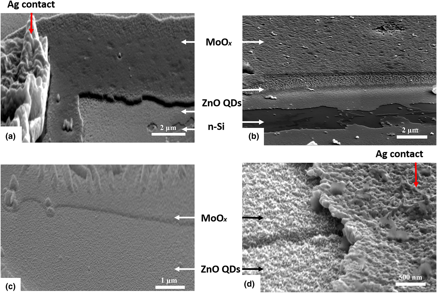
The high-resolution scanning electron microscopy (HRSEM: SUPRA 40, Zeiss) image of the complete device structure with solution-processed and thermally grown MoOx is performed before heat treatment of the complete device and after heat treatment of the complete device at 280 °C under the ambient environment for 30 min as shown in Fig. 1. The HRSEM of the solution-processed MoOx-based diode shows the stability of the device as the layers are distinguished after the heat treatment and indicates separable interface between MoOx and ZnO QDs as shown in Figs. 1(a) and 1(b). Similarly, HRSEM of the diode with thermally evaporated MoOx is performed and shown in Figs. 1(c) and 1(d). The device after heat treatment shows the continuous interface between thermally grown MoOx and ZnO QDs, which may be due to the diffusion of MoOx into the ZnO QDs shown in Fig. 1(d). The morphology of as-grown ZnO QDs is also analyzed using transmission electron microscopy (TEM: TECNAI G2 20 TWIN) image shown in Supplementary Fig. S1 and diffraction pattern is shown in Fig. S2. The detailed analysis of the ZnO QDs size and orientation is reported in our previous work.[Reference Kumar, Kumar, Mukherjee, Rawat, Kumar, Pal and Jit24] The effect of heat treatment on the Ag electrode is shown for both devices in the Supplementary Figs. S3–S6. Furthermore, the annealing of the thin films greatly improves the morphology and interface characteristics of the devices and materials. Thermally deposited MoOx does not show any grains in Fig. 1(c), but after the heat treatment of the complete device the grain boundaries are visible leading to the crystallization of the MoOx thin film shown in Fig. 1(d). In the case of solution-processed MoOx, annealing of the film is performed at 270 °C under ambient environment for 30 min. The annealing of solution-processed MoOx crystallizes the MoOx film shown in Fig. 1(a).
HRSEM image of (a) solution-processed MoOx-based device before annealing at 280 °C, (b) solution-processed MoOx-based device after annealing at 280 °C, (c) thermally grown MoOx-based device before annealing at 280 °C, and (d) thermally grown MoOx-based device after annealing at 280 °C.

Optical characterization
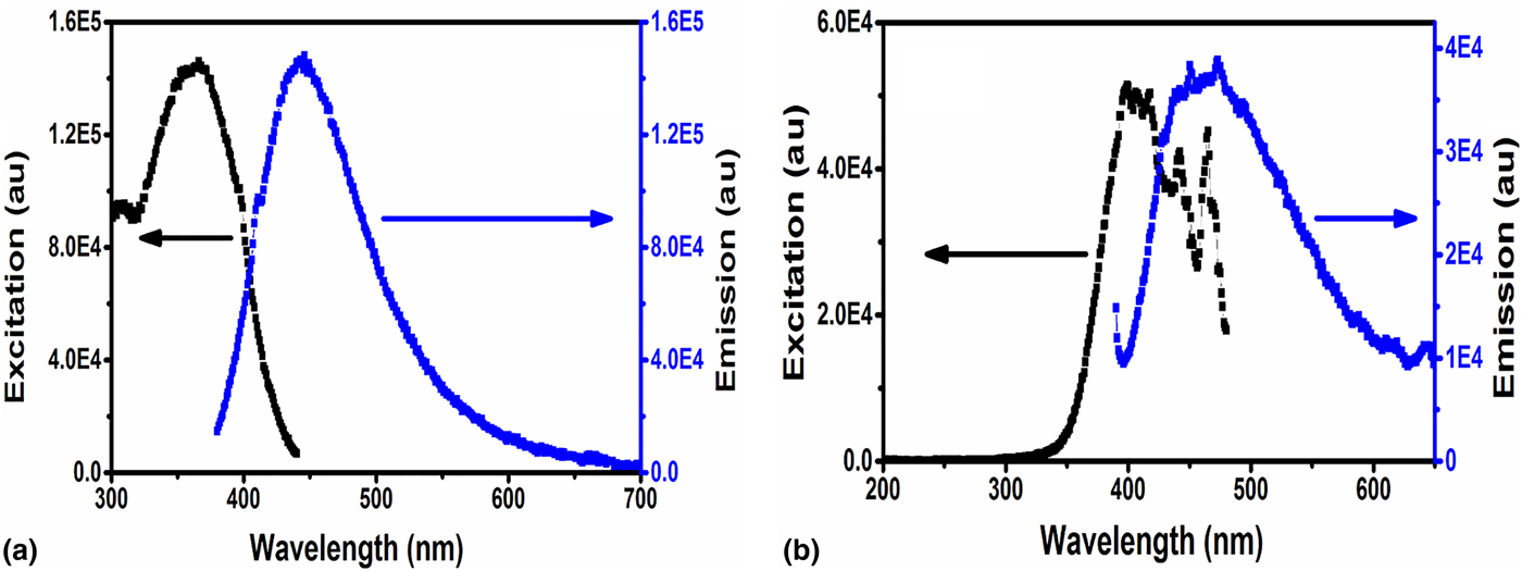
The study of optical properties of MoOx and ZnO QDs is analyzed in this section. The photoluminescence excitation (PLE) and emission spectrum of ZnO QDs and MoOx are shown in Figs. 2(a) and 2(b), respectively. The PLE spectrum of ZnO QDs shows a peak at 365 nm (3.39 eV), the curve of absorption spectra is fitted to match the wavelength axis. The peak of PLE spectrum for MoOx is obtained at ~400 nm, and the same is also shown in Figs. 2(a) and 2(b). The PL spectrum of the material provides great details about the monodispersity of the nanocrystals, quality of the film or synthesized material, and interface defects if any. The PL spectrum of ZnO QDs shown in Fig. 2(a) shows the narrow-band emission spectrum with a full-width at half-maximum (FWHM) of 72 nm. The selectivity of ZnO QDs PL indicates the high-quality and monodispersity of the ZnO QDs. The PL of QDs can be treated as a surface-dependent phenomenon due to the dependence of band gap upon the particle size of the QDs.[Reference Klimov25] The PL spectrum of MoOx shown in Fig. 2(b) has the FWHM of 125 nm and shows no trailing edges indicates that the MoOx are free from any surface defects. The involvement of surface defects increases the charge-trapping sites.
(a) Photoluminescence (PL) excitation and emission spectrum of colloidal ZnO QDs solution and (b) PL excitation and emission spectrum of MoOx-solution.

Electrical characterization
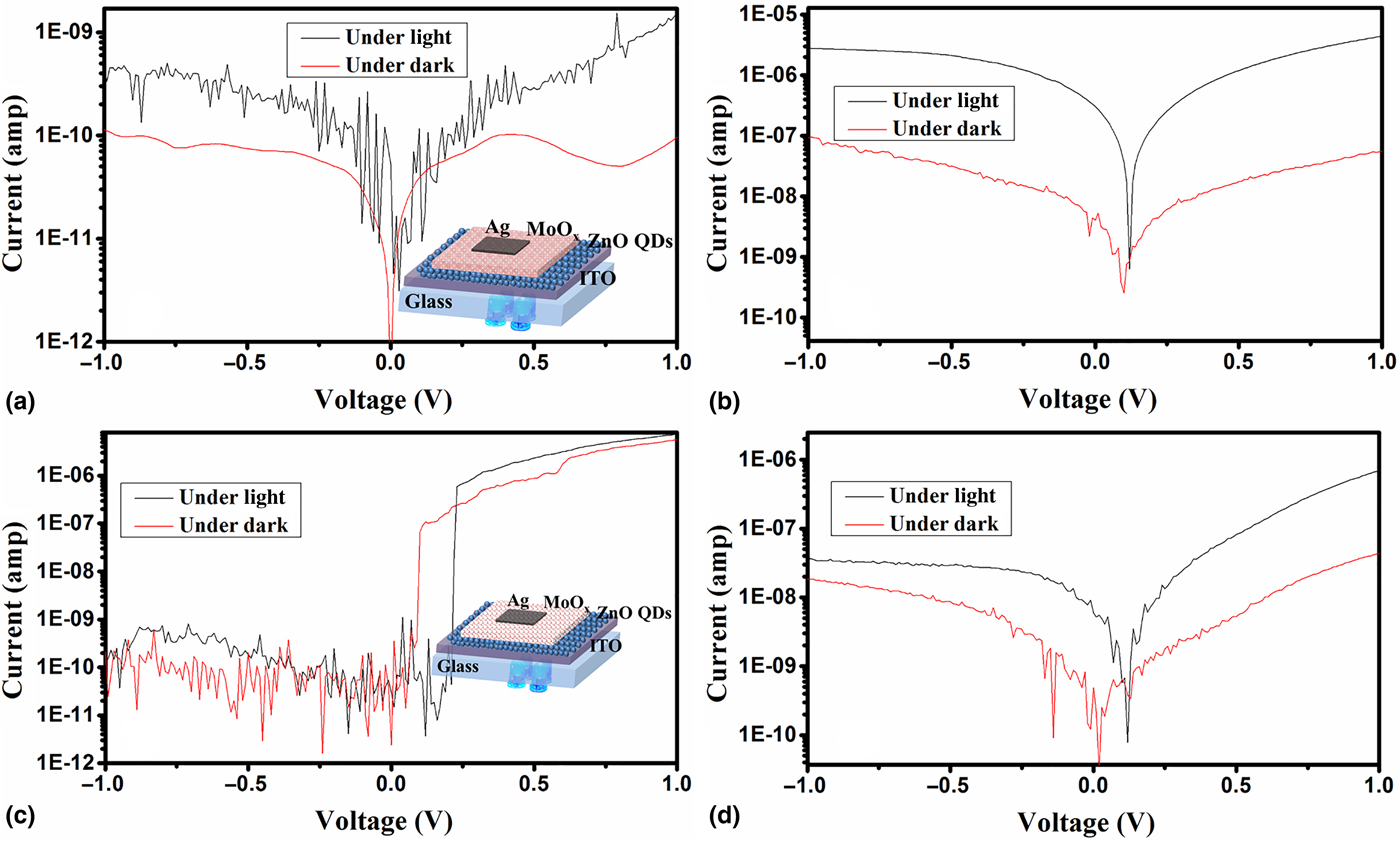
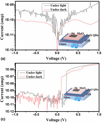
The current versus voltage (I–V) relationship for the devices with MoOx grown by solution processing and thermal evaporation are shown in Fig. 3, measured using Keysight B1500A from −1 to +1 V. The device under study for MoOx grown by solution processing and thermal evaporation is also shown in the inset of Figs. 3(a) and 3(c), respectively. The I–V curve is plotted under the dark and under the illumination of UV light (UV LED source with an optical power density of 800 µW/cm2 at 365 nm). The effect of heat treatment on the complete device is evident in both devices as the dark current (noise current) increases with the annealing. The solution-processed MoOx-based device shows superior photoresponse after heat treatment compared with the device without heat treatment. Furthermore, the stability of the photocurrent is also observed in Fig. 3(b) compared with Fig. 3(a) and the contrast ratio (I ph/I dark) of the device enhanced from 3.88 to 38.72 at an applied bias of −1 V. The thermally grown MoOx-based device shows deterioration in rectifying nature of the device and the noise current is increased by ratio of greater than ~100 times shown in Figs. 3(c) and 3(d). This deterioration of the device is due to the diffusion of MoOx into the ZnO QDs, which varies the barrier between the ZnO QDs and MoOx from graded to the linear junction. The photoresponse of the devices can be compared using the responsivity of the device calculated using:
 $${\mathop{\rm Re}\nolimits} (v,\lambda ) = \displaystyle{{\mathop I\nolimits_{{\rm ph}} (v,\lambda )} \over {\mathop P\nolimits_{{\rm opt}} (\lambda )}},$$
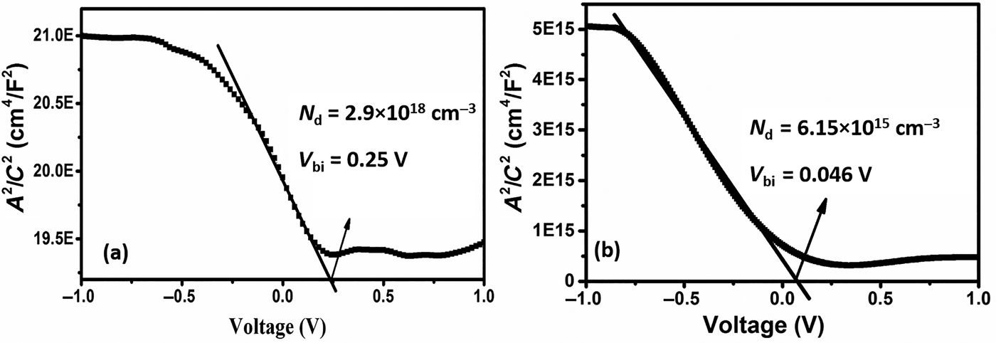
where I ph is the photocurrent obtained at a bias of V volts at wavelength λ. The P opt is the optical power density of the light source measured at wavelength λ using the power meter (PM100D, Thorlabs). The measured responsivity of the devices with and without heat treatment under the illumination of UV LED at an applied bias of −1 V are indicated in Table I. The A 2/C 2 versus voltage curve for solution-processed and thermally grown MoOx-based device after heat treatment is shown in Fig. 4. The heterojunction between MoOx and ZnO QDs is assumed to be a Schottky junction, and therefore most of the depletion region will reside in ZnO QDs thin film. The curves shown in Fig. 4 can be interpreted as
 $$\displaystyle{{A^2} \over {C^2}} = \displaystyle{2 \over {q\varepsilon}} \left( {\displaystyle{{\phi - V} \over {N_{\rm d}}}} \right),$$
where N d is the donor concentration in n-type layer, ε is the effective dielectric constant of the ZnO QDs film, q is the electron charge, and ϕ is the built-in potential. From the projected intersection of capacitance curve in voltage axis we find the value of built-in potential and found to be 0.25 and 0.046 V for solution-processed and thermally grown MoOx-based device, respectively. Thus, the low built-in potential shown by a diode (for thermally grown MoOx) indicates the junction between ZnO QDs and MoOx is not abrupt but the linear in nature. The ideality factor of the diodes are also calculated and found to be 3.85 and 6.14 for solution-processed and thermally grown MoOx-based device, respectively. The ideality factor defines the quality of the diode (junction). Ideally, the value of ideality factor should be equal to 1, but due to interface defects this result deviates from 1 and tends to increase >1. The high value of ideality factor 6.14 also indicates the low quality of junction formed between thermally grown MoOx and ZnO QDs.
Logarithmic current–voltage curve under light and dark condition for (a) solution-processed MoOx-based diode without annealing, (b) solution-processed MoOx-based diode after annealing, (c) thermally grown MoOx-based diode without annealing, and (d) thermally grown MoOx-based diode with annealing. The complete device structure of the solution-processed and thermally grown MoOx are shown in the inset of (a) and (c), respectively.

A 2/C 2 versus voltage curve for (a) solution-processed MoOx-based diode and (b) thermally processed MoOx-based diode.

Responsivity of the fabricated devices under the optical power density of 800 µW/cm2 at 365 nm.

Conclusion
In this work, solution-processed and thermally grown MoOx is used to fabricate a heterojunction with ZnO QDs and effect of treatment is analyzed for electrical and optical properties possibly for the first time. The effect of heat treatment on the device performance is measured for I–V, responsivity, and contrast ratio. The solution-processed MoOx-based diode shows stable results after heat treatment, but the thermally grown MoOx-based diode deteriorates. Thermally grown MoOx-based device looses the rectifying behavior and the noise current increases 100 times with the heat treatment. Further, the low value of V bi (0.046 V) and high value of ideality factor (6.14) after heat treatment indicates the poor quality of junction between thermally grown MoOx and ZnO QDs. The responsivity of the solution-processed MoOx-based diode after heat treatment is found to be 3.93 mA/W at 365 nm, which is ~7198 times higher than solution-processed MoOx without heat treatment.
Supplementary material
The supplementary material for this article can be found at https://doi.org/10.1557/mrc.2017.68.