Introduction
Advancements in magnetic detection and imaging have contributed immensely to a wide range of scientific areas from fundamental physics and chemistry to practical applications such as the data storage industry and medical science. One classic example is nuclear magnetic resonance,Reference Rabi, Zacharias, Millman and Kusch 1 , Reference Bloch 2 which has led to powerful applications such as magnetic resonance imagingReference Mansfield 3 (MRI). Over the past few decades, many advanced magnetic imaging schemes have been developed, including magnetic force microscopy,Reference Martin and Wickramasinghe 4 scanning Hall probe microscopy,Reference Chang, Hallen, Harriott, Hess, Kao, Kwo, Miller, Wolfe, van der Ziel and Chang 5 superconducting interference devices,Reference Kirtley, Ketchen, Stawiasz, Sun, Gallagher, Blanton and Wind 6 and magnetic resonance force microscopy.Reference Zuger and Rugar 7 However, these techniques are often limited by operating conditions such as the need for cryogenic temperatures and/or high vacuum, hindering their use in imaging systems that require ambient conditions.
Recently, negatively charged nitrogen-vacancy (NV) color centers in diamond have been proposed as a promising system for nanoscale magnetic field sensing.Reference Taylor, Cappellaro, Childress, Jiang, Budker, Hemmer, Yacoby, Walsworth and Lukin 8 – Reference Degen 11 It has been shown, both experimentally and theoretically, that NV centers offer excellent magnetic field sensitivities.Reference Taylor, Cappellaro, Childress, Jiang, Budker, Hemmer, Yacoby, Walsworth and Lukin 8 , Reference Maze, Stanwix, Hodges, Hong, Taylor, Cappellaro, Jiang, Dutt, Togan, Zibrov, Yacoby, Walsworth and Lukin 10 Moreover, since NV centers are atomic-sized point defects and can be localized in direct proximity to a diamond surface, they can be brought to within a few nanometers of magnetic samples, allowing for nanometric spatial resolution. These sensing capabilities are maintained under ambient conditions (room temperature and atmospheric pressure) and can, in principle, work in a liquid environment, which is crucial for biological imaging. Over the past few years, these properties have led to rapid progress in developing NV-based magnetometers. In this review article, we cover two recently developed methods to realize NV-based magnetometers: Scanning single NV magnetometers capable of detecting a single Bohr magneton at the nanoscale, and ensemble NV wide-field imaging, enabling enhanced magnetic field sensitivities and data acquisition speeds.
Magnetic field sensing with NV centers
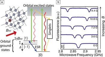
The NV center is a point defect in diamond consisting of a substitutional nitrogen with a vacancy in its nearest neighbor lattice site ( Figure 1 a). The negatively charged state forms a spin triplet in the orbital ground state. The crystal field splits these spin sublevels, resulting in the m s = 0 state in the lowest energy state, and the m s = ±1 sublevels lifted by 2.87 GHz. This crystal field splitting quantizes the spin states along the N–V symmetry axis, so that in the presence of a weak external magnetic field, the m s = ±1 sublevels will have an energy splitting that is proportional to the projection of the field along the N–V axis. This Zeeman splitting can be used to isolate an effective spin-1/2 system (for instance, m s= 0 and +1 states). The population of this spin-1/2 system can be read out and initialized optically via spin-dependent fluorescence and optical pumping, respectively. These optical readout and initialization schemes, along with coherent microwave manipulation of the spin’s state, allow for full access to the NV center’s spin states.
(a) Level diagram of a single nitrogen-vacancy (NV) center in diamond. A NV center emits fluorescence (red) under off-resonant optical excitation (green). When the NV center’s spin state is m s = 1 or –1, once optically excited, it decays through metastable singlet states to m s = 0. This leads to optical initialization and spin-dependent fluorescence, which can be used to read out the probability of the spin state. ESR, electron spin resonance. (b) Optically detected ESR spectra as a function of magnetic field along the NV axis. The NV’s spin triplet has a zero magnetic field splitting (Δ ∼2.87 GHz), and m s = 1 and –1 states are degenerate, resulting in a single spin resonance frequency. In an external field, m s= 1 and –1 states split proportional to the field projected along the N–V axis, resulting in two spin resonance frequencies.

Magnetic field sensing with NV centers is based on this Zeeman splitting of the NV’s spin states,Reference Taylor, Cappellaro, Childress, Jiang, Budker, Hemmer, Yacoby, Walsworth and Lukin 8 – Reference Maze, Stanwix, Hodges, Hong, Taylor, Cappellaro, Jiang, Dutt, Togan, Zibrov, Yacoby, Walsworth and Lukin 10 as the m s = ±1 state’s energy splitting directly reflects the magnetic field projection along the N–V axis. The NV center’s Zeeman energy shift can therefore be read out optically. Optically detected electron spin resonance (ESR) spectra,Reference Gruber, Drabenstedt, Tietz, Fleury, Wrachtrup and Borczyskowski 12 for instance, can be used for magnetic field sensing, as spin resonance frequencies shift proportional to external magnetic fields (Figure 1b).
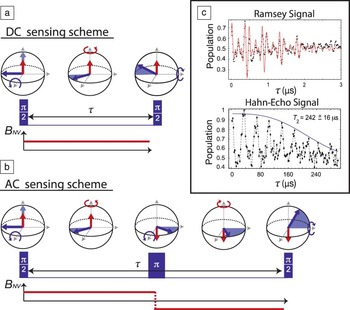
A well-established methodology to determine Zeeman shifts, widely used in spin-based magnetometers such as atomic vapor cells, is to monitor changes in spin precession.Reference Budker, Gawlik, Kimball, Rochester, Yashchuk and Weis 13 This type of approach uses a Ramsey-type measurement sequence.Reference Taylor, Cappellaro, Childress, Jiang, Budker, Hemmer, Yacoby, Walsworth and Lukin 8 When the spin’s state is prepared in an equal superposition state, the spin rotates at a rate proportional to the local magnetic field B. As a result, during a fixed evolution time τ, the phase of the spin state ϕ accumulates by an amount γBτ (where γ is the gyromagnetic ratio of an electron spin), reflecting the magnetic field B ( Figure 2 a). This accumulated phase is converted to a probability distribution between the m s = 0 and m s= ±1 states that can be read out via spin-dependent fluorescence. In the limit of small magnetic fields, the corresponding shot-noise-limited magnetic field sensitivity (minimally detectable field within 1 s acquisition time) is described by
 $${\rm{\delta }}B_{{\rm{opt}}} \~{1 \over {\rm{\gamma }}} \cdot {{\sqrt {2\left({C_0 + C_1 } \right)} } \over {\left({C_0 - C_1 } \right)}} \cdot {1 \over {\sqrt {N \cdot {\rm{\tau }}_{{\rm{opt}}} } }},$$
(a) Magnetic field detection scheme with electron spin resonance pulse sequences. Measurement of static magnetic field is based on a Ramsey pulse sequence. The measurement starts with preparing a NV spin’s state in an equal superposition of m s = 0 and m s = 1 (or –1) by applying π/2-pulse. During a free evolution time τ, phase is accumulated in proportion to the field. The second π/2-pulse converts the phase to the probability distribution of the NV’s spin states, which can then be measured through spin-dependent fluorescence. (b) An echo-based (Hahn) pulse sequence can improve the magnetic field sensitivity, provided that it measures an AC magnetic field with its period matched to the total free evolution time. It allows for a longer free evolution time by prolonging the coherence time. (c) Electron spin coherence times of an NV center in high-purity diamond.Reference Childress, Gurudev Dutt, Taylor, Zibrov, Jelezko, Wrachtrup, Hemmer and Lukin 32 The coherence time in the Hahn-echo signal (242 μs) is two orders of magnitude longer than the coherence time of the Ramsey signal (∼2 μs). Adapted with permission from Reference Reference Childress, Gurudev Dutt, Taylor, Zibrov, Jelezko, Wrachtrup, Hemmer and Lukin32. © 2006 American Association for the Advancement of Science.

where C 0 and C 1 are the numbers of photons collected per one measurement shot per one NV in the spin states m s = 0 and m s = 1, respectively, N is the number of NV centers participating in the measurement, and τopt is the optimal evolution time, which would normally be determined by the NV’s phase coherence time.
The coherence of NV centers is limited by the surrounding spins in diamond arising from paramagnetic defects and Reference Budker, Gawlik, Kimball, Rochester, Yashchuk and Weis 13 C nuclear spins (1.1% abundance). The coherence time, however, can be extended by orders of magnitude using decoupling sequences such as a Hahn-echo sequence (Figure 2b).Reference Taylor, Cappellaro, Childress, Jiang, Budker, Hemmer, Yacoby, Walsworth and Lukin 8 , Reference de Lange, Ristè, Dobrovitski and Hanson 14 Using these techniques, often referred to as AC sensing schemes, a NV center becomes sensitive only to time-varying magnetic fields whose duty cycles are matched to the decoupling sequence used,Reference Taylor, Cappellaro, Childress, Jiang, Budker, Hemmer, Yacoby, Walsworth and Lukin 8 therefore requiring modulation of targeted magnetic sources. For detecting paramagnetic spins, this can be achieved by conventional resonant driving methods. A unique property of NV centers compared to other solid-state spin qubit systems, is that the long coherence times of the spins are maintained even at room temperature. Using the AC sensing scheme, it has been shown that a single NV center in high purity (i.e., low defect concentration) diamond is already capable of 30 nT Hz–1/2 sensitivityReference Maze, Stanwix, Hodges, Hong, Taylor, Cappellaro, Jiang, Dutt, Togan, Zibrov, Yacoby, Walsworth and Lukin 10 and can achieve 4.3 nT Hz–1/2 by isotopic engineeringReference Balasubramanian, Neumann, Twitchen, Markham, Kolesov, Mizuochi, Isoya, Achard, Beck, Tissler, Jacques, Hemmer, Jelezko and Wrachtrup 15 under ambient conditions (i.e., room temperature and atmospheric pressure).
A critical advantage of magnetic sensing with NV centers is that they are atomic-sized point defects in solids. Nanoscale magnetic imaging generally requires the sensor’s close proximity to the sample of interest in addition to small detection volume of the sensor, since the magnetic field from individual spins, which are the fundamental building blocks of magnetism, falls off as the separation cubed. It also means that bringing the sensor closer to the sample places it in a stronger field and therefore results in faster detection times. Fulfilling these requirements is a challenging problem in other spin precession–based magnetometers; for example, an atomic vapor cell magnetometer has recently been demonstrated with 70 fT Hz–1/2 sensitivity,Reference Shah, Knappe, Schwindt and Kitching 16 but its size, and therefore the spatial resolution, remained on the order of a millimeter. Furthermore, since the magnetic field of a single electron spin at this distance is reduced to zeptotesla (10–21 T), detecting it with the vapor cell is impossible. However, for a single NV center, the crystal lattice naturally provides a tight and stable trapping of NV centers’ electronic wave functions within only a few angstroms. Furthermore, it has been recently reported that NV centers can be formed within 5 nm of the diamond surface, while maintaining coherence times longer than 100 μs.Reference Ohno, Heremans, Bassett, Myers, Toyli, Jayich, Palmstrom and Awschalom 17 This combination of tight confinement and nanometer-scale proximity to the diamond surface suggests that it is feasible to bring NV centers to within a few nanometers of the sample. Since the magnetic field of an electron spin at this distance is roughly in the microtesla range, it is possible to detect it, provided that the NV center’s sensitivity is maintained as in References Reference Maze, Stanwix, Hodges, Hong, Taylor, Cappellaro, Jiang, Dutt, Togan, Zibrov, Yacoby, Walsworth and Lukin10 and Reference Balasubramanian, Neumann, Twitchen, Markham, Kolesov, Mizuochi, Isoya, Achard, Beck, Tissler, Jacques, Hemmer, Jelezko and Wrachtrup15.
In addition, these solid-state aspects of NV centers are also advantageous for implementing ensemble magnetometers for higher magnetic field sensitivity. For instance, well-established techniques for defect engineering, such as ion-implantationReference Rabeau, Reichart, Tamanyan, Jamieson, Prawer, Jelezko, Gaebel, Popa, Domhan and Wrachtrup 18 and delta-doping (the formation of atomically thick doped layers),Reference Ohno, Heremans, Bassett, Myers, Toyli, Jayich, Palmstrom and Awschalom 17 can be readily applied to create high density NV ensembles within a thin layer at the surface of a bulk diamond chip (see the article by Wrachtrup et al. in this issue). These highly concentrated ensembles of NV centers could boost magnetic field sensitivity while maintaining microscopic sensing volumes.
Scanning magnetometry with a single NV center
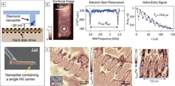
As discussed previously, maintaining a short separation distance between the sensing NV centers and the sample is crucial for nanoscale magnetic imaging. The first nanoscale NV magnetometer was implemented using commercially available diamond nanocrystals hosting a single NV center grafted at the apex of an AFM tipReference Balasubramanian, Chan, Kolesov, Al-Hmoud, Tisler, Shin, Kim, Wojcik, Hemmer, Krueger, Hanke, Leitenstorfer, Bratschitsch, Jelezko and Wrachtrup 9 ( Figure 3 a–b). The size of the diamond nanocrystals, nominally 40 nm in diameter, ensured proximity of the NV center to the sample and a corresponding magnetic spatial resolution within a few tens of nanometers. Magnetic images could then be acquired by scanning the NV center with respect to the sample while recording the NV’s spin-dependent fluorescence in response to the sample’s local magnetic field. In this first demonstration, the spatial profile of the magnetic field from a magnetic nanostructure was imaged by monitoring the NV center’s fluorescence while external microwaves were continuously applied with a fixed frequency (Figure 3c). The dark resonance line appearing in the image corresponds to the positions where the magnetic field from the sample shifts the NV’s ESR frequency to coincide with the microwave drive frequency.
Nanoscale magnetometry with a scanning single nitrogen-vacancy (NV) center. (a) Schematic of scanning NV magnetometry. Adapted with permission from Reference Reference Maletinsky, Hong, Grinolds, Hausmann, Lukin, Walsworth, Loncar and Yacoby19. © 2012 Nature Publishing Group. (b) Schematic of an atomic force microscopy (AFM) probe with diamond nanocrystal containing a single NV center. (c) Spatial image of a magnetic field profile from a magnetic structure acquired by a diamond nanocrystal probe. Adapted with permission from Reference Reference Balasubramanian, Chan, Kolesov, Al-Hmoud, Tisler, Shin, Kim, Wojcik, Hemmer, Krueger, Hanke, Leitenstorfer, Bratschitsch, Jelezko and Wrachtrup9. © 2008 Nature Publishing Group.

More recently, an alternative method has been developed to improve the sensitivity of scanning NV magnetometers. This scheme is based on monolithic diamond nanopillars containing single NV centers, fabricated from high-purity, single-crystalline diamond.Reference Maletinsky, Hong, Grinolds, Hausmann, Lukin, Walsworth, Loncar and Yacoby 19 The fabrication procedure consists of two e-beam lithography and oxygen plasma etching steps on each side of the high-purity diamond membrane, one for the nanopillar and the other for the cantilever. The high quality of bulk diamond materials yields longer coherence times compared to commercial diamond nanocrystals. Moreover, nanopillars are designed to support efficient optical wave-guiding of the NV’s fluorescence by more than a factor of 5 compared to conventional far-field collection, while requiring an order of magnitude less of optical excitation power (see the article by Loncar and Faraon). This combination of long coherence time and increased photon collection efficiency results in excellent magnetic field sensitivity. For these devices, NV centers are created within a few tens of nanometers of the tip surface via nitrogen ion implantation,Reference Rabeau, Reichart, Tamanyan, Jamieson, Prawer, Jelezko, Gaebel, Popa, Domhan and Wrachtrup 18 ensuring close proximity to the sample when the nanopillar is in contact with it.
Using this method, scannable diamond nanopillars have been recently demonstrated ( Figure 4 ). Photon collection was enhanced to 220,000 photons s–1, and the achieved Hahn-echo spin coherence time was 75 μs, resulting in an AC magnetic field sensitivity of 56 nT Hz–1/2.Reference Maletinsky, Hong, Grinolds, Hausmann, Lukin, Walsworth, Loncar and Yacoby 19 To verify nanoscale spatial resolution, the magnetic field of a hard disk drive was imaged by scanning this nanopillar device (Figure 4a, c). As a result, alternating magnetic bits with sizes down to 25 nm were clearly resolved, indicating that the sensing NV in the device was brought to within roughly 25 nm of the sample.
(a) Schematic of a monolithic diamond nanopillar probe (top) and representative SEM image of the nanopillar probe (bottom). (b) Characteristics of a nanopillar probe device. Confocal image of the device (left) clearly shows a localized fluorescence spot from a single NV center at the position of the nanopillar. Electron spin resonance (middle) was acquired with an enhanced fluorescence of 220,000 photons/sec. The coherence time of the measured Hahn-echo signal (right) is 74.8 μs, an order of magnitude longer than a typical Hahn-echo coherence time of commercial diamond nanocrystals (∼5 μs). (c) Magnetic images of a hard disk drive acquired by the nanopillar probe. Alternating magnetic bits were imaged with varying sizes down to 25 nm (right), indicating the distance between a single NV center at the probe and the hard disk sample is roughly within 25 nm. Adapted with permission from Reference Reference Maletinsky, Hong, Grinolds, Hausmann, Lukin, Walsworth, Loncar and Yacoby19. © 2012 Nature Publishing Group.

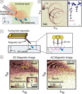
While the spatial resolution of a scanning NV magnetometer is generally determined by proximity to the samples, the resolution can still be improved by applying an additional magnetic field gradient, if the targeted magnetic sample consists of paramagnetic spins that can be spectrally driven.Reference Taylor, Cappellaro, Childress, Jiang, Budker, Hemmer, Yacoby, Walsworth and Lukin 8 Under magnetic field gradients, two otherwise identical paramagnetic spins at distant locations experience different magnetic fields, resulting in spectrally separated spin resonance frequencies. This spectral separation allows for selectively driving spins at particular locations and therefore can be converted to spatial resolution. This method has recently been applied to spatially image optically irresolvable proximal NV centersReference Grinolds, Maletinsky, Hong, Lukin, Walsworth and Yacoby 20 ( Figure 5 a–b). In this demonstration, a magnetic tip with a high field gradient (∼20 μT nm–1) was scanned relative to three identical NV centers while a microwave field of a fixed frequency was continuously applied. As a result, three identical magnetic resonance rings of the three NV centers appeared corresponding to points where magnetic field gradients brought the ESR transition on resonance with the external microwaves. The spatial resolution in this image was 8.9 nm, which could further be improved using higher field gradients.
(a) Magnetic field gradient for improved spatial resolution. Identical paramagnetic spins (here, identical nitrogen-vacancy [NV] spins at the same NV orientation) at distant locations experience different magnetic fields and are thus spectrally separated in the frequency domain. The spectral linewidth of the spins is converted to the spatial resolution by magnetic field gradients. Adapted with permission from Reference Reference Grinolds, Maletinsky, Hong, Lukin, Walsworth and Yacoby20. © 2011 Nature Publishing Group. (b) Magnetic resonance image of three identical NV spins. Three identical rings with widths of 8.9 nm manifest an improvement of roughly two orders of magnitude in spatial resolution compared to standard diffraction-limited optical images. Adapted with permission from Reference Reference Grinolds, Maletinsky, Hong, Lukin, Walsworth and Yacoby20. © 2011 Nature Publishing Group. (c) Motion-enabled AC magnetometry with a single NV center. In this measurement, periodic relative motion between the sample (magnetized tip) and the sensor (NV spin) was induced by a tuning fork resonator (right), allowing the application of an optimally sensitive AC imaging scheme to a static and spatially varying magnetic sample (here, the magnetized tip). Adapted with permission from Reference Reference Hong, Grinolds, Maletinsky, Walsworth, Lukin and Yacoby21. © 2012 American Chemical Society. (d) Magnetic images of the tip acquired by the DC sensing scheme (left) and motion-enabled AC sensing scheme (right). In the motion-enabled AC magnetic image, additional features of multiple fringes were observed, indicating higher magnetic field sensitivity. Adapted with permission from Reference Reference Hong, Grinolds, Maletinsky, Walsworth, Lukin and Yacoby21. © 2012 American Chemical Society.

While an “AC sensing magnetometry scheme” is desired for achieving higher magnetic field sensitivity, it requires AC modulation of the magnetic field from sensing targets. However, such modulation is difficult to achieve in samples with static magnetizations such as ferromagnetic or anti-ferromagnetic orders. This problem can be circumvented by exploiting the periodic oscillation of the AFM tip, which holds the scanning NV magnetometer (Figure 5c). This periodic motion of the NV center relative to a sample transforms the spatially varying magnetic field of the sample to a time varying magnetic field, allowing for employment of AC detection schemes. This motion-enabled AC magnetometry has recently been demonstrated in imaging a magnetic tip.Reference Hong, Grinolds, Maletinsky, Walsworth, Lukin and Yacoby 21 In contrast to DC magnetic imaging (Figure 5d), it reveals additional spatial features, which is the result of the improved magnetic field sensitivity of AC sensing.
This recent progress in scanning NV magnetometry could open up a new regime in probing nanoscale magnetic phenomena. The demonstrated combination of AC magnetic field sensitivity (56 nT Hz–1/2) and close proximity to the sample (∼25 nm) would potentially allow for imaging single electron spins on the surface within a second of integration time at room temperature, as the magnetic field from a single electron spin at a distance of 25 nm is roughly 60 nT. Furthermore, the presented method of applying field gradients could potentially allow subnanometric spatial resolution, and the motion-enabled AC sensing scheme would provide a versatile magnetometry platform, not restricted to specific kinds of samples.
Magnetometry with large ensembles of NV centers
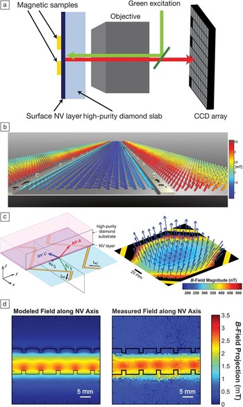
Another promising approach to NV-based magnetic field imaging extends measurements to ensembles of NV centers, thus improving the magnetic field sensitivity by a factor of 1/√N, where N is the number of NV centers within the optical detection volume.Reference Taylor, Cappellaro, Childress, Jiang, Budker, Hemmer, Yacoby, Walsworth and Lukin 8 Preliminary demonstrations of magnetic field imaging using ensembles of NV centers have measured magnetic fields at the surface of a diamond chip.Reference Maertz, Wijnheijmer, Fuchs, Nowakowski and Awschalom 22 – Reference Pham, Sage, Stanwix, Yeung, Glenn, Trifonov, Cappellaro, Hemmer, Lukin, Park, Yacoby and Walsworth 24 In the first demonstration, a confocal microscope was used to restrict the measurement volume to ∼1 μmReference Mansfield 3 near the surface of a diamond (containing a uniform density of NV centers) and sequentially scan the measurement volume over a two-dimensional grid.Reference Maertz, Wijnheijmer, Fuchs, Nowakowski and Awschalom 22 A key advantage of NV-ensemble-based magnetic field sensing, however, is that it is compatible with rapid, wide field-of-view magnetic imaging; in other demonstrations, the signals from NV centers distributed across the surface of a diamond were simultaneously imaged onto a charge-coupled device (CCD), where each pixel corresponded to a position on the diamond.Reference Steinert, Dolde, Neumann, Aird, Naydenov, Balasubramanian, Jelezko and Wrachtrup 23 , Reference Pham, Sage, Stanwix, Yeung, Glenn, Trifonov, Cappellaro, Hemmer, Lukin, Park, Yacoby and Walsworth 24 Wide-field microscopes have a relatively large depth of field, so in this modality, the NV centers must be confined to a thin layer near the diamond surface, either by implanting nitrogen ions in a pure diamond substrateReference Steinert, Dolde, Neumann, Aird, Naydenov, Balasubramanian, Jelezko and Wrachtrup 23 , Reference Pham, Sage, Stanwix, Yeung, Glenn, Trifonov, Cappellaro, Hemmer, Lukin, Park, Yacoby and Walsworth 24 or by incorporating a thin layer of nitrogen-rich diamond during diamond synthesis.Reference Pham, Sage, Stanwix, Yeung, Glenn, Trifonov, Cappellaro, Hemmer, Lukin, Park, Yacoby and Walsworth 24
The projections of the magnetic field were measured along each of the four distinct N–V symmetry axes present in the ensemble population and combined to form images of the three-dimensional (3D) vector magnetic field pattern in the NV plane. This 3D vector magnetometry capability offers a potential advantage over single NV measurements, which are only sensitive to the magnetic field projection along a single N–V symmetry axis. Figure 6 shows measured vector magnetic fields from current carrying metal wiresReference Steinert, Dolde, Neumann, Aird, Naydenov, Balasubramanian, Jelezko and Wrachtrup 23 , Reference Pham, Sage, Stanwix, Yeung, Glenn, Trifonov, Cappellaro, Hemmer, Lukin, Park, Yacoby and Walsworth 24 patterned onto the diamond surface. The image in Figure 6b was acquired by sweeping the applied microwave frequency and locating the ESR peak pairs corresponding to the four NV crystallographic axes, while Figure 6c was imaged using the AC sensing scheme with a 210 μs phase integration time (4.75 kHz).Reference Pham, Sage, Stanwix, Yeung, Glenn, Trifonov, Cappellaro, Hemmer, Lukin, Park, Yacoby and Walsworth 24 In the study by Steinert et al.,Reference Steinert, Dolde, Neumann, Aird, Naydenov, Balasubramanian, Jelezko and Wrachtrup 23 the ∼60 μm × 60 μm field of view was divided into 100 nm pixels containing ∼10 NV centers each, and the diffraction-limited optical resolution was 250 nm. A typical ESR frequency sweep was acquired in 75 s and resulted in σ ∼10 μT uncertainty in the measured field projection along each NV axis in each pixel.Reference Steinert, Dolde, Neumann, Aird, Naydenov, Balasubramanian, Jelezko and Wrachtrup 23 In the study by Pham et al.,Reference Pham, Sage, Stanwix, Yeung, Glenn, Trifonov, Cappellaro, Hemmer, Lukin, Park, Yacoby and Walsworth 24 the 140 μm × 140 μm field of view was divided into 614 nm pixels containing ∼100 NV centers each, and the diffraction limited resolution was ∼500 nm. The AC magnetic field sensitivity measured along each NV crystallographic axis was 136 nT Hz–1/2 in each pixel.Reference Pham, Sage, Stanwix, Yeung, Glenn, Trifonov, Cappellaro, Hemmer, Lukin, Park, Yacoby and Walsworth 24 Pham et al. also demonstrated the ability of the CCD-based NV-ensemble magnetic imager to resolve field patterns, which vary on the micrometer length-scale by measuring the magnetic field produced by AC current flowing through a notched wire pattern at the diamond surface (see Figure 6d).
(a) Schematic of ensemble nitrogen-vacancy (NV) magnetometry. High density layers of NV centers are prepared at the surface of bulk diamond, where magnetic samples are positioned. Spatial imaging of magnetic samples can be acquired by either a standard confocal scanReference Maertz, Wijnheijmer, Fuchs, Nowakowski and Awschalom 22 or a wide-field image with charge-coupled device (CCD) array,Reference Steinert, Dolde, Neumann, Aird, Naydenov, Balasubramanian, Jelezko and Wrachtrup 23 , Reference Pham, Sage, Stanwix, Yeung, Glenn, Trifonov, Cappellaro, Hemmer, Lukin, Park, Yacoby and Walsworth 24 as shown. (b) Vector image of magnetic fields from a pair of parallel metal lines on the diamond surface using CCD.Reference Steinert, Dolde, Neumann, Aird, Naydenov, Balasubramanian, Jelezko and Wrachtrup 23 Adapted with permission from Reference Reference Steinert, Dolde, Neumann, Aird, Naydenov, Balasubramanian, Jelezko and Wrachtrup23. © 2010 American Institute of Physics. (c) Demonstration of vector AC magnetic imaging. Oscillating magnetic fields induced by AC currents carried in zigzag metal strip lines were imaged by an ensemble of NV centers with an improved AC magnetic field sensitivity of 136 nT Hz–1/2 at 4.75 kHz and acquired by CCD. Adapted with permission from Reference Reference Pham, Sage, Stanwix, Yeung, Glenn, Trifonov, Cappellaro, Hemmer, Lukin, Park, Yacoby and Walsworth24. © 2011 IOP Publishing. (d) Modeled (left) and measured (right) image of the magnetic field projection along the N–V axis produced by an AC current through the notched wire pattern (separation ∼1 μm). The frequency and the amplitude of the current were 109.5 kHz and 50 μA, respectively. Adapted with permission from Reference Reference Pham, Sage, Stanwix, Yeung, Glenn, Trifonov, Cappellaro, Hemmer, Lukin, Park, Yacoby and Walsworth24. © 2011 IOP Publishing.

There are a number of avenues for improving upon the first generation of NV-ensemble-based magnetic field imagers. First, better AC magnetic field sensitivity can be achieved by employing more advanced decoupling techniques, such as the XY family of pulse sequences used in NMR.Reference Gullion, Baker and Conradi 25 A factor of 10 improvement in AC magnetic field sensitivity was recently reported, yielding 6.8 nT Hz–1/2 with ∼103 NV centers concentrated in a volume of 30 μm3 and using a 240-pulse XY sequence.Reference Pham, Bar-Gill, Belthangady, Le Sage, Cappellaro, Lukin, Yacoby and Walsworth 26 Second, magnetic field sensitivity can be enhanced by exploiting recently developed efficient fluorescence measurement techniques, such as the side collection schemeReference Le Sage, Pham, Bar-Gill, Belthangady, Lukin, Yacoby and Walsworth 27 and infrared-absorption method.Reference Acosta, Bauch, Jarmola, Zipp, Ledbetter and Budker 28 By combining these two techniques and with denser NV layers, the sensitivity could potentially reach sub-nT Hz–1/2 levels. Third, increasing the conversion efficiency of nitrogen defects to NV centers is an active area of research.Reference Pezzagna, Naydenov, Jelezko, Wrachtrup and Meijer 29 – Reference Schwartz, Aloni, Ogletree and Schenkel 31 In the short term, increasing the N-to-NV conversion efficiency (at current, typically <1% for CVD-grown diamonds and ∼2.5% for ion-implanted diamonds) will improve the magnetic field sensitivity through the square-root dependence on the number of sensors without increasing the number of N impurities. In the long term, if the NV centers are distributed with a sufficiently short length scale, the quantum entangled states of the ensemble could be exploited, breaking the standard quantum limits.
One particularly promising avenue of applications for NV-ensemble magnetometry lies in the study of biological systems. The high spatial resolution, wide field-of-view, rapid magnetic field imaging capability of the CCD-based NV-ensemble magnetometer may be applied toward, for example, implementing MRI at the submicron length scale, measuring the concentration of free radicals during signaling or immune responses, tracking spin-labeled molecules in biological processes, or imaging the microscopic connectivity of neuronal networks.Reference Pham, Sage, Stanwix, Yeung, Glenn, Trifonov, Cappellaro, Hemmer, Lukin, Park, Yacoby and Walsworth 24
Summary
The key features of magnetic sensing with nitrogen-vacancy (NV) centers can be summarized as follows: they offer great magnetic field sensitivity, can be brought near the sample with nanometric length scales, and are robust against varying operating temperatures and pressures. Taking full advantage of these remarkable properties, nanoscale scanning single-NV magnetometry and wide-field ensemble-NV magnetometry were successfully demonstrated. While nanoscale scanning single-NV magnetometryReference Maletinsky, Hong, Grinolds, Hausmann, Lukin, Walsworth, Loncar and Yacoby 19 has achieved field sensitivity that can detect a single Bohr magneton with a few nanometers resolution, wide-field NV-ensemble magnetometryReference Steinert, Dolde, Neumann, Aird, Naydenov, Balasubramanian, Jelezko and Wrachtrup 23 , Reference Pham, Sage, Stanwix, Yeung, Glenn, Trifonov, Cappellaro, Hemmer, Lukin, Park, Yacoby and Walsworth 24 has potential for spatio-temporal studies of microscopic biological phenomena with boosted sensitivity and parallel imaging capability. Moving forward, many possibilities for improving performances are being actively pursued, including material engineering,Reference Balasubramanian, Neumann, Twitchen, Markham, Kolesov, Mizuochi, Isoya, Achard, Beck, Tissler, Jacques, Hemmer, Jelezko and Wrachtrup 15 , Reference Ohno, Heremans, Bassett, Myers, Toyli, Jayich, Palmstrom and Awschalom 17 , Reference Naydenov, Richter, Beck, Steiner, Neumann, Balasubramanian, Achard, Jelezko, Wrachtrup and Kalish 30 , Reference Schwartz, Aloni, Ogletree and Schenkel 31 advanced pulse sequencesReference de Lange, Ristè, Dobrovitski and Hanson 14 , Reference Pham, Bar-Gill, Belthangady, Le Sage, Cappellaro, Lukin, Yacoby and Walsworth 26 and measurement schemes,Reference Grinolds, Maletinsky, Hong, Lukin, Walsworth and Yacoby 20 , Reference Hong, Grinolds, Maletinsky, Walsworth, Lukin and Yacoby 21 and better photon collection methods,Reference Le Sage, Pham, Bar-Gill, Belthangady, Lukin, Yacoby and Walsworth 27 , Reference Acosta, Bauch, Jarmola, Zipp, Ledbetter and Budker 28 continuing the rapid progress of the past few years.