I. INTRODUCTION
The heat transport through a heterosystem consisting of a thin film deposited on a substrate is drastically reduced compared to the heat transport in bulk systems. The interface between the two materials acts as a barrier for thermal diffusion. This resistance of the interface is described by a thermal boundary conductance σK, which was discovered by Kapitza.Reference Cahill, Ford, Goodson, Mahan, Majumdar, Maris, Merlin and Phillpot1–Reference Stoner and Maris3 This results in a discontinuity of the temperature at the interface:
 $$\dot Q = - {\rm{\sigma }}_{\rm{K}} \Delta T\quad.$$
σK correlates the net heat flow  $\dot Q$ across the interface to the temperature jump ΔT at the interface and is basically determined by the energy transmission probability Γ across the interface.Reference Cahill, Ford, Goodson, Mahan, Majumdar, Maris, Merlin and Phillpot1–Reference Stoner and Maris3 Two well-accepted models for the calculation of the transmission probability are the acoustic mismatch model (AMM) and the diffuse mismatch model (DMM).Reference Cahill, Ford, Goodson, Mahan, Majumdar, Maris, Merlin and Phillpot1–Reference Stoner and Maris3 Both models only consider phonons for the heat transport. If the dominant phonon wave length is larger than the interface roughness, the phonons are treated as elastic waves, which are reflected and refracted at the interface. The transmission probability is given by the ratio of energy of the transmitted wave compared to the incoming wave. Using the acoustic equivalents of the Fresnel equations in optics, the transmission probabilities are calculated.Reference Swartz and Pohl2–Reference Miklowittz4 The DMM must be used if the interface roughness is larger than the dominant phonon wave length. In this case, diffuse elastic scattering at the interface is assumed, and the transmission probability is given by the density of states of the two adjacent media—the film and the substrate.Reference Swartz and Pohl2, Reference Stoner and Maris3
Verification of the above mentioned theories requires a suitable experimental model system. The heat transport across the interface should only be governed by phonons. Such model systems are thin bismuth films on silicon substrates. In these systems, the energy transport by electrons and holes is prevented by the formation of a Schottky barrier at the Bi/Si interface.Reference Hricovini, Le Lay, Kahn, Taleb-Ibrahimi and Bonnet5, Reference Bannani, Bobisch and Möller6 Additionally, optical phonons in Bi with a frequency of 2.12 THzReference Sokolowski-Tinten, Blome, Blums, Cavalleri, Dietrich, Tarasevitch, Uschmann, Förster, Kammler, Horn-von Hoegen and von der Linde7 cannot couple to the optical phonons of Si with a much higher frequency of 10–15 THz.Reference Börnstein8 Due to the low group velocity of optical phonons, the heat transport via optical phonons is neglected.Reference Krenzer, Janzen, Zhou, von der Linde and Horn-von Hoegen9 Therefore, the Bi optical phonons are trapped in the Bi film and can only decay into Bi acoustic phonons. This process takes place within a few picoseconds.Reference Hase, Mizoguchi, Harima, Nakashima and Sakai10 As a result, the energy transport is governed by the transmission of acoustic phonons.
The experimental thermal boundary conductance is determined from the cooling behavior of the heterosystem upon excitation by ultrashort laser pulses.Reference Cahill, Ford, Goodson, Mahan, Majumdar, Maris, Merlin and Phillpot1–Reference Stoner and Maris3 From Eq. (1), the temporal cooling of the film with the temperature T f can be derived as follows:
 $$c_{\rm{f}} d{{\partial T_{\rm{f}} (t)} \over {\partial t}} = - {\rm{\sigma }}_{\rm{K}} (T_{\rm{f}} (t) - T_{\rm{s}} (t))\quad,$$
with the substrate temperature T s, the specific heat c f, and the thickness d of the film.Reference Stoner and Maris3 In this study, the Bi film was excited by a femtosecond laser pulse, leading to an almost immediate and homogenous heating of the film. Because of the orders of magnitude smaller absorption coefficient and higher heat diffusion constant of Si compared to Bi, we assume a constant Si substrate temperature. This is confirmed by numerical simulations.Reference Krenzer, Hanisch, Duvenbeck, Rethfeld and Horn-von Hoegen11 This furthermore results in a constant heat capacity in Si. With this assumption, Eq. (2) can be solved by an exponential function with the decay constant τReference Krenzer, Janzen, Zhou, von der Linde and Horn-von Hoegen9, Reference Krenzer, Hanisch, Duvenbeck, Rethfeld and Horn-von Hoegen11:
 $${\rm{\tau }} = c_{\rm{f}} d/{\rm{\sigma }}_{\rm{K}} \quad.$$
Taking c f from the literatureReference Börnstein8 and the given film thickness d, the thermal boundary conductance can be extracted from the experimental data.
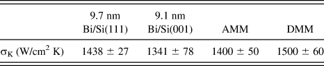
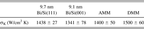
Using the Debye approximation for the density of states, we determine the calculated thermal conductances as σK, AMM = 1400 ± 50 W/(cm2 K) and σK, DMM = 1500 ± 60 W/(cm2 K).Reference Krenzer, Janzen, Zhou, von der Linde and Horn-von Hoegen9 These two theoretical results differ only slightly, which is characteristic for solid–solid interfaces.Reference Swartz and Pohl2
Fundamental studies on the impact of an ordered dislocation array on the thermal heat transport require model systems with and without dislocations that can be reproducibly fabricated. For Bi on Si(001), it has been shown that for films with film thickness above 6 nm, an ordered array of misfit dislocations at the interface is formed.Reference Jnawali, Hattab, Meyer zu Heringdorf, Krenzer and Horn-von Hoegen12, Reference Jnawali, Hattab, Krenzer and Horn-von Hoegen13 In the case of Bi/Si(111), such dislocations are not formed.Reference Kammler and Horn-von Hoegen14, Reference Hirahara, Matsuda, Yamazaki, Miyata, Hasegawa and Nagao15
In spite of the large lattice mismatch between Si and Bi, it is possible to grow high quality epitaxial Bi films with (111) orientation on Si substrates. Bi(111) exhibits a hexagonal surface unit cell with a lattice constant of a Bi(111) = 4.54 Å. With a 6–7 registry, the Bi lattice fits with a remaining compressive strain of only 2% to the Si(111) surface with a lattice constant of a Si(111) = 3.84 Å of its hexagonal unit cell.Reference Jnawali, Hattab, Meyer zu Heringdorf, Krenzer and Horn-von Hoegen12, Reference Jnawali, Hattab, Krenzer and Horn-von Hoegen13 Si(001) has a square unit cell with a surface lattice constant of a Si(001) = 3.84 Å. Along the [ $1\bar 10$] direction, 13 Si lattice constants exactly match 11 Bi lattice constants, i.e., 13 a Si(001) = 11 a Bi(111). Along the perpendicular [
 $11\bar 2$] direction, the remaining compressive strain of 2.3% is relieved to a large extent in a quasiperiodic array of misfit dislocations confined to the interface with a periodicity of a dis= 20 nm. The anisotropic strain of the Bi(111) film with respect to the Si(001) substrate results in the formation of a one-dimensional array of edge dislocations. This array of dislocations results in a periodic undulation of the strain field in the Bi film and in the Si substrate.Reference Jnawali, Hattab, Meyer zu Heringdorf, Krenzer and Horn-von Hoegen12, Reference Jnawali, Hattab, Krenzer and Horn-von Hoegen13, Reference Jnawali, Hattab, Bobisch, Bernhart, Zubkov, Möller and Horn-von Hoegen16
Thus, the impact of an array of misfit dislocations and the impact of different substrate orientations on the heat transport can directly be studied by comparing the experimental results for the thermal boundary conductance of a 9.1-nm-thin Bi film on Si(001) with the thermal boundary conductance of a 9.7-nm-thin Bi film grown on Si(111).
II. EXPERIMENT
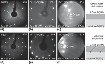
All experiments were performed under ultrahigh vacuum conditions at a base pressure of p base = 2 × 10⁻¹⁰ mbar. The Bi films were prepared in situ in an ultrafast diffraction chamber. Si samples with dimensions of 20 × 3 × 0.5 mm were mounted on a liquid-helium-cooled cryostat, allowing sample cooling down to 20 K. By indirect heating of the sample holder, the sample temperature is varied between 20 and 450 K. Before Bi deposition, the Si samples were degassed for several hours and flash annealed to 1500 K (using direct current heating) to remove the native oxide. Cooling of the Si substrates results in a (7 × 7) reconstructed surface of the Si(111) surface and a c(4 × 2) reconstructed surface of the Si(001) surface, at 90 K. Each sample preparation was checked by low energy electron diffraction (LEED) as shown in Figs. 1(a) and 1(d).
LEED pattern of (a) a (7 × 7) reconstructed Si(111) surface (150 K, 93 eV) and (b) after deposition of a 9.7-nm-thin Bi(111) film (100 K, 79 eV). (c) RHEED pattern of the same film (90 K, 7 keV). (d) LEED pattern of a c(4 × 2) reconstructed Si(001) surface (150 K, 90 eV) and (e) after deposition of a 9.1-nm-thin Bi(111) film (90 K, 91 eV). (f) RHEED pattern of the same Bi film (90 K, 7 keV). The circled areas in (c) and (f) indicate the (00)-spot that was used for the determination of the transient temperature evolution.

Bi with a purity of 99.9999% was deposited from a Knudsen cell-type evaporator.Reference Kury, Hild, Thien, Günter, Meyer zu Heringdorf and Horn-von Hoegen17 The deposited coverage was monitored using a quartz microbalance, which was calibrated ex situ by noncontact atomic force microscopy and x-ray reflectrometry. The Bi(111) films were prepared by deposition of a template film of 6 nm at 150 K. After deposition, the films were annealed to 420 K and afterward held for 10 min at 400 K. Further deposition up to the desired thickness was performed at 400 K. This recipe for film growth under ultra-high vacuum (UHV) conditions results in single crystalline, flat, and well-ordered Bi films.Reference Jnawali, Hattab, Meyer zu Heringdorf, Krenzer and Horn-von Hoegen12, Reference Yaginuma, Nagao, Sadowski, Pucci and Sakurai18 The film morphology was checked before and after each experiment via LEED to ensure reproducibility. Figure 1(b) shows a LEED image of the 9.7-nm-thin Bi(111) film on Si(111). The hexagonal symmetry is typical for the Bi(111) film growth. In Fig. 1(e), the LEED pattern of the 9.1-nm-thin Bi (111) film on Si(001) is shown. The 12-fold symmetry is caused by the superposition of two hexagonal LEED patterns rotated by 90°.Reference Jnawali, Hattab, Meyer zu Heringdorf, Krenzer and Horn-von Hoegen12, Reference Jnawali, Hattab, Krenzer and Horn-von Hoegen13 The elongation of the spots is evidence of a periodic array of edge dislocations pinned at the interface. The Burgers vector b = ½[110] of the 90° edge-type dislocation is oriented in the interface plane and perpendicular to the dislocation line. The strain fields of these dislocations cause a periodic height undulation of the surface, which acts as phase grating for the low energy electrons. As a consequence, all spots are split up into a series of satellites with a separation of Δk = 2π/20 nm. This spot splitting is easily seen in high resolution LEED.Reference Jnawali, Hattab, Meyer zu Heringdorf, Krenzer and Horn-von Hoegen12, Reference Jnawali, Hattab, Krenzer and Horn-von Hoegen13, Reference Jnawali, Hattab, Bobisch, Bernhart, Zubkov, Möller and Horn-von Hoegen16 Due to the limited transfer width of the four-grid optics that was used in this study, we only observe spot elongation.
The transient temperature evolution of the heterosystem upon excitation by short femtosecond laser pulses is determined in a pump–probe experiment through time-resolved electron diffraction. Short electron pulses are diffracted at the sample surface. A series of diffraction patterns at variable delays between the pump and probe pulses are taken to monitor the transient change of the spot intensity. The Debye–Waller effect relates the diffraction spot intensity to the surface temperature of the sample, which is determined by the bulk temperature of the film. After a few picoseconds, a homogenous film temperature has evolved that is equal to the surface temperature.Reference Krenzer, Hanisch, Duvenbeck, Rethfeld and Horn-von Hoegen11 The transient film temperature is thus determined from the intensity evolution of the (00)-spot, using a stationary Debye–Waller measurement for calibration.Reference Krenzer, Janzen, Zhou, von der Linde and Horn-von Hoegen9, Reference Janzen, Krenzer, Zhou, von der Linde and Horn- von Hoegen19
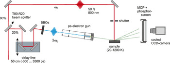
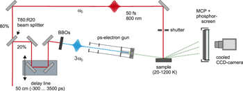
The femtosecond laser pulses are generated by a commercial regenerative amplifier system (Legend, Coherent) with an output power of 2.3 W at a repetition rate of 5 kHz. This system provides laser pulses at a wave length of 800 nm (1.55 eV) with durations of 50 fs. Each laser pulse is split into a pump beam and a probe beam, whose relative optical path lengths are adjusted via a mechanical delay stage. The 80% intensity part of the initial femtosecond laser pulse is used to excite the sample under normal incidence: the pump beam. The laser fluence was 2.3 mJ/cm2 for all experiments. Bi as a semimetal can be efficiently excited by 1.55 eV photons with an absorption length of α−1 = 12.7 nm.Reference Ha and Greene20 The 20% intensity part of the initial laser pulse traverses the mechanical delay line, is frequency tripled, and directed onto a 10-nm-thin Au cathode. Via photoemission, ultrashort electron bunches are generated from the back-illuminated Au cathode. The electron pulses are accelerated to 7 keV and diffracted at the sample. Surface sensitivity is ensured using a grazing incidence angle of ∼5°, which is a typical reflection high energy electron diffraction (RHEED) setup. The diffraction patterns are intensified by a microchannel plate (MCP) and recorded from a phosphor screen with a cooled CCD camera.Reference Janzen, Krenzer, Zhou, von der Linde and Horn- von Hoegen19 The pump–probe setup is shown schematically in Fig. 2. In such a time-resolved experiment, diffraction patterns are recorded at a variety of delay times between −300 and 3500 ps.
Schematic of the experimental pump–probe time resolved reflection high energy electron diffraction (tr-RHEED). The initial 800-nm 50 femtosecond laser pulse is split by a T80:R20 beam splitter into two parts. The more intensive beam is used to excite the sample. The other part of the beam traverses a delay line of variable length, then is frequency tripled, and used to generate the short electron bunches. The diffraction patterns are recorded by a cooled CCD camera from a combination of a 40-mm MCP and a phosphor screen.

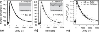
The transient temperature evolution of a 9.7-nm-thin Bi film on Si(111) is shown in Fig. 3(a). This curve is subdivided into three parts. Negative delays represent the sample before the excitation and corresponding to a constant surface temperature of 90 K. The temperature jump at zero delay reflects the response of the system upon excitation by the femtosecond laser pulse. The slope of the temperature rise is determined by the temporal resolution of the experimental setup. The temporal resolution of 40 ps is dominated by the so-called velocity mismatch between the laser pump pulse and the electron probe pulse.Reference Janzen, Krenzer, Zhou, von der Linde and Horn- von Hoegen19 The Bi film is heated by more than 100 K within a few picoseconds. Subsequently, the Bi film cools exponentially with a decay time constant of τ = (803 ± 15) ps for positive delay times. The asymptotic convergence to the base temperature of 90 K for delay times larger than 3 ns is evidence of the negligible heating of the Si substrate.
Transient temperature evolution of (a) a 9.7-nm-thin Bi(111) film on Si(111) and (b) of a 9.1 nm-thin Bi(111) film on Si(001) upon excitation with a 50 femtosecond pulse at a fluence of 2.3 mJ/cm2. The exponential decay time constants are for the 9.7 nm Bi/Si(111) τ = (803 ± 15) ps and the 9.1 nm Bi/Si(00) τ = (807 ± 50) ps. The base temperature T 0 for the experiments was 90 K. In (c), the normalized temperature evolutions are shown.

The result for the Bi film grown on Si(001) with a comparable film thickness of 9.1 nm is shown in Fig. 3(b). A decay time constant τ = (807 ± 50) ps is determined. The normalized cooling behaviors for both systems are the same within the error, as shown in Fig. 3(c).
III. DISCUSSION
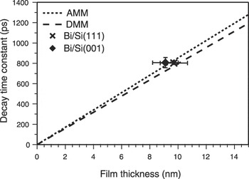
Figure 4 depicts the two decay time constants in comparison to the predictions from AMM and DMM. Previously observed thermal boundary conductances were up to an order of magnitude larger than theoretically predicted.Reference Stoner and Maris3, Reference Stevens, Smith and Norris21 Due to the preparation under UHV conditions, the high quality of the epitaxial grown Bi films with an abrupt interface leads to a much lower thermal boundary conductance. The experimental values for 9.1 and 9.7 nm-thin films agree well with the theoretically determined decay constants, which are proportional to the film thickness.
Thickness dependence of the decay time constant calculated with the AMM and DMM in comparison to the experimental determined decay time constants of a 9.7 nm Bi(111)/Si(111) and a 9.1 nm Bi(111)/Si(001).

Using literature values for the heat capacity c f and applying Eq. (3), a thermal boundary conductance of σK, Bi/Si(111) (140 ± 50 K) = (1438 ± 27) W/(cm2 K) for the 9.7 nm-thin Bi film on Si(111) is extracted.Reference Börnstein8 The error margins originate from the determination of the decay time constant. For the 9.1-nm-thin Bi film grown on Si(001), a thermal boundary conductance of σK, Bi/Si(001) (165 ± 75 K) = (1341 ± 78) W/(cm2 K) is calculated. The error margins for the temperature display the temperature range in which the thermal boundary conductance is valid. The deviation between both experimental thermal boundary conductances is less than 7%. Within the error margins, the values are indistinguishable (see Table I).
Thermal boundary conductances σK for the Bi on Si heterosystem. The theoretical values calculated within the AMM and DMMReference Börnstein8 and the experimentally determined values for a 9.7 nm-thin Bi film on Si(111) and a 9.1 nm-thin Bi film on Si(001) using Eq. (3) with the literature values c f for bulk Bi and the film thickness d.Reference Börnstein8
This result surprises because for Bi films on Si(001), an ordered array of dislocation is formed, which considerably distorts the lattice of the Bi film in the interface region. Each dislocation is surrounded by a strain field.Reference Nabarro22 Such strain fields cause vertical u ⊥(r) and lateral u ‖(r) displacements of the atoms. The distortion of the lattice is largest in the interface plane and in the direct vicinity of the dislocation. Between the dislocation lines, the Bi lattice in the interface plane is in registry with the much stiffer Si lattice [YSi(001) = 130 × 109 Pa and YBi(001) = 32 × 109 Pa]: the Bi is laterally compressed by ε‖ = −2.3%. Due to the large difference in Young’s modulus, the corresponding strain field in the Si substrate is much smaller. The Bi lattice above the edge-type dislocations is expanded by more than ε‖ > 2.3% because one Bi lattice plane is taken out by the dislocation, which causes large tensile stress. As solids tend to conserve their volume upon transverse contraction, the Bi film reacts with a tetragonal distortion, which is described by the Poisson’s ratio ν. The compressed area between the dislocations reacts through an increase of the Bi layer separation by  ${\rm{\varepsilon }}_ \bot = - {\rm{\varepsilon }}_\parallel {\rm{2}}v$. Above the dislocations, the Bi layer separation is reduced by
 ${\rm{\varepsilon }}_ \bot = - {\rm{\varepsilon }}_\parallel 2v$. This lateral undulation of the vertical component u ⊥(r) of the strain field is easily seen in scanning tunneling microscopy and causes spot splitting in high resolution LEED shown in Fig. 1(e).Reference Jnawali, Hattab, Bobisch, Bernhart, Zubkov, Möller and Horn-von Hoegen16, Reference Gradmann and Waller23–Reference Horn-von Hoegen, Schmidt, Meyer, Winau and Riede26 The displacement field u ⊥(r) exhibits a Lorentzian behavior u ⊥(r) = b ‖, edge/π (1 + x 2/z 2)−1 with the edge component b ‖, edge = 3.84 Å of the Burgers vector of the dislocation, x the lateral distance, and z the vertical distance from the core of the dislocation line.Reference Horn-von Hoegen, Al-Falou, Pietsch, Müller and Henzler25, Reference Springholz27, Reference Filimonov, Cherepanov, Paul, Asaoka, Brona and Voigtländer28 The full width at half maxima of this strain field increases with twice the distance to the dislocation line, i.e., the strain fields spread out quickly. The strain fields start to overlap at z = a dis/2. The region with alternating compressive and tensile strain is thus confined to an interface layer with thickness d strain, which is roughly given by half of the dislocation separation a dis, i.e., d strain ≅ a dis/2. With further increasing distance to the interface, the strain fields cancel out each other, and for a thickness d > 2d strain, the Bi film exhibits the relaxed lattice parameter. In the Bi(111)/Si(001) case, we obtain d strain≅ 10 nm, which is of the order of our film thickness.
Despite this locally and strongly varying strained interface layer, we do not observe a significant change of thermal boundary conductance compared to the film without interfacial dislocation network. Interface and strain effects as predicted from molecular dynamics simulations have not been observed.Reference Abramson, Tien and Majumdar29, Reference Li, Maute, Dunn and Yang30 For bulk Si and bulk diamond, a strain reduction of 2.5% leads to enhanced thermal conductivity of 20% and 24%.Reference Filimonov, Cherepanov, Paul, Asaoka, Brona and Voigtländer28 The impact of the dislocations for the thermal heat transport seems to be insignificant under our conditions. The strong influence of the density of dislocations on the thermal boundary conductance has previously been observed in superlattices.Reference Hepplestone and Srivastava31, Reference Lee, Cahill and Venkatasubramanian32 In superlattices, the thermal conductance is decreased along the growth direction. Hepplestone and SrivastaReference Hepplestone and Srivastava31 assume that interface scattering is a result of two effects: the intermixing of atoms at the interface and the presence of dislocations at the interface. The good agreement between their theory and the experimental results from Lee et al.Reference Lee, Cahill and Venkatasubramanian32 supports their model. They conclude that the dominant scattering mechanism at the interface depends on the density of dislocations. In the case of a low dislocation density, scattering is mainly dominated by intermixing of atoms. In contrast, a high density of dislocations dictates the main scattering mechanism itself. Hopkins et al.Reference Hopkins, Duda, Clark, Hains, Rotter, Pinney and Balakrishnan33 have experimentally determined the effect of interfacial dislocations on the thermal boundary conductance across GaSb/GaAs interfaces. They have grown films in interfacial misfit array growth mode (IMF) and non-IMF. The thermal conductance across the interface decreases with increasing misfit dislocation density. The lattice mismatch of 7.8% for the GaSb/GaAs system is more than a factor of 3 larger than in our Bi/Si system, which is only 2.3%. The GaSb film thickness of 500 nm by far exceeds the critical film thickness for the generation of dislocations,Reference Hopkins, Duda, Clark, Hains, Rotter, Pinney and Balakrishnan33 and the films must be relaxed by misfit dislocations. As a result, all films show a high density of dislocations: the IMF films exhibit an interfacial dislocation every 4 nm with a density of threading dislocations of the order of 5 × 10⁶ to 5 × 10⁸ dislocations per cm2, while the non-IMF films exhibit a much higher density of threading dislocations of the order of 109–1011 dislocations per cm2. We prepared a heterosystem—Bi films on Si(001)—which can be compared with IMF GaAs, except that the distance between the dislocations is by a factor of 5 larger as compared to their model system GaAs. The much lower density of dislocations may be the reason that a decrease of the thermal boundary conductance could not be observed. In the Bi/Si(001) system studied here, the density of threading dislocations is below 5 × 10⁸ per cm2.
In our model system, the separation of a dis = 20 nm is much larger than the dominant phonon wave length λd ≅ a 0θD/T, which in our experiments is of the order of the lattice parameter. The short wave length phonons may only be refracted by the slowly varying strain fields. We might expect enhanced scattering or diffraction of phonons only for temperatures when the dominant phonon wave length λd is of the order of a dis, i.e., at temperatures of liquid Helium.
IV. CONCLUSIONS
In this paper, the impact of an interfacial array of dislocations on the thermal boundary conductance was systematically studied for the heteroepitaxial system Bi on Si. Bi(111) films on Si(111) exhibit a compressive strain of 2% without dislocations. For Bi(111) films grown on Si(001), an array of IMF dislocations is formed accommodating the lattice mismatch and relieving the compressive strain. For films with almost identical thicknesses, we determined a thermal boundary conductance for Bi on Si(111) of σK, Bi/Si(111) = (1438 ± 27) W/(cm2 K) and for Bi/Si(001) of σK, Bi/Si(001) = (1341 ± 78) W/(cm2 K). Within the experimental error, these thermal boundary conductances are same for the interfaces with and without dislocations. Additionally, the different substrate orientations Si(001) and Si(111) and therefore the impact of substrate anisotropy seem to play a negligible role. However, we cannot rule out that the dislocation network and anisotropy effects have a noticeable effect on the thermal boundary conductance but cancel out each other.
The experimental values also agree well with predictions for the thermal boundary conductance in the framework of AMM and DMM.
ACKNOWLEDGMENT
Financial support from the Deutsche Forschungsgemeinschaft through SFB 616 “Energy Dissipation at Surfaces” is gratefully acknowledged.