The challenge of on-chip isolation
Isolators, as the photonics counterpart of electrical diodes, play a critical role in photonic integrated circuits (PICs) by preventing harmful feedback between different parts of the circuit. For example, an isolator is often used to protect a laser source from destabilizing feedback or damage from back-reflected light. The need for on-chip isolation becomes imperative as the level of photonic integration continues to scale, since unwanted reflections between the many integrated devices in a PIC are common and can be highly disruptive in a complex optical network.
Fundamentally, optical isolation requires breaking the time-reversal symmetry of light propagation. Such optical nonreciprocity can be realized by using magneto-optical (MO) effects, or nonmagnetic approaches such as indirect interband photonic transitionsReference Yu and Fan1,Reference Lira, Yu, Fan and Lipson2 and nonlinear optics.Reference Shi, Yu and Fan3 Traditional optical isolators used in free-space and fiber-optic systems are almost exclusively based on Faraday rotation in MO crystals, in which a magnetic field is applied along the light propagation direction to induce circular birefringence and polarization rotation. These Faraday rotation isolators typically feature an isolation ratio (the transmittance contrast between forward and backward propagating light) of the order of 30 to 40 dB, an insertion loss (loss of the forward propagating light passing through the isolator) below 1 dB, and an operation bandwidth exceeding 50 nm in the near-infrared (NIR) telecommunication window around 1.5-µm wavelength. Despite the high performance of these free-space isolators, they are bulky discrete devices not suitable for planar on-chip integration. In addition, at present, the price of a discrete isolator ranges anywhere from USD$30 up to more than USD$1,000, a prohibitive cost for large-scale PICs.
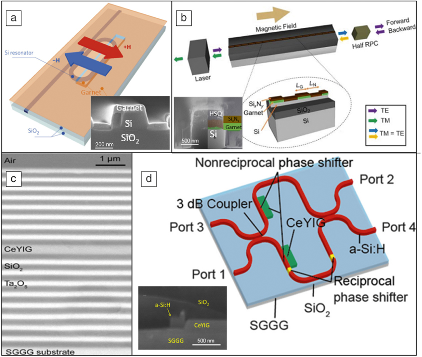
On-chip magneto-optical isolation can be achieved by Faraday rotation,Reference Karki, Stenger, Pollick and Levy4–Reference Zhang, Dulal, Stadler and Hutchings6 nonreciprocal phase shift (NRPS),Reference Dötsch, Bahlmann, Zhuromskyy, Hammer, Wilkens, Gerhardt, Hertel and Popkov7 nonreciprocal loss or gain,Reference Zaets and Ando8 and nonreciprocal mode conversion.Reference Montoya, Parameswaran, Hensley, Allen and Ram9–Reference Hammer, Ozgur, Evans and Butler11 The Faraday rotator configuration used in free-space isolators is sensitive to waveguide birefringence and is not suitable for on-chip optical isolation,Reference Levy5,Reference Dionne, Allen, Haddad, Ross and Lax12 unless a quasi-phase match scheme is implemented (Figure 1b).Reference Zhang, Dulal, Stadler and Hutchings6,Reference Hutchings, Holmes, Zhang, Dulal, Block, Sung, Seaton and Stadler13 Schemes based on nonreciprocal optical loss in an InGaAsP waveguide coated with ironReference Shimizu and Nakano14 and active devices, including an amplifier to compensate for the loss,Reference Van Parys, Van Thourhout, Baets, Dagens, Decobert, Le Gouezigou, Make, Vanheertum and Lagae15 have been demonstrated. Nonreciprocal mode conversion,Reference Shintaku16 cutoff,Reference Tang, Drezdzon and Yoshie10,Reference Hemme, Dötsch and Hertel17 resonant delocalization,Reference El-Ganainy, Kumar and Levy18 and couplingReference Montoya, Parameswaran, Hensley, Allen and Ram9,Reference Hammer, Ozgur, Evans and Butler11 have also been theoretically explored, although experimental realization of on-chip optical isolators and circulators based on these mechanisms has not yet been reported.
(a) Schematic of a nonreciprocal optical resonator structure and scanning electron microscopy (SEM) cross-section image (inset) through the garnet-clad section of the Si waveguide.Reference Bi, Hu, Jiang, Kim, Dionne, Kimerling and Ross38 H denotes the direction in which the magnetic field was applied. (b) Schematic showing a Faraday rotation waveguide isolator and SEM cross section (inset) of the garnet-clad waveguide. Adapted with permission from Reference Zhang, Dulal, Stadler and HutchingsReference 6. © 2017 Nature Publishing Group. Note: HSQ, hydrogen silsesquioxane; RPC, reciprocal polarization converter; L G and L N, length of waveguides with and without magnetic material cladding, respectively. (c) Cross-sectional image of a fabricated one-dimensional magnetophotonic crystal consisting of magneto-optical garnet (CeYIG, cerium-doped yttrium iron garnet) between two SiO2 and Ta2O5 Bragg mirrors on a substituted gadolinium gallium garnet (SGGG) substrate.Reference Yoshimoto, Goto, Isogai, Nakamura, Takagi, Ross and Inoue52 (d) Schematic and SEM cross section (inset) of a Mach–Zehnder transverse electric (TE)-mode isolator with CeYIG mesas adjacent to the side walls of the Si waveguide. Note: a-Si:H, hydrogenated amorphous silicon; TM, transverse magnetic. Adapted with permission from Reference Ishida, Miura, Shoji, Yokoi, Mizumoto, Nishiyama and AraiReference 56. © 2017 The Optical Society.

Unlike Faraday rotation, NRPS is implemented with magnetization perpendicular to the light propagation direction and is insensitive to birefringence.Reference Dötsch, Bahlmann, Zhuromskyy, Hammer, Wilkens, Gerhardt, Hertel and Popkov7 In a typical NRPS device configuration, an applied magnetic field perpendicular to light propagation direction biases the MO material and lifts the degeneracy between forward and backward propagating waveguide modes by inducing a difference in the effective refractive indices of the two modes. The directional dependence of waveguide mode effective index can be leveraged to realize asymmetric light transmission in various device platforms, including Mach–Zehnder interferometers (MZIs),Reference Yokoi, Mizumoto and Shoji19–Reference Shoji and Mizumoto21 microring resonators,Reference Kono, Kakihara, Saitoh and Koshiba22,Reference Zhu and Jiang23 multimode interferometers,Reference Yang, Roh, Ok, Woo, Byun, Lee, Mizumoto and Lee24,Reference Shui, Nie, Zhang, Peng, Xie, Deng and Bi25 and photonic crystals.Reference Kono and Koshiba26 Examples of devices based on a resonator, photonic crystal, and an interferometer are given in Figure 1a, c, and d. These device configurations suffer from limitations such as the large footprint of interferometers and the low bandwidth and high sensitivity to environment of resonators.
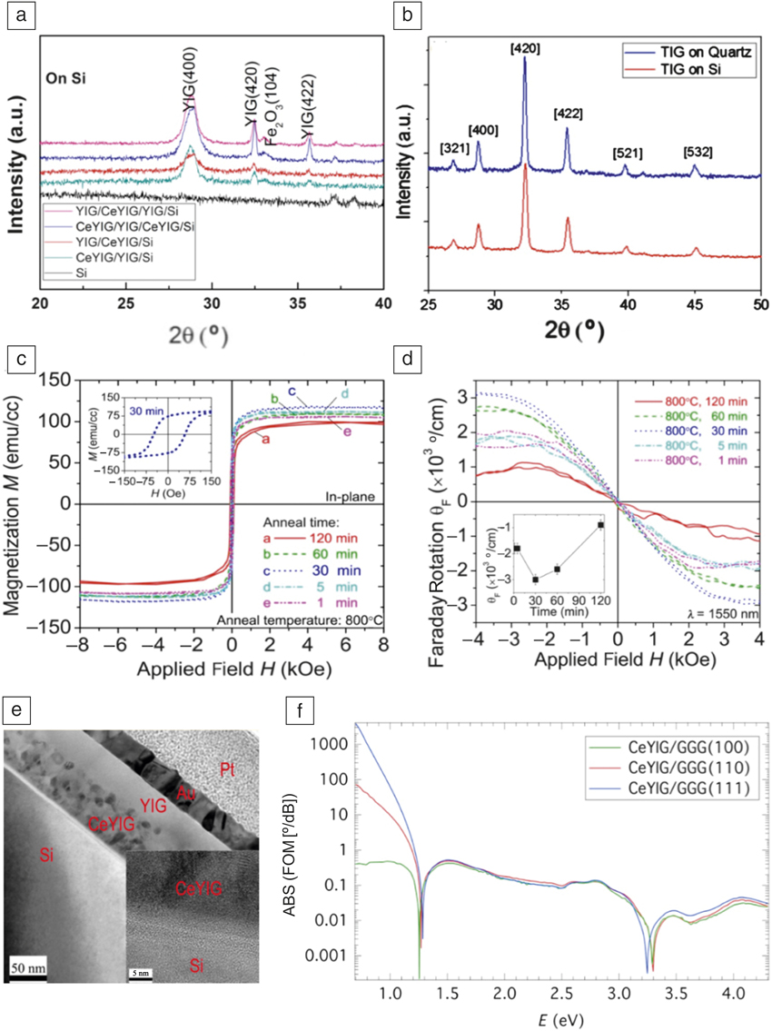
Development of on-chip isolators has been hampered by the incompatibility of traditional MO materials with monolithic integration on semiconductor substrate platforms. Unlike doped-glass-based fiber-optic isolators, the very limited real estate on a chip requires the use of materials with high Verdet constants (i.e., large Faraday rotation) in on-chip isolators. These materials, typically single-crystalline bismuth or cerium-doped yttrium iron garnet (BiYIG, BixY3–xFe5O12 and CeYIG, CexY3–xFe5O12), have attractive figures of merit ([FOM], the ratio of Faraday rotation to optical loss) exceeding 100 degrees/dB in the NIR (Figure 2f), but cannot be monolithically grown on common semiconductor substrates (Si or InP) due to large lattice and thermal expansion mismatch.Reference Boudiar, Payet-Gervy, Blanc-Mignon, Rousseau, Le Berre and Joisten27
(a) X-ray diffraction (ω − 2θ) scans of pulsed laser deposition cerium-doped yttrium iron garnet (CeYIG) and YIG multilayer garnet films after rapid thermal annealing at 800°C for 5 min on silicon, showing characteristic garnet peaks.Reference Sun, Du, Goto, Onbasli, Kim, Aimon, Hu and Ross46 (b) Scans of sputtered terbium iron garnet (TIG) on Si and quartz substrates, showing characteristic garnet peaks. Adapted with permission from Reference Dulal, Block, Gage, Haldren, Sung, Hutchings and StadlerReference 51. © 2016 American Chemical Society. (c) In-plane hysteresis loops and (d) out-of-plane Faraday rotation hysteresis loops at a wavelength (λ) of 1550 nm, with magnetic field and light propagation perpendicular to the film, for sputtered CeYIG on Si substrates annealed at 800°C for various times.Reference Goto, Onbasli, Kim, Singh, Inoue, Kimerling, Ross and Ross43 Inset in (c) is a zoomed-in view at a low magnetic field range, and shows the dependence of saturation Faraday rotation on annealing time. (e) Bright-field transmission electron microscope cross-sectional image of YIG/CeYIG/silica/Si, showing large-grained YIG top seed layer and fine-grained CeYIG.Reference Sun, Du, Goto, Onbasli, Kim, Aimon, Hu and Ross46 (f) Figure of merit (FOM) of single-crystal CeYIG films with different crystal orientations on a gadolinium gallium garnet (GGG) substrate, with magnetic field and light propagation perpendicular to the film.Reference Onbasli, Beran, Zahradník, Kučera, Antoš, Mistrík, Dionne, Veis and Ross44

Two routes have been pursued to resolve the integration challenge—the hybrid approach, which relies on wafer bonding of garnet crystals,Reference Shoji, Mizumoto, Yokoi, Hsieh and Osgood28–Reference Pintus, Huang, Zhang, Shoji, Mizumoto and Bowers33 and the monolithic approach, which directly deposits polycrystalline ferromagnetic oxides or doped semiconductors or polymersReference Zaman, Guo and Ram34–Reference Amata, Royer, Choueikani, Jamon, Parsy, Broquin, Neveu and Rousseau37 on substrates. The former approach can leverage the large Verdet constant and low material absorption in single-crystalline garnets to achieve good isolation performance; however, the wafer-bonding process required by this approach is expensive and limits fabrication throughput and yield.
Deposited polycrystalline ferromagnetic oxides, on the other hand, offer a promising path toward monolithic integration of optical isolators directly on semiconductor substrates with improved fabrication throughput and yield. One limitation with this approach is the inferior optical performance of these polycrystalline thin films, which so far exhibit lower Faraday rotation and higher optical absorption compared to their single-crystalline counterparts. The isolator performance is ultimately bounded by the material characteristics, and more specifically, the material MO FOM in units of degrees of rotation per dB loss. Therefore, improving the FOM of MO films is a critical research objective. In addition to enhancing material quality, further reducing the film growth and heat-treatment temperatures to ensure compatibility of the material deposition process with standard complementary metal oxide semiconductor (CMOS) back-end fabrication constitutes another important research thrust.
In this article, we review the progress to date in the growth and characterization of deposited MO garnet thin-film materials for NIR photonics applications. We specifically focus our attention on materials prepared using pulsed laser deposition (PLD) and magnetron sputtering, the two most commonly adopted deposition techniques for MO oxides. Integration of these materials into a planar device platform will be discussed, and the prospects toward efficient on-chip optical isolation will be evaluated in the context of material FOM and processing compatibility.
Monolithic MO thin films: Growth and characterization
The growth of high FOM garnets such as BiYIG and CeYIG requires processes that promote growth of the garnet phase over competing phases such as CeO2 or Bi2O3, particularly on nongarnet substrates where there is no epitaxial stabilization of a garnet phase. Iron garnet phases have been grown directly on substrates such as silica, and use of seed layers of YIG combined with rapid thermal annealing (RTA) has been shown to promote the growth of MO garnets. Figure 2 shows examples of structural characterization, magnetic hysteresis, Faraday rotation, and FOM of MO garnet films on various substrates.
Garnet films have been used in demonstrations of integrated nonreciprocal photonic devices such as isolators and modulators.Reference Bi, Hu, Jiang, Kim, Dionne, Kimerling and Ross38–Reference Sun, Du, Goto, Onbasli, Kim, Aimon, Hu and Ross46 Bi et al.Reference Bi, Hu, Jiang, Kim, Dionne, Kimerling and Ross38 demonstrated the first monolithically integrated optical isolator on a silicon-on-insulator (SOI) platform (Figure 1a) in which the MO garnet was deposited by PLD on a single-mode silicon “racetrack” resonator through a window in the SiO2 cladding layer. A 20-nm-thick YIG seed layer was deposited and crystallized by RTA, and then 80-nm CeYIG (composition Ce1Y2Fe5O12) was grown. The YIG layer stabilizes the CeYIG, and the use of RTA to crystallize the YIG seed layer significantly reduces the overall thermal budget for the garnet film stack. This is beneficial to reduce cracking in the garnet films and to prevent degradation of other parts of the photonic circuit.Reference Sung, Qi and Stadler47,Reference Sung, Qi and Stadler48 Films grown using this method exhibited high MO activity with Faraday rotation up to ∼3000 degrees/cm at 1550-nm wavelength (Figure 2d), compared to single-crystal values of 3300 degrees/cmReference Hu, Sun, Du, Onbasli and Ross45 to 5500 degrees/cm,Reference Onbasli, Beran, Zahradník, Kučera, Antoš, Mistrík, Dionne, Veis and Ross44 and bulk-like saturation magnetization (Figure 2c).
Seed layers have also been applied in forming sputtered polycrystalline CeYIG films.Reference Stadler and Mizumoto32,Reference Hansen and Krumme49 The seed-layer process can be applied to various substrates, including silica and quartz, although oxidation of a silicon nitride-coated substrate was observed during PLD garnet growth.Reference Onbasli, Goto, Sun, Huynh and Ross50 Sun et al.Reference Sun, Du, Goto, Onbasli, Kim, Aimon, Hu and Ross46 introduced a simplified PLD process, by placing the YIG seed layer on top of the MO garnet, then crystallizing both at the same time by RTA. The film structure resulting from this process is shown in Figure 2e. This process gives direct contact between the MO garnet and the waveguide, which maximizes the coupling of light from the waveguide to the MO cladding. This avoids the reduction in net Faraday rotation caused by the opposite sign of FR in YIG versus BiYIG and CeYIG.
Rare-earth garnets have also been developed for MO applications. Dulal et al.Reference Dulal, Block, Gage, Haldren, Sung, Hutchings and Stadler51 sputter-deposited Bi-doped terbium iron garnet (BiTIG), which has the same sign of Faraday rotation as CeYIG and BiYIG, and with opposite sign of Faraday rotation as TIG. The TIG and BiTIG can be grown directly on Si and quartz without a seed layer (Figure 2b), and the magnitude of Faraday rotation was up to 500 degrees/cm at 1550 nm.
Garnet films have also been incorporated into multilayer photonic structures to form magnetophotonic crystals (MPCs). For example, Yoshimoto et al.Reference Yoshimoto, Goto, Isogai, Nakamura, Takagi, Ross and Inoue52 demonstrated a MPC structure consisting of a sputtered 423-nm-thick CeYIG polycrystalline film integrated between two Bragg mirrors of alternating layers of Ta2O5/SiO2 (Figure 1c). The resulting Faraday rotation of the MPC was 30× higher (–2.92 degrees at 1570-nm wavelength) compared to a CeYIG film without the Bragg mirrors.
Device integration toward on-chip optical isolation
Compatibility with PIC processing
A state-of-the-art silicon photonics manufacturing process generally consists of front-end-of-the-line processes, where the active and passive components are formed on a SOI layer, and back-end-of-the-line (BEOL) integration, where the individual components are interconnected via metallization.Reference Lim, Song, Fang, Li, Tu, Duan, Chen, Tern and Liow53 The fact that MO oxide deposition does not require epitaxy and can take place on both Si and dielectrics suggests that BEOL will likely be an ideal insertion point for MO thin-film integration. For instance, the MO oxides can be deposited through windows opened in the dielectric layers. Such BEOL integration of MO materials also minimizes changes to existing photonic manufacturing processes. In this regard, sputtering is likely a preferred deposition method over PLD, given its ability to form uniform thin films over large substrate areas.
A standing challenge for the BEOL integration of MO materials is the high temperature growth and annealing steps involved to ensure good crystalline quality of the films. As discussed in the previous section, significant progress has been made to reduce the thermal budget of MO thin-film processing with a growth temperature of 650°C followed by a short 5-min annealing step.Reference Sun, Du, Goto, Onbasli, Kim, Aimon, Hu and Ross46 While this still exceeds the typical thermal budget of BEOL processing (<500°C), we anticipate that further improvements can be made by adopting garnet compositions with lower crystallization temperatures, or by using processes such as laser annealing.
Correlating material FOM with device performance
For both Faraday rotators and NRPS-based isolators, performance is ultimately dictated by the FOM of the MO material. In Faraday rotators, the polarization plane of light has to be rotated by 45 degrees per pass, hence the insertion loss (IL) is given by:
 $$IL = 45/FOM \left( {{\rm{in\ dB}}} \right)$$.
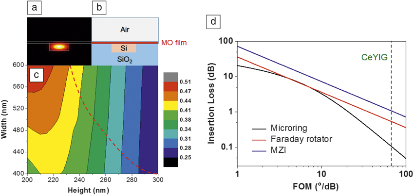
For NRPS-based isolators, the waveguide design affects the NRPS (measured by phase delay per unit waveguide length in degrees/cm) and device performance as well.Reference Sun, Du, Goto, Onbasli, Kim, Aimon, Hu and Ross46 Figure 3c plots the ratio of waveguide NRPS and the MO material’s Faraday rotation (both with the unit of degrees/cm) in an SOI waveguide capped with an MO thin film whose mode profile and cross-sectional configuration are illustrated in Figure 3a–b, respectively. Note that for all waveguide dimensions, the waveguide NRPS is less than the material’s Faraday rotation.
(a) Quasi-transverse magnetic (TM)-mode profile and (b) cross-sectional structure of a magneto-optical (MO) film capped silicon-on-insulator (SOI) waveguide; (c) variation in the ratio of a waveguide nonreciprocal phase shift and the Faraday rotation of the MO material across the SOI waveguide cross-section illustrated in (b); the dashed line delineates the waveguide single-mode (left) and multi-mode (right) regimes. (d) Simulated insertion losses of isolators versus the MO material figure of merit (FOM). Three different device configurations: microring, Faraday rotator, and Mach–Zehnder interferometers (MZIs) are compared. Here, the microring and MZI isolators consist of SOI waveguides shown in (b) with a core width of 450 nm and a height of 220 nm. The dashed line corresponds to the best experimentally assessed FOM in monolithically integrated cerium-doped yttrium iron garnet (CeYIG) films.

Figure 3d presents the computed ILs of three types of isolator devices (Faraday rotators, MZIs, and microrings, where the latter two are both based on NRPS) versus the material FOM. Here the devices considered are ideal—for example, the only source of optical loss results from MO material attenuation, and birefringence of the rotator is assumed to vanish. A semistandard SOI waveguide with dimensions of 450 nm (width) × 220 nm (height) is used for the MZI and microring devices. In all cases, the isolation ratio can, in theory, reach infinity (e.g., for a critically coupled microring or for a power-balanced MZI), and therefore, IL is the proper device performance measure. Figure 3d indicates that Faraday rotators offer the best-in-class performance for a given MO material FOM, provided that their sensitivity to birefringence is properly addressed. This is a direct consequence of the less-than-unity ratio between waveguide NRPS and material Faraday rotation shown in Figure 3c.
Figure 3d allows us to project the performances of monolithic isolators based on available deposited MO thin films. Reliable quantification of FOM can be challenging as accurate loss evaluation in low-attenuation (extinction coefficient k < 10–3) MO thin films is only possible using waveguide measurements. Taking the best experimentally assessed loss data of 40 dB/cmReference Bi, Hu, Dionne, Kimerling and Ross54 and Faraday rotation of 2650 degrees/cmReference Goto, Onbasli, Kim, Singh, Inoue, Kimerling, Ross and Ross43 in PLD-deposited CeYIG films, we obtain a material FOM of 66 degrees/dB. The metric corresponds to ILs of 0.11 dB (microring), 0.54 dB (Faraday rotator), and 1.1 dB (MZI). The result highlights the viability of achieving high-performance optical isolation based on monolithically deposited MO thin films.
Polarization diversity
Besides insertion loss and isolation ratio, polarization diversity is another consideration for isolator device design. This is particularly the case for NRPS-based devices, which to date, almost exclusively adopt a waveguide design similar to the one shown in Figure 3b. The deposited MO film on top of the waveguide core breaks the structural symmetry in the out-of-plane direction and induces NRPS for the quasi-transverse magnetic (TM)-polarized modes. On the other hand, the structure’s in-plane symmetry indicates a vanishing NRPS for the quasi-transverse electric (TE)-polarized modes. Most integrated photonic devices, however, operate with quasi-TE polarization. The polarization mismatch can be handled by adding on-chip polarization splitters and converters to transform the TM modes into TE modes.Reference Dai, Bauters and Bowers55 A second solution involves coating MO materials on one waveguide sidewall to lift the in-plane symmetry for TE-mode isolation. The latter scheme was recently implemented (Figure 1d) by forming an amorphous silicon waveguide adjacent to a patterned mesa of MO garnet grown on a garnet substrate.Reference Ishida, Miura, Shoji, Yokoi, Mizumoto, Nishiyama and Arai56 Angled deposition of MO thin films through windows opened in a thick cladding layer offers another possible route for TE-mode isolators.
Unlike NRPS-based devices, Faraday rotators can operate with both light polarizations. Based on quasi-phase-matched Faraday rotation, the first monolithic TE-mode isolator was experimentally recently demonstrated with an isolation ratio of 11 dB and an insertion loss of 4 dB, which can be further improved with optimized designs.Reference Zhang, Dulal, Stadler and Hutchings6
Summary
Integrated isolators present a challenge due to the need for waveguide-compatible designs with high bandwidth, good fabrication tolerance, polarization diversity, and a small footprint, coupled with the requirement for incorporating magneto-optical materials with a high FOM. Progress, both in device designs based on nonreciprocal phase shift or Faraday rotation as well as the growth of substituted iron garnet films on photonic substrates, have enabled demonstrations of monolithically integrated isolators and suggest the feasibility of manufacturing high-performance integrated devices.
Acknowledgment
The authors acknowledge funding support provided by the National Science Foundation under Award No. 1607865.

Qingyang Du is a doctoral candidate at the Massachusetts Institute of Technology. He received his BS degree in materials physics in 2012 from the University of Science and Technology of China. His research interests include on-chip photonic isolators, radiation damage in photonic materials and devices, and nonlinear photonics in chalcogenide glasses. Du can be reached by email at qydu@mit.edu.

Takian Fakhrul is a graduate student in materials science and engineering at the Massachusetts Institute of Technology. She received her MS and BS degrees in materials and metallurgical engineering at Bangladesh University of Engineering and Technology. Her research focuses on magneto-optical garnet thin films for integrated photonics. Fakhrul can be reached by phone at 716-235-4087 or by email at takianf@mit.edu.

Yan Zhang is a graduate student at the University of Electronic Science and Technology of China. She received her BS degree in materials science in 2010 from Southwest University of Science and Technology, China. Her research interests include magneto-optical materials for applications in on-chip isolators, circulators, and spintronics. Zhang can be reached by email at y_zhang@std.uestc.edu.cn.

Juejun Hu is an associate professor in the Department of Materials Science and Engineering at the Massachusetts Institute of Technology (MIT). He received his BS degree from Tsinghua University, China, in 2004, and his PhD degree from MIT in 2009, both in materials science and engineering. Prior to joining MIT, he was an assistant professor at the University of Delaware from 2010 to 2014. His research interests focus on the field of integrated optics and photonics. Hu can be reached by email at hujuejun@mit.edu.

Caroline A. Ross has been a professor in the Department of Materials Science and Engineering at the Massachusetts Institute of Technology since 1997, preceded by six years at Komag, Inc. and two years at Harvard University. She received both her bachelor’s and PhD degrees from the University of Cambridge, UK. She is a Fellow of the American Physical Society, Materials Research Society, UK Institute of Physics, and IEEE. Her research focuses on magnetic, spintronic, and multiferroic materials, magneto-optical films for integrated photonic devices, and self-assembly of block copolymers and oxide nanocomposites for nanoscale lithography and fabrication. Ross can be reached by email at caross@mit.edu.