I. INTRODUCTION
The market for printed and potentially printed electronics is predicted to be $9.4 billion in 2012,1 where 42.5% will be organic electronics—such as organic light-emitting diode (OLED) display modules. Of the total market in 2012, 30% is said to be printed. Initially, photovoltaics, OLED, and e-paper displays will grow rapidly, followed by thin-film transistor circuits, sensors, and batteries. By 2022, the market is expected to be $63.28 billion, with 45% printed and 33% on flexible substrates.
All applications for printed electronics require electric wiring to transport electrons to (or from) the microelectronic device. Inkjet printing of metal precursor inks has been accepted for the fabrication of microelectronics applications, including conducting wiring for circuitry and radio frequency identification (RFID) tags,Reference Subramanian, Frechet, Chang, Huang, Lee, Molesa, Murphy, Redinger and Volkman2 organic thin-film transistors,Reference Woo, Bae, Jeong, Kim and Moon3 and sensor arrays,Reference Liberski, Delaney, Liberska, Perelaer, Schwarz, Schüler, Möller and Schubert4 as it can enable roll-to-roll (R2R) production in the near future.Reference Perelaer, Smith, Mager, Soltman, Volkman, Subramanian, Korvink and Schubert5 Inkjet printing is an attractive alternative patterning method since it is an additive, noncontact, mask-free, and digital deposition technique, which requires less processing steps and less material,Reference Helgesen, Sondergaard and Krebs6 and produces a minimal amount of waste.Reference Singh, Haverinen, Dhagat and Jabbour7
Conductive precursor materials typically consist of metallic nanoparticles (NPs) or metal–organic complexes, also referred to as metal–organic decomposition (MOD) inks.Reference Kamyshny, Steinke and Magdassi8 Even though there have been many successes in the inkjet printing of metal precursor inks as a rapid fabrication tool for plastic electronic applications, the current challenge is to decrease the processing temperature and time to convert the metal precursor into a continuous and conductive feature.Reference Perelaer, Smith, Mager, Soltman, Volkman, Subramanian, Korvink and Schubert5 To produce flexible electronics, where the devices are prepared on flexible polymer substrates, it is crucial that the processing temperature remains below the glass transition temperature (T g) of the substrate. If the processing temperature exceeds the T g of the polymer foil for a sufficient time, the substrate may become permanently deformed.
Typically, the conversion step that is required to render the precursor compounds conductive requires high temperatures (>250 °C) and long time (>30 min), both of which are not easy to scale to R2R production lines. Both parameters clearly need to be reduced, and this has, therefore, been the research for many scientists over the last few years.Reference Perelaer, Smith, Mager, Soltman, Volkman, Subramanian, Korvink and Schubert5
This review is divided into three parts. After an introduction to printed electronics and inkjet printing, the sintering of inkjet-printed metal precursor inks, including inorganic NPs, and the advantages of using these materials are discussed. Various selective postprinting processes to convert the precursor ink into conductive materials are introduced and compared to conventional thermal sintering. The crucial point here is the fast as well as efficient sintering of the materials, while keeping the underlying polymer substrate unaffected. Mechanisms involved in the sintering process will be discussed as well. Finally, the review concludes with a summary and some comments on the future of printed electronics.
II. SINTERING OF METAL NP INKS
Metal-containing inks are preferred for inkjet printing of conductive features, like contacts and interconnects, due to their superior electrical conductivity relative to conductive polymers.Reference Perelaer, Smith, Mager, Soltman, Volkman, Subramanian, Korvink and Schubert5 Two main types of ink can be distinguished: the first type of ink is a MOD ink,Reference Dearden, Smith, Shin, Reis, Derby and O’Brien9 based on a metal salt dissolved in a suitable solvent. The second type of ink is a suspension of NPs and is referred to as a NP ink.Reference Perelaer, Smith, Mager, Soltman, Volkman, Subramanian, Korvink and Schubert5 In this contribution, we will focus on metal NP inks, as these inks usually have a higher metal loading, are more widely available, and have been reported to have a lower contact resistance.Reference Gamerith, Klug, Scheiber, Scherf, Moderegger and List10
NP inks contain metallic NPs with a diameter between 1 and 100 nm. In 1976, it was found by Buffat and BorelReference Buffat and Borel11 that gold NPs with a diameter below 10 nm reveal a significant reduction in the melting temperature: the melting temperature was reduced from 1064 °C to well below 300 °C when the diameter was below 5 nm. The reduced melting temperature has also been observed for other metals by Jesser et al.Reference Allen, Bayles, Gile and Jesser12 The plot of the melting temperature against the reciprocal of the particle radius exhibits near-linear relationships. It is believed that the size dependence of the melting behavior in particles is related to the internal hydrostatic pressure caused by the surface stress and by the large surface curvature of the particles.
Given the reduced melting temperature of NPs, these particles represent ideal candidates for dispersion in a liquid medium and, subsequently, for inkjet printing. However, when two or more particles are in contact, merging of NPs into larger clusters can take place due to the high surface curvature of the individual NPs. This process takes place with small particles within the medium and at room temperature. Therefore, the NPs have to be protected by an organic layer to prevent agglomeration in solution and to obtain a stable colloidal dispersion.Reference Perelaer, de Laat, Hendriks and Schubert13 Steric stabilization of these particles with an organic additive substantially screens the van der Waals attractions and introduces steep steric repulsion between the particles at contact, which avoids agglomeration. In addition, organic binders are often added to the ink to assure not only mechanical integrity and adhesion to the substrate but also to promote the printability of the ink.
After a NP ink has been printed onto a substrate, a postprinting processing step is required to convert the as-printed patterns into conductive features. This process can be divided in two stages: in the first stage, the organic coating is removed from the metal NP at the curing temperature.Reference Perelaer, de Laat, Hendriks and Schubert13 At this stage, the metal particles make direct physical contact and have a relatively low conductance. In the second stage, larger particles will be formed at the expense of smaller particles due to grain growth, sintering, and the Ostwald ripening. Driven by the size difference between particles, the process of Ostwald ripening stalls when a particle diameter of approximately one and a half times their original size is reached, leaving behind a porous structure, and lower conductivity values than the bulk material are obtained.Reference Kang14 The transport of material between particles during the Ostwald ripening is nonconvective and purely of a diffusive nature. Due to the large surface-to-volume ratio of small particles, a reduction of surface energy, i.e., sintering, will take place, followed by a mass flow to increase the neck radii, and larger particles will form.Reference Goeke and Datye15
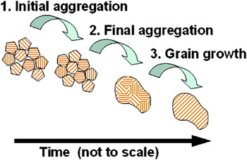
Recently, Ingham et al.Reference Ingham, Lim, Dotzler, Henning, Toney and Tilley16 reported more detailed findings about the mechanism of the Ostwald ripening of surfactant-stabilized gold NPs. The authors followed the processes of aggregation and grain growth in real time by using synchrotron x-ray diffraction and small-angle x-ray scattering techniques. The data showed that initial heating of the nanocrystals causes them to aggregate and to join together as the organic capping agent melts or desorbs. In later stages, hence at higher temperatures and longer times, grain growth was observed. Furthermore, the authors noted that the timescales required for the crystallite sizes to nearly equilibrate are considerably longer than those required for the initial aggregation of the particles. This suggests that when annealing the NPs, there will be a conductivity onset after the initial aggregation (see Fig. 1), and conductivity will continue to increase until grain growth slows down. This suggestion corroborates other findings in literature.Reference Perelaer, de Laat, Hendriks and Schubert13, Reference Volkman, Yin, Bakhishev, Puntambekar, Subramanian and Toney17, Reference Greer and Street18
Schematic diagram showing the mechanisms of coalescence. Reprinted with permission from Ref. Reference Ingham, Lim, Dotzler, Henning, Toney and Tilley16, copyright 2012, the American Chemical Society.

There are three important properties for sintering metal precursor inks: first, a low temperature to convert the ink into its conductive counterpart, which is mainly determined by the amount of organics that are present in the ink.Reference Liang, Shen, Du, Liu, Xie and Gao19 Second, the ink should yield the lowest possible resistivity of the printed features at the lowest possible temperature. To achieve a low resistivity, sintering of the particles is required to transform the initially very small contact areas to thicker necks and, eventually, to a dense layer. High conductivities can then be obtained through the formation of large necks, hence densification, which decreases constriction resistance and eventually forms a metallic crystalline structure with a low number of grain boundaries. Finally, the times required for these processes must be very rapid for R2R applications, where web speeds of several meters per second are typical production speeds.Reference Perelaer, Smith, Mager, Soltman, Volkman, Subramanian, Korvink and Schubert5 Thus, the sintering process should occur preferably within seconds rather than minutes, to keep the production line within practical limits.
A. Conventional thermal sintering
The standard method to convert the as-printed nonconductive inks to conductive patterns involves heating, either on a hot plate or in a convection oven.Reference Greer and Street18 Typically, temperatures above 200 °C are required, and, therefore, substrates with a high thermal stability have been used, such as glass or polyimide.Reference Miettinen, Pekkanen, Kaija, Mansikkamäki, Mäntysalo, Mäntysalo, Niittynen, Pekkanen, Saviauk and Rönkkä20, Reference Scandurra, Indelli, Sparta, Galliano, Ravesi and Pignataro21
Researchers have explored the possibilities to reduce the sintering temperature, e.g., by using low molar mass organic additives. Low sintering temperatures have been reported by Huang et al.Reference Huang, Liao, Molesa, Redinger and Subramanian22 for gold inks. Here, the authors tuned the carbon chain length of alkylthiol capping agents to reduce the decomposition temperature to 130 °C, while obtaining a conductivity of 70% bulk gold. Furthermore, Perelaer et al.Reference Perelaer, de Laat, Hendriks and Schubert13 formulated an aqueous silver ink with less than 5% organic additives, which revealed conductivity already at a temperature of 80 °C.
A serious drawback of using a low content of organic binding materials is, however, that the resulting ink shows short and difficult printability. Organic binders promote the inks printability and are often added to assure mechanical integrity and adhesion to the substrate.Reference Perelaer, de Laat, Hendriks and Schubert13
Recently, Volkman et al. reported that the capping agent is present during the entire sintering process and that its presence significantly influences the grain size and crystallite orientation of the resulting film. Moreover, the film becomes fully conductive in the presence of the capping agent.Reference Volkman, Yin, Bakhishev, Puntambekar, Subramanian and Toney17 It is, therefore, believed that a complete removal of the capping agent is not required to gain conductive features, which is essential for sintering processes taking place at low temperature.Reference Grouchko, Kamyshny, Mihailescu, Anghel and Magdassi23
B. Novel sintering techniques
To reduce production costs and to be able to use substrates with a low thermal stability, i.e., with a low T g, the focus has recently shifted to selective sintering techniques. Therefore, a number of novel alternative sintering methods are listed here.
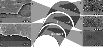
Low-pressure argon plasma is a first example of a selective sintering technique. The method, which was developed by Reinhold et al.,Reference Reinhold, Hendriks, Eckardt, Kranenburg, Perelaer, Baumann and Schubert24 exposes the printed features to a low-pressure argon plasma. This process decomposes, from top to bottom, the organic moieties around the NPs within the printed feature. This process can be followed by a growing skin layer in time, which is depicted in Fig. 2. After a sufficient amount of sintering time, the as-printed features are converted into bulk material. Figure 2 shows, on the left-hand side (I and II), scanning electron microscopy (SEM) images of the transition between two different regions. These regions result from a 2-fold application of the adhesive tape to a sample with repeated plasma sintering. The structural change in the ink is obvious in the lower left picture (II), where sintered and unsintered materials meet. The SEM images on the right-hand side show that the unsintered material looks smooth (V), while obvious grain growth has taken place during sintering (III and IV). The comparison of the microstructures of the samples plasma processed once and twice shows no noticeable difference. Using this technique, an electrical conductivity of 30–40% of bulk silver was obtained.
Skin layer removal and microstructures after repetitive low-pressure plasma sintering. Reprinted with permission from Ref. Reference Reinhold, Hendriks, Eckardt, Kranenburg, Perelaer, Baumann and Schubert24, copyright 2012, the Royal Society of Chemistry.

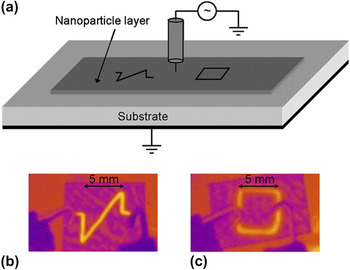
As a second example of selective sintering, rapid electrical sintering (RES) is discussed. Allen et al.Reference Allen, Aronniemi, Mattila, Alastalo, Ojanperä, Suhonen and Seppä25 used a DC current as a selective sintering technique, which requires the features to be slightly conductive prior to sintering. The authors obtained excellent conductivities up to 60% of bulk silver. The features were sintered in very short time of 2 μs, while using a power density of at least 100 nW/μm3. The conductivity of the printed NP layer increases by more than five orders of magnitude during the sintering process. The authors also demonstrated contactless sintering by using a high-voltage probe with an alternating field (100 V, 300 MHz) above a silver NP layer with a ground plate placed beneath, as shown schematically in Fig. 3.
(a) Schematic representation of contactless AC sintering between a probe above the NP layer and a ground plate beneath the printing substrate. IR (λ ∼ 10 μm) images of (b) pulse and (c) square shaped (closed-loop) conductor patterns with U DC = 5 V voltage applied over the conductors for visualization purposes. Reprinted with permission from Ref. Reference Allen, Aronniemi, Mattila, Alastalo, Ojanperä, Suhonen and Seppä25, copyright 2012, Institute of Physics Publishing.

Furthermore, RES of NPs was used to fabricate fully printed low-voltage programmable resistive write-once-read-many (WORM) memory on flexible substrates.Reference Leppäniemi, Aronniemi, Mattila, Alastalo, Allen and Seppä26 The WORM memory devices can be envisioned to be applied, for instance, as low-cost electrically programmable access passes, as event loggers to store sensor information, or as memory elements of RFID tags.
Third, photonic sintering is listed here. In a simplified way, this technique was recently demonstrated using a commercially available camera flash lamp to sinter NPs.Reference Yung, Gu, Lee and Choy27 Photonic sintering uses intense pulsed light with a broad spectrum in the visible range to sinter metal precursor inks in a selective manner, see Fig. 4. The mechanism of photonic sintering is believed to be a thermal conversion of the metal precursor into its conductive counterparts, caused by the high intensity of the flash lamp.Reference Kim, Dhage, Shim and Hahn28 In contrast to conventional thermal sintering, where the sample is exposed continuously to a high temperature, photonic sintering irradiates the sample with multiple short flashes, each with a pulse length in the range of a few micro- to milliseconds. The as-printed dark-colored NP inks have a higher absorbance of the radiant energy of the lamp than the polymer substrate, which results in a faster increase of the temperature in the ink than in the polymer foil. As a consequence, the temperature rises quickly within the ink and causes a rapid sintering of the metal precursor.Reference Ryu, Kim and Hahn29
Also microwave radiation can be used as an alternative and selective sintering technique.Reference Perelaer, de Gans and Schubert30 Typically, highly conductive materials, e.g., metals, have a penetration depth of 1–2 μm at a microwave frequency of 2.45 GHz. It is believed that the conductive particle interaction with microwave radiation, i.e., inductive coupling, is mainly based on the Maxwell–Wagner polarization, which results from the accumulation of charge at the materials interfaces, electric conduction, and eddy currents. In contrast to the relatively strong microwave absorption by the conductive particles, the polarization of dipoles in thermoplastic polymers below T g is limited, which makes the polymer foil’s skin depth almost infinite, hence transparent, to microwave radiation.
R2R photonic sintering tool from NovaCentrix (Austin, TX). Reprinted with permission from PulseForge™ brochure, http://www.novacentrix.com.

Exposing metallic NPs to microwaves does not only reveal a successful sintering process, but also a strong reduction in sintering time, which is hereby decreased by a factor of 20, while conductivity values are similar to those obtained by thermal sintering.Reference Perelaer, de Gans and Schubert30
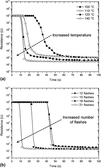
A further reduction of the sintering time was realized by the application of conductive antenna structures around features. Hereby, the exposure times were reduced from 3 min to only a single second. This process is referred to as microwave flash sintering.Reference Perelaer, Klokkenburg, Hendriks and Schubert31 By using visible light photonic presintering, the as-printed features were sintered from their nonconductive status to 28% of the bulk silver conductivity in 10 s without damaging the underlying polymer foil.Reference Perelaer, Abbel, Wünscher, Jani, van Lammeren and Schubert32 When using a thermal pretreatment, a temperature of 140 °C was required to obtain the same results, which was not compatible with the substrates. Figure 5(a) shows the time-dependent resistance of an inkjet-printed line upon thermal presintering at various temperatures, while Fig. 5(b) depicts the same for the photonic presintering example. It can be observed that a significant reduction in resistance as well as sintering time can be achieved by increasing the temperature, for thermal presintering, or increasing the number of flashes, for photonic presintering. However, when using a larger number of flashes, the processing temperature can be kept below the T g of the polymer substrate, while for thermal presintering, increased temperatures are required.
Time-dependent resistance over a single layer line (25 mm length and 500 μm width) upon (a) thermal and (b) photonic presintering (500 W). Reprinted with permission from Ref. Reference Perelaer, Abbel, Wünscher, Jani, van Lammeren and Schubert32, copyright 2012, Wiley-VCH Verlag GmbH & Co.KGaA.

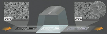
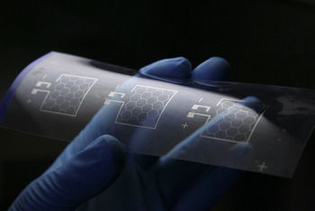
Using both flash sintering techniques, being visible light photonic and microwave sintering, techniques in a tandem wise setup, the as-printed wet silver NPs were sintered in less than 15 s to conductive features with a final conductivity of 40% of the bulk silver value. The combination of inkjet printing and flash sintering enables the production of conductive features at R2R compatible speeds for printed electronics. For example, the obtained conductive honeycomb features can be used for OLED and organic photovoltaics applications, see Fig. 6.
Inkjet-printed honeycomb template sintered using R2R photonic sintering followed by microwave flash sintering. Reprinted with permission from Ref. Reference Perelaer, Abbel, Wünscher, Jani, van Lammeren and Schubert32, copyright 2012, Wiley-VCH Verlag GmbH & Co.KGaA.

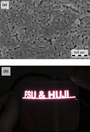
Recently, the combination of plasma presintering and microwave flash sintering was also reported.Reference Perelaer, Jani, Grouchko, Kamyshny, Magdassi and Schubert33 Together with a tailored silver NP ink, conductivity values up to 60% bulk silver were obtained in less than 10 min [Fig. 7(a)]. Typically, these relatively high conductivity values require high sintering temperatures (>450 °C), which are not compatible with polymer substrates.
(a) Top view SEM image of the single layer line after plasma presintering and microwave flash sintering, resulting in a conductivity of 60% of bulk silver; (b) a silver pattern printed on top of a four-layer [PET:indium tin oxide (ITO):ZnS:BaTiO3] EL device. The device illuminates upon applying a voltage between the ITO and the silver electrodes. Reprinted with permission from Ref. Reference Perelaer, Jani, Grouchko, Kamyshny, Magdassi and Schubert33, copyright 2012, Wiley-VCH Verlag GmbH & Co.KGaA.

Electroluminescent (EL) displays were prepared to show the potential application in the field of plastic electronics [Fig. 7(b)], where cost-effective flexible polymer foils, short processing times, as well as high conductivities are preferred for R2R production.
As a fifth technique, LASER radiation has been used to trigger the sintering process locally within the printed features.Reference Ko, Pan, Grigoropoulos, Luscombe, Frechet and Poulikakos34–Reference Kumpulainen, Pekkanen, Valkama, Laakso, Tuokko and Mäntysalo36 Poulikakos et al.Reference Ko, Pan, Grigoropoulos, Luscombe, Frechet and Poulikakos34 used an argon ion LASER beam to sinter printed gold NPs. The beam follows the printed features and converts the central region of the line without affecting the underlying substrate. Using this approach, the authors reported conductivity values up to 25% of bulk gold and a linewidth of 8 μm. One drawback of this approach is the required washing step after sintering to remove the unsintered material. Furthermore, the relatively slow translation speed of 0.2 mm/s, which resulted in the highest conductivity, may limit the usage for R2R applications, although this can be compensated for by using an array of LASER beams in parallel.
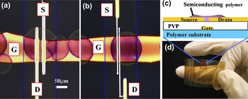
The authors demonstrated the usage of LASER sintering for fabrication of all-inkjet-printed organic field effect transistors (OFETs) (Fig. 8), including a gate, dielectric layer, and semiconductor layer with single digit micrometer resolution, eliminating the need for any lithographic processes. All processing and characterization steps were carried out at plastic compatible low temperatures and in air under ambient pressure.
Micrographs of an OFET test structure with (a) a longer channel (L ∼ 10 μm) and (b) a shorter channel (L ∼ 1.5 μm). “S,” “D,” and “G” indicate source, drain, and gate, respectively. The circles are inkjet-printed semiconducting polymer. The two bright vertical parallel lines are laser sintered gold electrodes (source and drain). The horizontal line is a gate electrode and is under the dielectric layer. The lines indicate the edges of an original inkjet-printed line. (c) Schematics of an OFET. (d) Micrograph of arrays of OFETs fabricated on a polyimide substrate. Reprinted with permission from Reference Ko, Pan, Grigoropoulos, Luscombe, Frechet and Poulikakos34, copyright 2012, Institute of Physics Publishing.

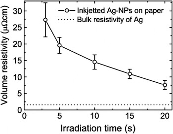
Another promising technique to replace thermal sintering is by using infrared (IR) radiation. Cherrington et al.Reference Worsley, Cherrington, Claypole, Deganello, Mabbett and Watson37 showed that IR radiation can speed up the sintering of silver NPs by a factor 7, while obtaining a similar final sheet resistance. Moreover, by matching the light output of the IR lamp to the absorption spectrum of the ink, a further reduction of the sintering time was reduced to 2 s using near-IR radiation, compared to 600 s for thermal sintering at 140 °C. The slot-die-coated samples revealed a dried film thickness of approximately 3 μm. The authors believe that thinner layers may even improve the sintering times. A more detailed study of IR sintering was performed by Tobjörk et al.,Reference Tobjörk, Aarnio, Pulkkinen, Bollstrom, Maattanen, Ihalainen, Makela, Peltonen, Toivakka, Tenhu and Osterbacka38 where the distance between lamp and sample as well as substrate was investigated. The best performance, hence lowest resistivity of 7.5 μΩ cm, was obtained by irradiating inkjet-printed silver NPs for 20 s at an intensity of 2–4 W/cm2 (see Fig. 9).
Volume resistivity as function of irradiation time for inkjet-printed silver NPs on paper using an IR lamp at an intensity of 2–4 W/cm2. The dashed line indicates the bulk resistivity of silver. Reprinted with permission from Ref. Reference Tobjörk, Aarnio, Pulkkinen, Bollstrom, Maattanen, Ihalainen, Makela, Peltonen, Toivakka, Tenhu and Osterbacka38, copyright 2012, Elsevier Science.

Finally, recent research showed sintering of metallic inks at room temperature, better known as chemical sintering. Coutts et al.Reference Coutts, Cortie, Ford and McDonagh39 showed that thiol-stabilized gold NPs can be sintered at room temperature by using a strong oxidizing gas (NO2). The gas oxidized the protective thiol groups of the ligands, which reduced the ability to bind to the gold surface, and, as a consequence of their small size (4 nm), the particles sintered to form conductive features.
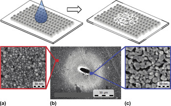
Magdassi et al.Reference Magdassi, Grouchko, Berezin and Kamyshny40 found that silver NPs behave as soft particles when they come into contact with oppositely charged polyelectrolytes and undergo a spontaneous coalescence process at room temperature. Triggered by these findings, the authors have inkjet printed a solution containing the cationic polymer poly(diallyldimethylammoniumchloride) (PDAC) onto an as-printed film of silver NPs that are stabilized by poly(acrylic acid) (PAA) sodium salt, which leads to the sintering of silver NPs and the formation of conductive films without further heating, as depicted in Fig. 10. The obtained conductivity was approximately 20% of bulk silver. The authors believe that the positively charged polymer PDAC removes the charge stabilization that was obtained by the negatively charged PAA stabilizing agent. It was shown that for a PDAC/Ag ratio of 0.12, the zeta potential reached a zero value and precipitation of aggregated NPs occurred. The original NP ink had a zeta potential of −47 mV.
Top: schematic illustration showing what happens when a droplet of PDAC solution is printed onto a silver NPs array. Bottom: SEM image of a printed drop zone (b) and the magnified images of NP arrays after the contact with PDAC outside (a) and inside (c) the droplet zone. Reprinted with permission from Ref. Reference Magdassi, Grouchko, Berezin and Kamyshny40, copyright 2012, the American Chemical Society.

Due to the sintering of NPs at room temperature, the formation of conductive patterns on polymer substrates with a low thermal stability and even on paper is enabled. The authors demonstrated the usability of this process for the fabrication of a transparent polyethylene terephthalate (PET)-based EL device.
Other techniques that are reported in the open literature and have been used for sintering include exposure to ultraviolet radiation,Reference Jahn, Blaudeck, Baumann, Jakob, Ecorchard, Ruffer, Lang and Schmidt41 pulse electric current sintering,Reference Xie, Ohashi, Yamaguchi and Wang42 high temperature plasma sintering,Reference Groza, Risbud and Yamazaki43 and pressure-assisted sintering.Reference Albert, Becker, Keto and Kovar44 However, discussing all alternative sintering techniques is beyond the scope of this overview.
III. CONCLUSIONS AND OUTLOOK
This contribution provided an overview how inkjet printing in combination with metal precursor inks can be used for printed electronics applications. In this particular field, low conversion temperatures of the metal precursors are required, to be compatible with the low thermal stability of the underlying polymer substrate. Typically, substrates with a low glass transition temperature (T g) are used, including PET and polycarbonate, which reduced the maximum processing temperature <150 °C.
The conventional method to convert metal precursor inks into their conductive counterparts is by using heat. Despite high conductivity values that can be obtained using this method, it is not suitable for low temperature sintering, as not only the material to be sintered but also the substrate is exposed to the heat.
A better approach is to direct energy into the metal precursors without affecting the underlying substrate. Several methods that use other energy sources than heat were summarized, including usage of a low-pressure argon plasma, an electrical current, white light photons, microwave radiation, LASER radiation, IR radiation, and a chemical exposure. All techniques are capable of sintering at relatively mild conditions, hence under the T g of the polymer substrate. However, the timescale of the sintering process varies widely. Whereas RES and microwave flash sintering take place at a subsecond timescale, low-pressure argon plasma sintering requires >30 min to complete the sintering process. On the other hand, the upscaling of electrical and microwave sintering are rather difficult, while low-pressure argon plasma sintering can already be performed at a large scale. Therefore, a balance between sample size and sintering speed exists. This, however, can be partly overcome by using a combination of sintering techniques, e.g., using photonic sintering followed by microwave flash sintering.
In recent years, the main focus of research has been to decrease the sintering temperatures and times to obtain the highest conductivity compared to the bulk metal values in a short timeframe. Besides the technical side of sintering, which requires more efficient energy coupling with the material to be sintered, it is also important to tailor the metal precursor inks to improve the conductivity. This approach may be limited due to the existing balance between the ability to print and its ability to sinter; less organic stabilizing materials in the ink increase the ability to sintering but decrease the inks’ printability.
In the near future, an increased concern of using metal-containing inks is the price of raw metals. While the noble metals, gold and silver, are the best electrical conductors, their prices are extremely high compared to other metals. Until now, silver has been the metal that is mostly reported, but other metals are increasingly reported in the open literature, including copper,Reference Jahn, Blaudeck, Baumann, Jakob, Ecorchard, Ruffer, Lang and Schmidt41 nickel,Reference van Hest, Curtis, Miedaner, Pasquarelli, Kaydanova, Hersh and Ginley45 and aluminum.Reference Lee, Choi, Kim, Yun, Jung, Park and Park46 Although these metals may cost only a fraction of gold or silver, their sensitivity toward oxygen makes them hard to handle. Magdassi et al.Reference Grouchko, Kamyshny and Magdassi47 encapsulated copper NP cores in silver shells, which allowed them to use the ink in air. This approach appears to be suitable as no oxides were found to have formed on the inkjet-printed copper patterns after several months. Furthermore, van Hest et al.Reference van Hest, Curtis, Miedaner, Pasquarelli, Kaydanova, Hersh and Ginley45 reported an inkjet printable formulation of a Ni–MOD ink, containing a Ni salt and a low molar mass complexing agent in a reducing solvent. This ink was printed into 80 μm wide lines on a 200 °C glass substrate. Although this temperature is still too high for common polymer foils, the choice of metal is of particular interest since it exhibits a good conductivity, while its price is only a fraction of that of silver.
A rather new approach is to create materials in situ, hence by combining two reactants at the substrate, which will then form the final conductive feature—a technique called reactive inkjet (RIJ) printing.Reference Smith and Morrin48 This is of particular interest when using air-sensitive materials. Calvert et al.Reference Li, Sutton, Burgess, Graham and Calvert49 have reported the preparation of conductive copper lines by using RIJ printing. Conductive copper lines were directly written on paper through inkjet printing of a copper salt and sodium borohydride (NaBH4) as a reducing agent sequentially from two separate compartments of a multicolor HP cartridge. After successive printing, the obtained conductivity was a few percent of bulk copper. Liao et al.Reference Kao, Hung and Liao50 used silver ammonia and formaldehyde solutions from separate printheads; the so-called mirror or Tollens reaction created silver features in situ on the substrate and a final conductivity of 6% of bulk silver.
RIJ allows a printer to be used as a synthesis robot, while also being a versatile patterning technique using the same energy that was used to deposit the reactants. This in particular makes the process more efficient in terms of energy and materials usage. The approach of RIJ printing further reduces the amount of processing steps and is seen as revolutionary,Reference Smith and Morrin48 although it is currently only applicable at the lab scale.
ACKNOWLEDGMENTS
The European Community’s Seventh Framework Programme (FP7/2007-2013) under grant agreement no. 248816 is greatly acknowledged for financial support as well as the Fonds der Chemischen Industrie (FCI) and the Dutch Polymer Institute (DPI, technology area HTE).