I. INTRODUCTION
In the past few decades, finline techniques were widely developed [Reference Knorr and Shayda1–Reference Fernandes4] and used in the microwave and millimeter-wave systems [Reference Meier5]. Finline bandstop filters (BSFs) have some advantages: they are easy to be integrated into the systems; their insertion loss is lower compared with the finline bandpass filters [Reference Meier5, Reference Omar and Schunemann6]. In the case of suppressing narrow band unwanted signals, finline BSFs are better choices than finline bandpass filters. The way to realize finline BSFs is to embed a λg/2 slot resonator in one of the metal fins (λg is the guided wavelength of the finline at the resonant frequency) [Reference Omar and Schunemann6, Reference Vahldieck7]. The finline BSFs using traditional resonator can generate only one transmission zero in the stopband with one resonator and their bandwidth is quite narrow. The extremely narrow bandwidth of the traditional finline BSF limits its engineering applications due to the frequency deviation caused by the manufacturing errors. Although higher-order BSFs with two or more resonators can broaden their bandwidth, their sizes are larger and their insertion loss is much increased [Reference Biswas and Beat8]. Thus, there is a need to broaden the bandwidth of finline BSFs without enlarging their sizes.
Multi-mode resonators are widely used in microwave and millimeter-wave filters to improve their performances in recent years [Reference Bastioli, Marcaccioli and Sorrentino9–Reference Nosrati and Daneshmand11]. Filters designed with multi-mode resonator can realize much wider bandwidth within the same size compared with the filters designed with single-mode resonator [Reference Nosrati and Daneshmand12–Reference Mirzaee, Virdee and Noghanian14]. We can see that multi-mode resonator technology is a perfect way to broaden the bandwidth of finline BSFs. Unfortunately, there is no research reported in terms of finline BSFs with multi-mode resonator. In this work, we proposed a new kind of dual-mode finline resonator. It consists of a λg/2 resonator that generates one resonant frequency and a λg/4 open-stub that generates another resonant frequency. Using the dual-mode finline resonator, a finline BSF, which has two transmission zeros, can be designed easily with only one resonator and its bandwidth is clearly broadened compared with the traditional ones. The effects of frequency offset caused by manufacturing errors are significantly reduced due to the increased bandwidth, meanwhile, the proposed filter inherits the advantages of traditional finline BSFs.
II. THE BANDWIDTH OF TRADITIONAL FINLINE BSFS
Before analyzing our proposed filter, we would like to see the performance of the traditional finline BSF. A series of U-band finline BSFs are designed with different width of the λg/2 resonator shown in Fig. 1. The high frequency structure simulator (HFSS) (a commercial full wave simulation software) simulation results shown in Fig. 2 demonstrate that their relative bandwidth is <0.5%. The width w (shown in Fig. 2) of the resonator can control their bandwidth, but the effect is extremely limited with the maximum bandwidth of 200 MHz under the 20 dB rejection.
The simulation model of finline BSF with a λg/2 slot resonator.

The simulated performance of traditional finline BSFs with different width (w).
The too much narrow bandwidth of the traditional finline BSF limits its engineering applications. Some manufacturing errors may cause frequency deviation while it is unacceptable when the bandwidth is narrow. For example, Fig. 3 shows the frequency deviation caused by the length l (shown in Fig. 3) of the resonator. Each 0.01 mm difference of l may cause 100 MHz frequency deviation and it is unacceptable while its total bandwidth is <200 MHz under 20 dB rejection. And the frequency deviation caused by manufacturing errors may be much more serious at higher frequencies. In such case, there is an urgent need to broaden the bandwidth of finline BSFs.
The frequency deviation caused by the manufacturing errors of l.
III. ANALYSIS OF DUAL-MODE FINLINE RESONATOR
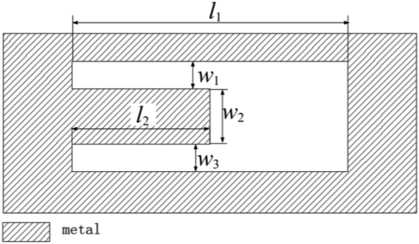
The proposed dual-mode finline resonator is shown in Fig. 4. This resonator can be regarded as a λg/2 slot resonator loading a λg/4 open-stub. When the proposed resonator is embedded in the metal fin instead of the traditional λg/2 slot resonator and excited by an incident quasi-TE10 wave shown in Fig. 1, it can generate two modes: modes A and B shown in Figs 5(a) and 5(b), respectively.
The configuration of the proposed dual-mode resonator.
The electric field layout of the proposed resonator. (a) The electric field pattern of mode A. (b) The electric field pattern of mode B.
The proposed dual-mode resonator is equivalent to one λg/2 shunt resonator and one λg/4 open resonator connected in parallel with a coupling coefficient M AB shown in Fig. 6. The proposed filter, and its equivalent schematics, is shown in Fig. 6. The dual-mode resonator is embedded in one of the metal fins, and this structure can be regarded as the λg/2 shunt resonator and the λg/4 open resonator coupled to the gap of the finline with the coupling coefficient M A and M B, respectively.
The proposed finline BSF and its equivalent schematics.
With the equivalent schematics shown in Fig. 6, it is easy to suppose that the resonant frequency of modes A and B is mainly decided by the dimensions of l 1 and l 2, respectively. Some other dimensions (w 1; w 2; w 3) will mainly affect the coupling coefficient between the two modes and have slight effect on the resonant frequency due to the distribution parameters influence. W c (shown in Fig. 6) will mainly decide the coupling between the main transmission line and the resonator. Smaller W c will increase the coupling between the signal transmission line and the resonator.
The HFSS simulation results fit our analyses well. As shown in Fig. 7(a), f a (the resonant frequency of mode A) varies linearly with the changes of l 1, whereas f b (the resonant frequency of mode B) changes slightly. Meanwhile f b varies linearly with the changes of l 2, while f a changes slightly shown in Fig. 7(b).
Resonant frequency with different values of l 1 and l 2. (a) Resonant frequency of different values of l 1. (b) Resonant frequency of different values of l 2.
Furthermore other sizes of the resonator, such as w 1 (w 2 and w 3) shown in Fig. 4, have little effect on the resonant frequency compared with the length of l 1 and l 2. Fig. 8 shows the changes of the resonant frequency with different value of w 1 (w 2 and w 3) individually, whereas other sizes keep unchanged.
Resonant frequency with different value of w 1 (w 2 and w 3).
As it is shown in Fig. 8, the resonant frequency changes around the center frequency in a narrow range with the changes of w 1 (w 2 or w 3). Meanwhile, when the width of w 1 (or w 2) is wide enough, wider than 0.15 mm, f a keeps relatively unchanged while f b is sensitive to the value of w 1 (or w 2). This is because of the fact that large value of w 1 (or w 2) can weaken the interaction between the two modes and the width of w 1 (or w 2) only affects the equal electrical length of mode B when w 1 (or w 2) is wide enough. f a stays unchanged with different values of w 3, because w 3 only affects the equal electrical length of mode B. This characteristic of the proposed dual-mode resonator can be useful for auxiliary adjustment to achieve the desired target. In this paper, a finline BSF centered at 47.4 GHz with a 20 dB rejection bandwidth of 600 MHz will be designed and fabricated.
IV. REALIZATION OF FINLINE BSF WITH THE PROPOSED DUAL-MODE RESONATOR
With the proposed dual-mode resonator, a finline BSF with two transmission zeros can be conveniently designed with following steps:
1. Decide the center frequency of the finline BSF and calculate the λg [Reference Knorr and Shayda1].
2. Embed the proposed dual-mode resonator in one of the metal fins. Let l 1 = λg/2 and l 2 = λg/4. Other dimensions can be arbitrary within the manufacturing tolerances, but the larger size is better.
3. With the HFSS simulation, adjust l 1 and l 2 to let both of the resonant frequency lay in the desired stopband. Adjust the size of the filter to meet the desired performance.
To confirm the method mentioned in this paper, a finline BSF using the proposed dual-mode resonator was design and fabricated shown in Fig. 9 on the Rogers RT/duroid 5880 with relative permittivity of ε r = 2.2, thickness of h = 0.127 mm, and loss tangent of 0.0009. In order to measure the performance of the finline filter conveniently, this BSF is connected to WR-19 standard rectangular waveguide with finline-to-waveguide transitions using cosine squared lines. The parameters of the designed BSF are l 1 = 2.45 mm, l 2 = 1.03 mm, w 1 = 0.2 mm, w 2 = 0.59 mm, w 3 = 0.2 mm, W c = 0.2 mm, W f = 1.19 mm, L m = 18 mm, L t = 7 mm, g = 0.4 mm, b = 2.388 mm, d = 1 mm, and R = 0.3 mm shown in Fig. 9.
Photograph of the fabricated finline BSF.
V. MEASUREMENT AND RESULTS
The experiment of final fabricated dual-mode BSF is taken under Agilent 8757D Scalar Network Analyzer. The simulated and measured responses of the filter are plotted in Fig. 10. In both responses, it can be clearly observed the two transmission zeros in the stopband. The fabricated BSF presents a 20 dB rejection bandwidth of 600 MHz. The measured insertion loss, including two finline-to-waveguide transitions, is <0.4 dB in the passband (from 40 to 45 GHz and from 50 to 60 GHz). There is a good agreement between the simulated and measured results.
The simulated and measured performances of the designed filter.
VI. CONCLUSION
In this paper, multi-mode resonator technology is applied to finline BSF design. A new type of finline dual-mode resonator was proposed. With this kind of resonator, a finline BSF with two transmission zeros can be easily realized. Compared with conventional finline BSF, the bandwidth of the fabricated filter is clearly extended due to the dual-mode resonator and is three times of the conventional one without enlarging its size. The fabricated BSF presents a 20 dB rejection bandwidth of 600 MHz. The measured insertion is <0.4 dB in the passband. There is a good agreement between the simulated and measured results, therefore it can be mass produced and may have a wide application prospect.
ACKNOWLEDGEMENT
This work was financially supported (partially) by a project (No. IRT1113) under “Program for Changjiang Scholars and Innovation Team in University”.
 Yang Yang was born in Sichuan Province, China, in June 1989. He received the B.S. degree in electromagnetic field and wireless technology from UESTC (University of Electronic Science and Technology of China), Chengdu, Sichuan, China, in 2011, and is currently working toward the M.S. degree in electromagnetic fields and microwave technology at UESTC. His research interests include microwave and millimetre-wave passive components and control circuits design.
 Yong Hong Zhang received the B.S., M.S. and Ph.D. degrees from University of Electronic Science and Technology of China (UESTC), Chengdu, China, in 1992, 1995, and 2001, respectively. He is currently a full Professor in the School of Electronic Engineering, University of Electronic Science and Technology of China. Dr. Zhang is a senior member of the Chinese Institute of Electronics. From 1995 to 2002, he was a lecturer in the University of Electronic Science and Technology of China (UESTC). From2002 to 2004, he was a Postdoctoral Fellow in the Department of Electronic Engineering, Tsinghua University, Beijing, China. His research interests are in the area of microwave and millimetre-wave technology and applications.
 Yong Fan received the B.E. degree from Nanjing University of Science and Technology, Nanjing, Jiangsu, China, in 1985 and the M.S. degree from University of Electronic Science and Technology of China, Chengdu, Sichuan, China, in 1992.
He is now with the School of Electronic Engineering, University of Electronic Science and Technology of China, where he is currently a full Professor. His current research interests include electromagnetic theory, millimetre-wave technology, communication and system. He has authored and co-authored over 130 papers.
 Yu Xiang Li was born in Huaiyuan, Anhui Province, China, in December 1989. He received the B.S. degree in Electromagnetic field and wireless technology from UESTC (University of Electronic Science and Technology of China), Chengdu, Sichuan, China, in 2011, and is currently working toward the M.S degree in electromagnetic fields and microwave technology at UESTC. His research interests include microwave PIN control component design and microwave and millimetre-wave broadband matching technology.