I. INTRODUCTION
Gallium arsenide (GaAs) is a superior semiconductor to silicon for optoelectronic devices due to its ability to handle signals at higher frequencies, at the same time, generate lower noise.Reference Smith, Le, Diadiuk, Hollis, Calawa, Gupta, Frankel, Dykaar, Mourou and Hsiang1, Reference Lam and Macdonald2 However, the application of GaAs is somewhat limited as surface contamination due to oxidation could deleteriously affect the performance of the optoelectronic devices.Reference Saito, Isozaki, Masuda, Fukumoto, Chosa, Ito, Bauer, Inspektor and Oles3 Therefore, surface passivation is critical for improving the reliability of GaAs-based semiconductor devices. Amorphous silicon nitride (SiNx) thin films are one of the most widely used materials for the passivation of GaAs.Reference Yota4 Besides surface passivation, a silicon nitride coating could also act as the dielectric film for metal-insulator-metal (MIM) capacitors in the fabrication of GaAs devices and circuits.Reference Hallakoun, Toledo, Kaplun, Bunin, Leibovitch and Shapira5
For ensuring the reliability of GaAs-based electronic devices, a silicon nitride (SiN) film must adhere well to the substrate to prevent the underlying substrate material from being exposed to atmosphere.Reference Gioti, Logothetidis and Charitidis6 Any damage to the SiN film or debonding of the film from the GaAs substrate could lead to localized oxidation corrosion, which would subsequently cause failure of the passivation. During processing or service, stress being generated at the film/substrate interface may accelerate the detachment of the film from the substrate. Crack and delamination induced at high stress locations would eventually result in the shorting of adjacent structures and electromigration of metals for the SiN/GaAs-based MIM capacitors.Reference Chang, Tsai, Chang, Lin and Chang7 It is therefore important to understand the interfacial failure mechanism of film/substrate structures. With the increasing demand for GaAs-based optoelectronic devices of improved service life, the reliability of bonding between SiN and GaAs has become one of the major concerns for both manufacturers and end users. However, existing studies of SiN/GaAs systems have mainly emphasized the deposition technologies of the passivation layer,Reference Hallakoun, Toledo, Kaplun, Bunin, Leibovitch and Shapira5, Reference Chang, Cibuzar, Vanhove, Nagarajan and Pande8, Reference Jaouad, Aimez and Aktik9 and characterization of the interfacial adhesion has only been explored to a small extent.
Determining the properties of thin film/substrate systems is challenging because for such systems delamination mechanisms depend not only on the mechanical properties of the film, substrate and bonding characteristics at the interface, but also on the stress distribution generated by the applied load during testing. In the last few decades there have been numerable studies dedicated to developing approaches for the understanding of interfacial failure mechanisms, and thus the determination of interfacial strength. A number of testing methods for evaluating the adhesive properties of thin films have been developed, such as indentation,Reference Chang, Tsai, Chang, Lin and Chang7, Reference Yeap, Zeng, Jiang, Shen and Chi10, Reference Singh, Tilbrook, Xie, Bendavid, Martin, Munroe and Hoffman11 scratching,Reference Chang, Tsai, Chang, Lin and Chang7, Reference Bull12, Reference Perry13 stressed overlayer testing,Reference Chen and Bull14, Reference Volinsky, Moody and Gerberich15 pull-out tensile testing,Reference Zhang, Wang, Zeng, Khor, Weng and Sun16 tape peel testingReference Jacobsson17–Reference Kim, Kim and Kim19 and four/three-point bending.Reference Dauskardt, Lane, Ma and Krishna20, Reference Litteken, Dauskardt, Scherban, Xu, Leu, Gracias and Sun21 Uniquely among these techniques, indentation enables investigation of thin-film adhesion in a controllable manner by generating interfacial cracks on a sufficiently small scale and at a specific site. The phenomenon of interfacial fracturing induced by indentation has spurred intense interest, and the indentation approach has thus been accepted as an effective technique for measuring the interfacial toughness of thin coating/substrate materials.Reference DeBoer and Gerberich22–Reference Zhang and Zhang24
In this study, the interfacial adhesion of SiN films on GaAs (001) substrate was investigated using nanoindentation techniques, with a conical indenter. The deformation of the SiN/GaAs bilayer system was first investigated through the study of pop-in and pop-out events that occurred during nanoindentation. Finite element modeling (FEM) simulation was then used to reveal the stress evolution and deformation behavior associated with the indenting process. A model was proposed to interpret the indentation-induced delamination mechanism.
II. EXPERIMENTAL DETAILS
A. Specimens
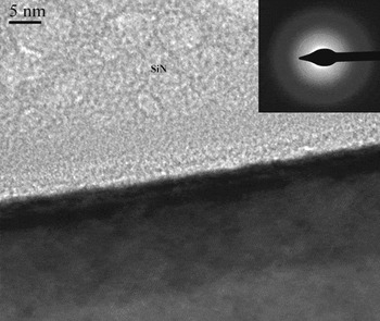
Two SiNx/GaAs bilayer specimens and a GaAs (001) bare wafer used in this study were provided by WIN Semiconductors Co. The SiNx films were deposited using plasma-enhanced chemical vapor deposition (PECVD) on GaAs substrates using a Trikon PECVD system (SPTS Technologies, Newport, Wales). The deposition was performed in a nitrogen atmosphere and a gaseous mixture of SiN4 (at a flow rate of 300 sccm) and ammonia (NH3) (at a flow rate of 600 sccm). The deposition temperature was set at 250 °C. The silicon nitride films coated tend to be nonstoichiometricReference Huang, Winchester, Suvorova, Lawn, Liu, Hu, Dell and Faraone25 (i.e., SiNx with x ≠ 4/3) and have an amorphous structure, as shown in Fig. 1. The films have thicknesses of 490 and 815 nm respectively.
TEM micrograph of PECVD SiN deposited on GaAs substrate. Inserted image is the diffraction pattern of the SiN film, showing typical amorphous structure.

B. Nanoindentation tests
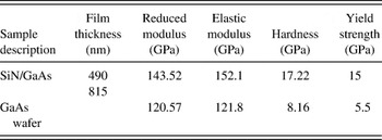
Nanoindentation tests were performed at room temperature on a TI900 Hysitron Triboindenter (Hysitron, Inc., Eden Prairie, MN) that is equipped with an in situ atomic force microscope (AFM). A Berkovich indenter with an included angle of 142.3° and a tip radius of 100 nm was used to measure the elastic modulus and hardness of GaAs substrate and SiN/GaAs bilayer systems. The maximum load was varied from 0.5 to 13 mN. For each load used, at least 10 indents were made on different locations of the specimen. Elastic modulus (E) and hardness (H) of the films were calculated from the load-displacement (P-h) curve using the Oliver-Pharr method for the bare wafer specimenReference Oliver and Pharr26 and the deconvolution method developed by our teamReference Huang, Winchester, Liu, Hu, Musca, Dell and Faraone27, Reference Jung, Lawn, Martyniuk, Huang and Hu28 for the bilayer specimens. The values of E and H are shown in Table I.
Mechanical properties of the specimens.

A conical indenter with a spherical apex was used to study the elastic-plastic deformation mechanics of the film/substrate system, as conical tips create less stress concentration in the film and thus cause less damage to the film structure than the Berkovich tip.Reference Singh, Tilbrook, Xie, Bendavid, Martin, Munroe and Hoffman11 The tip had an included angle of 60° and a tip radius of 10 μm. The indentation load was varied from 10 to 300 mN. For each indentation loading condition, more than five indents were performed at different locations and the average values and standard deviations were computed. After indentation, the indents were examined by the in situ AFM. The AFM showed that the indents were well formed and no significant pile-up occurred.
C. Finite element modeling
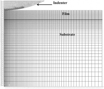
FEM analysis was carried out using the ANSYS program. A 2D axisymmetric FEM model was established to simulate the indenting process. The model region used was 10 times larger than the indented area. The bottom of the substrate was constrained using fixed boundaries. The mesh used had a graduated mesh size, which consisted of 11547 quadrilateral elements, as shown in Fig. 2. Both the substrate and the film were treated as perfectly plastic materials. The elastic moduli used in the model were obtained from the nanoindentation test and the yield strengths were obtained through matching the peak load numerically with the maximum load used in the indentation for a given indentation depth, as shown in Table I. The interface was modeled using a cohesive zone element,Reference Needleman29 where the cohesive energy (i.e., the energy release rate in linear fracture mechanics), Γ, is governed by a constitutive equation known as the traction-separation law30:
 $$\Gamma = e\sigma _{\max } \overline \delta _n \left[ {1 - \left( {1 + \Delta _n } \right)e^{ - \Delta n} e^{ - \Delta t^2 } } \right]\quad,$$
where  $\Delta _n = {\textstyle{{\delta _n } \over {\overline \delta _n }}}$,
 $\Delta _t = {\textstyle{{\delta _t } \over {\overline \delta _t }}}$, σ max is the maximum normal traction at the interface, δ n and δ t are the normal and tangential interfacial separation,
 $\overline \delta _n$ is the normal separation across the interface where the maximum normal traction is attained with δ t = 0, and
 $\overline {\delta _t }$ is the shear separation where the maximum shear traction is attained when
 $\delta _t = {\textstyle{1 \over {\sqrt 2 }}}\overline \delta _t$.
2D axisymmetric finite element model for indentation on bilayer thin film structure contacted by a conical indenter.

The traction T acting on the interface are decomposed into T n and T t in both normal and tangential directions, which can be expressed as
 $$T_n = {{\partial \Gamma \left( \delta \right)} \over {\partial \delta _n }} = e\sigma _{\max } \Delta _n e^{ - \Delta _n } e^{ - \Delta _t ^2 } \quad,$$
 $$T_t = {{\partial \Gamma (\delta )} \over {\partial \delta _t }} = 2e\sigma _{\max } {{\overline \delta _n } \over {\overline \delta _t }}\Delta _t \left( {1 + \Delta _n } \right)e^{ - \Delta _n } e^{ - \Delta _t ^2 } \quad.$$
In the cohesive zone model, traction and strain energy release rates that govern the occurrence of delamination were preset; interfacial failure therefore occurred when the tension at the interface exceeded the preset threshold, assuming that no through-thickness cracking took place. An iterative approach was used to predict the interfacial strength, where the initial cohesive length  $\overline \delta _n$ was set to be 4 nm (which was roughly 1–2% of the film thickness, a value derived during a preliminary simulation). The initial value of σ max was half of the minimum interfacial strength required to prevent delamination.Reference Sheng Liu and Gu31 During modeling, σ max was iteratively adjusted according to the timing of “pop-out” and the slope of the “elbow” from the P-h curve, until the best fit was achieved. Once σ max was found, the cohesive energy could be calculated as
 $$\Gamma = e\sigma _{\max } \overline \delta _n \quad.$$
III. RESULTS
A. Deformation of GaAs (001) substrate
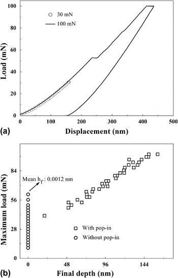
Figure 3(a) shows two typical P-h curves obtained from the indentation processes using two distinctly different loads of 30 and 100 mN. For the load of 30 mN the loading and unloading curves overlap and no residual depth can be observed, indicating that the sample deformed elastically. However, for the load of 100 mN, a distinct pop-in event can be seen on the loading curve. A set of indentations was then carried out at various loads. The maximum loads used for all the indentations are plotted against the final depth h f in Fig. 3(b). For the indentations where pop-in did not occur, the final indentation depths are insignificant, with a negligible mean value of 0.0012 nm indicating that the indentation-induced deformation was nearly elastic. When the load was greater than 60 mN, pop-in always occurred and there existed a linear relationship between the maximum loads used and the final depths of indentation. For loads ranging from 40 to 60 mN, pop-in might or might not occur.
(a) P-h curves of indentations made on the GaAs (001) bare wafer at loads of 30 and 100 mN and (b) the relationship between the maximum load and the final indentation depth.

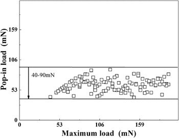
It can also be seen from Fig. 3(a) that the pop-in occurred before the load reached the maximum value. In our tests, pop-in always occurred in the middle of a loading process, except for several indentations with the peak load smaller than 100 mN where pop-in happened during holding. The loads at which the pop-in occurred were plotted as a function of the maximum load used in Fig. 4. The pop-in loads varied from 40 to 90 mN, which appears to be unrelated to the maximum load.
Relationship between the pop-in load and the maximum indentation load for GaAs (001) bare wafer.

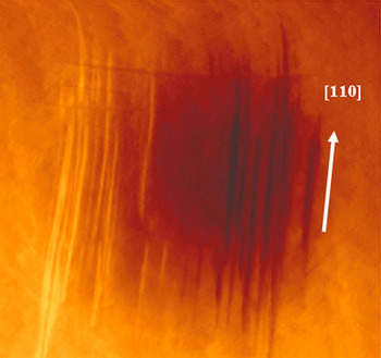
AFM was used to examine the morphology of the indents made. For the indentations in which pop-in did not occur, no observable impression was left on the specimen surface. For those where pop-in occurred, the indent was well formed with insignificant pile-up. However, highly orientated slip bands were observed along the [110] directions, as clearly shown in Fig. 5.
AFM image of the indent made at 100 mN on GaAs (001) bare wafer. (color online)

B. Deformation of SiN/GaAs film/substrate system
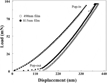
Nanoindentation was also performed on film/substrate systems. Figure 6 shows the typical P-h curves of the two bilayer specimens at the load of 100 mN. Both pop-in and pop-out events could be observed. Similar to the indentation on the GaAs substrate, pop-in occurred during indentation loading. In these cases, the pop-in loads appear to be irrelevant to the maximum load too. For the 490 nm film, the pop-in load varied from 50 to 100 mN, whereas that for the 815 nm film was in the range of 100–150 mN. It is apparent that increased film thickness led to the increased pop-in load.
Typical P-h curves of indentations made at 100 mN on the 490 nm and 815 nm SiN

In contrast to the indentation on the GaAs wafer, a significant pop-out was observed toward the end of the unloading when the bilayer specimens were indented, as indicated in Fig. 6. For those indentations without the occurrence of pop-in, pop-out was never observed. These pop-out events occurring toward the end of indentation unloading are likely due to the interfacial failure of the film/substrate bilayer system, leading to a “elbow” shape curve, or pop-out. To verify this hypothesis, a secondary indentation was conducted at the same location of the first indentation that caused a pop-out.
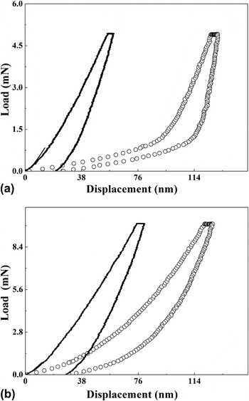
Figure 7 shows the P-h curves obtained from the secondary indentations on the 490 and 815 nm films. In Fig. 7(a), the first indentation was performed at a load of 100 mN, which resulted in a pop-out. The secondary indentation was performed using a load of 5 mN. Here a much smaller load was used in the second indentation to prevent the suspended film being damaged. For comparison, the P-h curve of the (first) indentation performed at 5 mN, but at different location, was also included. It is seen from Fig. 7(a) that in the P-h curve of the secondary indentation a dramatic increase in displacement is observed at approximately 70 nm, both at the beginning of loading and the end of unloading with only a slight increase in load. Similar characteristics were observed when secondary indentation was carried out on the 815 nm film, as shown in Fig. 7(b). Due to the thicker film, a load of 10 mN was applied in the secondary indentation. A displacement jump of about 30 nm was observed, much smaller than that (∼70 nm) in Fig. 7(a).
P-h curves of (a) the secondary indentation at 5 mN made on the spot firstly indented at 100 mN on the 490 nm SiN film; and (b) the secondary indentation at 10 mN made on the spot first indented at 100 mN on the 815 nm SiN film. The curves in solid lines were those obtained from the first indentation using the same loads to the respective secondary indentations.

C. FEM analysis of indentation-induced delamination
The nanoindentation results indicated that the occurrence of pop-in was associated with the noncontinuum deformation feature of GaAs substrate during loading, which will be discussed later. As this study is focused on the indentation-induced interfacial failure, and the corresponding pop-out event that occurred during unloading, the mechanism of the “pop-in” was not modeled with a view to simplify the FEM simulation. In the FEM model, only the unloading section of the P-h curve was used as the optimization target.
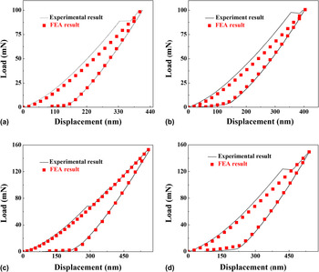
The indentations at different loads were simulated. The traction and the strain energy release rate input into the model for the 490 and 815 nm films were 400 MPa and 1.13 J/m2, respectively. The typical P-h curves of the indentations obtained are shown in Fig. 8. Excellent agreement between the experiment and the simulation was achieved for the unloading section of the curve during which interfacial failure occurred. The loading sections are not perfectly matched, as the FEM model does not account for the effect of pop-in on deformation. However, as this study was focused on the interfacial failure and the associated pop-out that occurred during unloading, the decision to neglect the effects of pop-in had little effect on the result.
Comparison of P-h curves between experiment and the simulation for different loads and film thickness. (a) 100 mN, 490 nm; (b) 100 mN, 815 nm; (c) 150 mN, 490 nm; (d) 150 mN, 815 nm. (color online)

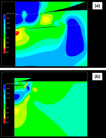
The stress contour underneath the indenter snapped at the moment of delamination for the 490 nm film is shown in Fig. 9(a). It is clearly seen that at debonding a considerable tensile stress of about 400 MPa was built up at the interface toward the center of the indent. The delamination was initiated at the location near the indent center and propagated almost instantaneously in both directions. Figure 9(b) shows the stress distribution when the indenter completely detached from the specimen. At this stage tension was released at the center, but a significant tensile stress was still concentrated at the interfacial crack tip.
Cross-sectional view of the normal stress contours (a) at the initiation moment of interfacial crack and (b) after the indenter completely lost contact with the indented surface. (color online)

IV. DISCUSSION
The occurrence of pop-in during loading was a typical deformation characteristic of GaAs crystal. Pop-in was repeatedly observed in the tests when the indentation load was greater than a critical threshold. Bourhis et al.Reference Le Bourhis and Patriarche32, Reference Le Bourhis and Patriarche33 indented GaAs (001) using a standard Berkovich indenter and found no indentation-induced plastic zone at the indent region using plane-view TEM when the indentation load was below the critical value that triggers the occurrence of pop-in. Taylor believed that pop-in originated with the nucleation of dislocations underneath the indenter using ultralow load and relatively sharp indenters.Reference Taylor, Malshe, Salamo, Prince, Riester and Cho34 When a relatively high load was applied, particularly through the use of spherical indenters, slip bands tended to form at the impression and the dominant cause of the pop-in is likely to be plane slip and twinning.Reference Bradby, Williams, Wong-Leung, Swain and Munroe35, Reference Lloyd, Molina-Aldareguia and Clegg36 In our case, the slip bands along the GaAs [110] directions were observed on the indents in which pop-in occurred, as shown in Fig. 5. Pop-in is therefore attributed to massive dislocation multiplication and motion along favorable directions. This does not preclude the possibility of smaller dislocation movement prior to pop-in, however such small movements are considered unimportant in this study.
A previous study showed that the load that causes pop-in could vary from 0.02 mN to several hundred mN, depending on indenter geometries and loading rates.Reference Taylor, Malshe, Salamo, Prince, Riester and Cho34 In this work, as shown in Fig. 4, the pop-in loads for the bare GaAs substrate varied from 40 to 90 mN. When indenting the bilayers of SiN/GaAs, the load range for pop-in was increased to 50–100 mN for the thinner film and 100–150 mN for the thicker film. An FEM simulation was carried out using the model shown in Fig. 2 to calculate the maximum shear stress inside the GaAs substrate under the pop-in loads. The computed values are 2936–3951 MPa for the bare wafer, 2779–3509 MPa for the thinner film and 3092–3418 MPa for the thicker film. These values are close, indicating that it was the critical shear stress that triggers the occurrence of slip. In summary, when the indentation-induced shear stress in GaAs substrate reached the critical value, pop-in was triggered abruptly in the fashion of plane slip. Prior to this critical stress, the indentation deformation was fully elastic and reversible [see Fig. 3(a)].
The nanoindentation results showed that when indenting the SiN/GaAs bilayers pop-out was always accompanied with pop-in. This suggested that the critical load for generating the pop-out should be greater than that for the pop-in. The indentation-induced delamination at the interface of film and substrate was believed to be responsible for the pop-out. Similar observation was found in the Hainsworth’s and Chen’s study for titanium nitride (TiN)/zirconium nitride (ZrN) multilayer on hard tool steel and TiOxNy on glass substrate, respectively.Reference Hainsworth, McGurk and Page37–Reference Chen and Bull39 The GaAs (001) substrate has lower hardness and elastic modulus, and hence experienced more plastic deformation and less elastic deformation during loading, whilst the SiN film deformed more elastically, bending into the dented GaAs substrate during loading. As a consequence, during unloading more elastic recovery occurred in the SiN film than that in the substrate, resulting in tensile stress developed at the film/substrate interface. Our FEM analysis clearly demonstrated that tension at the interface was built up with the further withdrawal of the indenter during unloading, as shown in Fig. 9. When the tensile stress at the interface exceeded the interfacial adhesion strength, an interfacial crack was initiated and propagated quickly along the interface, causing the film to delaminate from the substrate. The recovery of the delaminated film, in the manner of a centrally deflected plate, results in a sudden load on the tip. As the indentation was a load-controlled process, such a push causes the tip to recede quickly, generating a “pop-out.”
The load-displacement relationship of the secondary indentations at the beginning of loading and near the end of unloading in Fig. 7 clearly suggests that the films, after the first indentation, were locally detached from the substrate and thus behaved like suspended membranes or plates. As shown in Fig. 7, the P-h curves of the secondary indentations suggested that at the starting of loading a smaller load resulted in a significantly greater displacement than the normal deformation of the material, whereas at the very end of unloading a small decrease in load led to a large-scale tip withdrawal. This behaved like loading and unloading on a suspended film. Once the film contacted the substrate, the deformation behavior returned to that of the bilayer system. Certainly, for the same indentation load, lower tensions were generated at the interface for films with greater thickness; a smaller scale of the delamination was therefore induced. This produced a stiffer suspended membrane or plate. Moreover, the delamination induced by nanoindentation has been simulated by FEM using the cohesive zone model. The stress evolution and interfacial crack formation upon unloading agreed well with the delamination mechanism proposed. This is demonstrated in Fig. 8, where the unloading curves of the experimental testing and the FEM simulation are in excellent agreement.
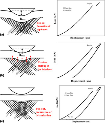
In summary, the indentation-induced deformation process for SiN/GaAs film/substrate bilayer systems can be classified as three stages, as shown schematically in Fig. 10. During loading both the film and substrate were deformed and slip bands were initiated when the stress on the substrate reached a threshold, generating a pop-in, as shown on the loading curve in Fig. 10(a). During unloading both the film and the substrate recover elastically [Fig. 10(b)], and during this phase tension was built up at the interface owing to the mismatch in elasticity, and the difference in existing plastic deformation, between the film and the substrate. When the tensile stress exceeded the interfacial strength delamination occurred, and the detached film recovered elastically upward during unloading. This sped up the tip withdrawal, resulting in a “pop-out” on the unloading curve, as shown in Fig. 10(c).
Schematic illustration of the deformation mechanism of SiN/GaAs film/substrate structure under nanoindentation. (color online)

V. CONCLUSIONS
In this study, the deformation behaviors of SiN/GaAs thin film/substrate structure under nanoindentation were comprehensively investigated. The nanoindentation results revealed that the pop-in on the indentation load-displacement curve observed during loading was due to plane slip in GaAs (001) substrate. The critical shear stress for plane slip was in the range of 2.7–4.1 GPa. The occurrence of pop-out was believed to be the response of interfacial delamination during unloading. This hypothesis was tested using FEM modeling, which confirmed that the built-up of tension at the film/substrate interface during unloading was responsible for the indentation-induced delamination. The critical traction for delamination used in the model was approximately 400 MPa.
ACKNOWLEDGMENTS
The authors would like to acknowledge the financial support of WIN Semiconductors Co. and Australian Research Council (ARC). Mr. Dennis Williams and Dr. Jerome Wu are acknowledged for their valuable comments and TEM assistance. HH is financially supported by ARC under the Future Fellow Program.