I. INTRODUCTION
With a unique combination of physical properties such as high electron mobility (>2 cm2/Vs), high transparency, high crystallinity, large exciton-binding energy (60 meV), wide direct energy band gap (3.37 eV), etc., ZnO has become the subject of many research studies.Reference Özgür, Alivov, Liu, Teke, Reshchikov, Doğan, Avrutin, Cho and Morkoc1 In particular, recent successes in synthesizing ZnO nanowires have opened a new avenue for the research of this field by realizing nanowire-based optical devices, ZnO nanowire-based transistors, etc.Reference Huang, Mao, Feick, Yan, Wu, Kind, Weber, Russo and Yang2–Reference Unalan, Zhang, Hiralal, Dalal, Chu, Eda, Teo, Chhowalla, Milne and Amaratunga4 However, further developments of this material for mass production require full control of the synthesis process and nanowire morphology.
In the widely used vapor–liquid–solidReference Noor Mohammad5, Reference Wu and Yang6 synthesis method, ZnO nanowires are grown from Au particles (serving as a catalyst for the nanowire growth) dispersed either directly on a substrate or on various seeding layers, such as c-plane sapphire, ZnO, etc. Several recent studies have investigated how various parameters associated with nanowires growth processing influence the density and growth direction of nanowires.Reference Ma, Guo, Zhang, Zhang and Wang7, Reference Pung, Choy, Hou and Shan8 For studies using Au particles directly dispersed on a substrate as a catalyst, the control of Au particles is the key to control the density and size of the nanowires. In a study done by Wang et al.,Reference Wang, Song, Summers, Ryou, Li, Dupuis and Wang9 e.g., the thickness of a thermally grown Au film was changed from 1 to 8 nm for the control of the nanowire density. Shin et al.Reference Shin, Sohn, Kim, Huck, Welland, Choi and Kang10 confirmed that the density of synthesized nanowires was directly proportional to the concentration of Au-PMMA [poly(methyl methacrylate)] nanoparticles. In a study comparing Si and a sapphire as the substrate, additionally, Yang et al.Reference Yang, Yan, Mao, Russo, Johnson, Saykally, Morris, Pham, He and Choi3 demonstrated that selection of a proper substrate could be an important parameter for the vertical growth of nanowires. Petersen et al.Reference Petersen, Likovich, Russell and Narayanamurti11 delved into how the size of agglomerated Au particles affects the melting point and reduced the growth temperature significantly. Dalal et al.Reference Dalal, Baptista, Teo, Lacerda, Jefferson and Milne12 demonstrated that modulating the growth parameters (such as the thickness of the Au catalyst layer, the total pressure, the deposition temperature, and the oxygen partial pressure) could be used to effectively rein in the growth morphology of nanowires (length, diameter, shape, and density).
Other studies have adopted a method of dispersing Au particles on a seed layer of various materials to improve the directionality of nanowires.Reference Park, Oh, Kim, Kim, Youn, Lee, Kim, Kim and Maeng13–Reference Kang, Choi, Kim and Kim15 For this approach, there have been some efforts to use the seed layer as a variable to control the nanowire growth. For example, Jung et al.Reference Jung, Yoon, Kim, Song, Kim, Chen, Zou, Choi, Kang, Joyce, Gao, Tan and Jagadish16 varied the thickness of the seed layer (Ge) to improve the density of vertical Ge nanowire. Sekhar et al.Reference Sekhar, Sambandam, Sood and Bhansali17 also investigated how the thickness of Pt seed layers influenced Si nanowire growth. Nevertheless, what remains missing is a systematic investigation of the possible effects of the microstructure of an underlying seed layer, which is expected to directly influence the formation of Au particles and, in turn, the subsequent growth of nanowires from the Au particles.
In this study, we adopted ZnO as a seed layer and examined the effects of the microstructure of the underlying ZnO layer on the ZnO nanowire growth. We sputtered a ZnO thin film at various RF (radio frequency) powers to modulate the microstructure, followed by the deposition of an Au catalytic layer and the growth of nanowires. By examining the samples after each of the three key steps of the growth process (ZnO seed layer deposition, Au catalytic particle formation, and nanowire growth) using various characterization methods such as scanning electron microscopy (SEM), transmission electron microscopy (TEM), and x-ray diffraction (XRD), we were able to illuminate the profound impacts of the microstructure of the ZnO seed layer on the ZnO nanowire density.
II. EXPERIMENTAL
We deposited a 100-nm-thick ZnO seed layer on a 200-nm-thick SiO2/p-Si substrate using a RF magnetron sputtering system. The RF power was systematically varied from 50 to 450 W for the control of the film microstructure. Subsequently, a 5-nm–thick Au layer was deposited using a thermal evaporation system. Then, the samples were placed in a horizontal quartz tube furnace with a diameter of 45 mm and a length of 800 mm for ZnO nanowire synthesis. A mixture of high purity ZnO (99.99%; Sigma-Aldrich) and graphite (99.99%; Sigma-Aldrich) powder mixed at a ratio of 1:1 in wt% was used as a source material and Ar as the carrier gas. An alumina boat containing the powder mixture and the samples were placed separately in the central hot zone of the horizontal quartz tube furnace. The ZnO nanowire was grown at 990 °C for 1 h with the carrier gas flowing at a rate of 200 sccm.
We used various characterization methods to investigate the microstructure of the samples after each of the three key steps of the growth process (ZnO seed layer deposition, Au catalytic particle formation, and nanowire growth). To simulate the ZnO nanowire growth condition and study the microstructural evolution of the ZnO seed layer and the Au film, the ZnO seed layers with and without the Au film were heat-treated by ramping up to 990 °C at a rate of 5.5 °C/min under the identical environment to the nanowire growth without staying at the nanowire growth temperature. The microstructure of the ZnO seed layers was characterized using TEM (operating at 200 kV, JEM-2100F; JEOL, Tokyo, Japan) after the deposition and subsequent annealing of the seed layers. The distribution of the Au catalytic particles was analyzed using SEM (JSM 6700F; JEOL) and TEM after the deposition and the subsequent annealing of the Au layer. The growth morphology and microstructure of the ZnO nanowires were investigated using XRD (D8 Focus; Bruker, Billerica, MA), SEM, and high resolution TEM (HR-TEM).
III. RESULTS AND DISCUSSION
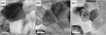
We sputtered ZnO seed layers at various RF powers (50–450 W) to systematically modulate the microstructure of a seed layer. Shown in Fig. 1 are TEM images obtained from some of the samples deposited at various RF powers and subsequently heated to 990 °C, the temperature at which nanowires were grown. The TEM images clearly demonstrate that the grain size of the films decreases with the RF power increasing, confirming that the final grain size is critically determined by the RF power used during deposition. This deposition power–grain size relationship could be explained by the fact that for films deposited at a high RF power, a high atomic flux would not provide the adsorbed atoms with sufficient time to diffuse and occupy the lattice sites of the growing grains, hampering grain growth, whereas for samples deposited at a low power, a low atomic flux would allow the grains to grow large.Reference Hwang, Park, Chun, An, Kim and Lee18
Plan-view transmission electron microscope (TEM) images of ZnO seed layers deposited at different RF powers after annealing at 990 °C: (a) 50 W, (b) 250 W, and (c) 450 W.

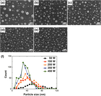
To investigate the effects of the microstructure of a ZnO seed layer on the distribution and size of Au catalytic particles, we deposited a thin Au layer (5-nm thick) on the ZnO seed layers grown at various RF powers and annealed using an identical thermal cycle used in the above-mentioned microstructure analyses of the ZnO seed layer, which led to the formation of nanometer-sized Au particles dispersed on the ZnO films, as shown in Fig. 2. Comparison of the images discloses a large variation in the distribution and size of the Au particles depending on the RF power of the ZnO seed layers. For the sample with the ZnO layer grown under 50 W, the Au particles are, overall, large in size and low in density. As the RF power increases, the Au particles become noticeably smaller and more densely populated. For quantitative analysis, we counted and plotted the number and size of the particles for each sample, as shown in Fig. 2(f). The graph clearly displays a systematic reduction in particle size with the RF power increasing. Another interesting feature displayed in the graph is that the distribution of the particle size is narrower for a ZnO layer deposited under a higher RF power. This apparent link between the RF power and Au particle distribution hints that the microstructure of the ZnO layers probably played a pivotal role in determining the Au particle distribution.
Scanning electron microscope (SEM) images of Au catalytic particles formed on the ZnO seed layers grown under different RF powers after annealing at 990 °C: (a) 50 W, (b) 150 W, (c) 250 W, (d) 350 W, and (e) 450 W. The scale bar is 100 nm. (f) The size distribution of the Au particles obtained by analyzing several SEM images for each sample.

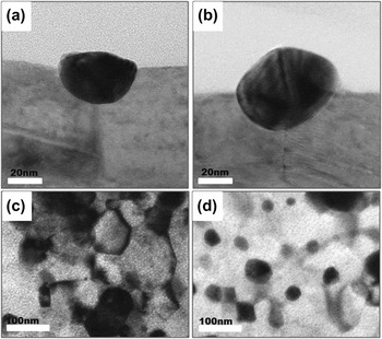
A close examination of the Au particles scattered on the ZnO seed layers using TEM shed some light on how the microstructure of the ZnO seed layers critically affects the distribution of the Au particles. TEM images shown in Figs. 3(a) and 3(b) display the cross-sectional morphology of the Au particles on the ZnO seed layers deposited at 50 and 450 W, respectively. For both samples, the morphology suggests that the Au layers agglomerated into nanoparticles preferentially along the grain boundaries of the seed layers, which possibly helped the formation of Au particles by offering energetically favorable sites. Furthermore, it seems that the Au particles grew deeply into the grain boundaries, which reflects the efforts of the particles to further reduce the surface energy by interacting with the underlying ZnO seed layer. These features emphasize the critical role of the grain boundaries of a seed layer in Au particle formation.
TEM images of Au particles formed on ZnO seed layers deposited at the RF power of (a, c) 50 W and (b, d) 450 W after annealing up to 990 °C: (a, b) cross-sectional images and (c, d) plan-view images.

Figures 3(c) and 3(d) show the electron micrographs taken from the plan-view samples of Au particles on ZnO seed layers deposited at 50 and 450 W, respectively, confirming the sensitive dependence of the Au particle distribution on the microstructure of a seed layer. For both the 50- and 450-W samples, the Au particles are positioned preferentially along the grain boundaries of the seed layers, consistent with the observation of the cross-sectional samples. The Au particles of the 450-W sample are small and scattered rather densely along the tightly networked grain boundaries of the ZnO layer deposited at 450 W, whereas those of the 50-W sample are large and distributed somewhat sparsely along the loosely networked grain boundaries of the ZnO layer grown at 50 W, highlighting the close relation between the microstructure of a seed layer and the Au particle distribution.
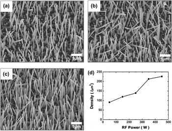
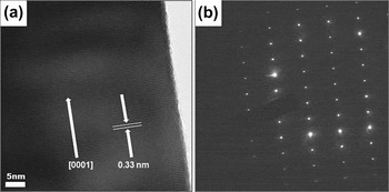
Next, we carried out the synthesis of ZnO nanowires on a ZnO seed layer covered with a catalytic Au layer by allowing the flow of Ar at 990 °C for 1 h, which led to the formation of Au catalytic particles and a subsequent nanowire growth. The growth morphology and microstructure of such nanowires are shown in Figs. 4 and 5, respectively. The nanowires appear grown straight and display a diameter in the range of 60–90 nm and a length greater than 5 μm. HR-TEM image acquired from such a nanowire, shown in Fig. 5(a), reveals the details of the microstructure of the nanowires. The nanowires are single crystalline and grew dominantly along the [0001] direction, as shown in the high resolution image and the selected area diffraction pattern (Fig. 5).
SEM images of ZnO nanowires grown on ZnO seed layers deposited at (a) 50 W, (b) 250 W, and (c) 450 W. The scale bar is 1 μm. (d) The ZnO nanowire densities were estimated from the SEM images for each sample.

(a) High resolution TEM image of a ZnO nanowire grown on ZnO seed layer deposited at a sputtering power of 450 W. (b) Selected area diffraction pattern along the zone axis of  , which clearly indicates the single crystalline growth of ZnO nanowire.

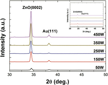
The SEM images of Fig. 4 disclose that the nanowire density increased systematically as the sputtering power of the seed layer escalated. We estimated the density of the nanowires for each sample by counting the number of the nanowires from such SEM images, as shown in Fig. 4(d). The nanowire density increases significantly with the sputtering power, from 90/μm2 for the 50-W sample to nearly 250/μm2 for the 450-W sample. We also examined the densities of the nanowires using XRD, as shown in Fig. 6. In the XRD curves, the entire samples exhibit the dominant peak at a position corresponding to the (0002) reflection, confirming that the nanowires grew predominantly along the [0001] direction. It should be noted that the intensity of the (0002) peak systematically increases with the RF power escalating, demonstrating that the nanowires grew more densely on a ZnO layer deposited at a higher power. This result, paralleling with the SEM observation, underscores the strong influence of the sputtering power used for the deposition of a ZnO seed layer on the Au particle distribution and the density of subsequently grown nanowires.
X-ray diffraction (XRD) data obtained from ZnO nanowires grown on ZnO seed layers deposited at different RF powers (50, 150, 250, 350, and 450 W). Shown in the inset is XRD data obtained from the ZnO seed layers with an Au catalytic layer only (i.e., before the nanowires were grown).

This close link between the sputtering power and the nanowire density demonstrates that modulating the sputtering power for the deposition of a seed layer (and thus the grain size) influences the subsequent processes (Au particle formation and nanowire growth) and eventually determines the nanowire density. First, the deposition of ZnO layers at various sputtering powers produces ZnO layers with a different grain size. As the grain boundaries of a ZnO seed layer play a critical role in Au particle formation by offering preferential sites for the particle formation, the grain size immensely influences the distribution of Au particles, which in turn determines the nanowire density because the Au particles act as a catalyst for nanowire growth.
IV. CONCLUSIONS
The results of this study demonstrate that controlling the deposition power of a ZnO underlayer could be a powerful method to increase the density of ZnO nanowires. We sputtered a ZnO thin film at various RF powers to modulate the microstructure, followed by the deposition of an Au catalytic layer and the growth of nanowires. We examined the samples after the key steps using SEM, TEM, and XRD to disclose that modulating the sputtering power for the deposition of the seed layer (and thus the grain size) influenced the subsequent processes (Au particle formation and nanowire growth) and eventually determined the nanowire density.
ACKNOWLEDGMENT
This work was supported by National Research Foundation of Korea Grant funded by the Korean Government (2010-0558000).