Introduction
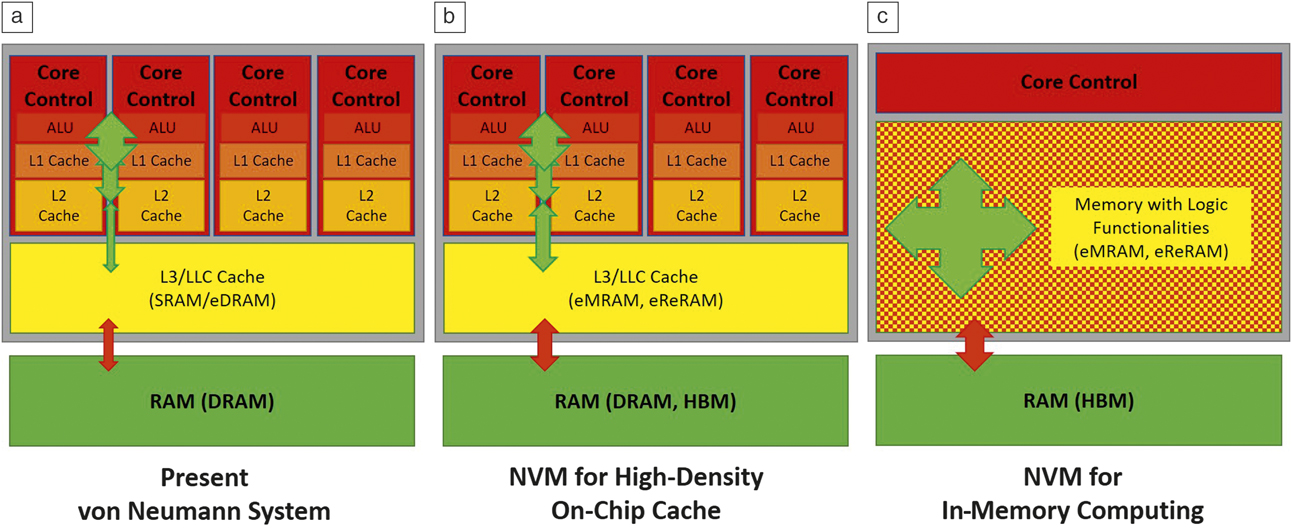
Static random-access memory (SRAM) technology is widely used today for on-chip registers and cache memory in modern microprocessors because of its fast access times (<1 ns) and extremely high endurance (>1015 read/write cycles). However, SRAM density is limited and its static power dissipation and cell size (in terms of F 2, where F is the feature size) continue to increase. Thus nearly all high-density working memories (dynamic random-access memory [DRAM]) are off-chip with high energy cost and slow access speeds, the latter of which has been historically known as the memory wall or von Neumann bottleneck (Figure 1a).Reference Wulf and McKee1
Computing systems architectures at present and in the future, only including computation chip and main memory (random-access memory, [RAM]). The arrow width indicates the bandwidth of data communication between adjacent memory layers. The green arrows indicate higher on-chip bandwidth over off-chip bandwidth of the red arrows. (a) Present von Neumann architecture.Reference Wulf and McKee1 (b) Use of nonvolatile memory (NVM) for high-density on-chip cache.Reference Fujita, Noguchi, Ikegami, Takeda, Nomura and Abe2 The high bandwidth memory (HBM) is also included in the RAM. (c) Use of memory with logic functionalities for in-memory computing paradigm.Reference Zidan, Strachan and Lu3 HBM is envisioned to replace dynamic random-access memory (DRAM) for the main memory. Note: ALU, arithmetic logic unit; L1 cache, first-level cache; L2 cache, second-level cache; L3 cache, third-level cache; LLC, last-level cache; eReRAM, embedded resistive random-access memory; eMRAM, embedded magnetic random-access memory; eDRAM, embedded dynamic random-access memory; SRAM, static random-access memory.

The situation is further exacerbated with the advent of big data and artificial intelligence, which demand fast access to large amounts of data at high processing speeds. One solution is to use high-density nonvolatile memory (NVM) with increased on-chip capacity to minimize access to the distant off-chip DRAM through the central processing unit (CPU)/DRAM bus, thus improving the system-level latency and energy performance. As illustrated in Figure 1b, with a much smaller cell size than SRAM, emerging high speed and endurance NVM technologies have the potential to implement nonvolatile on-chip cache with higher density.Reference Fujita, Noguchi, Ikegami, Takeda, Nomura and Abe2 Another more aggressive solution would be to use NVM cells as storage elements with logic functionalities (in memory computing),Reference Zidan, Strachan and Lu3 thus eliminating standby power consumption and enabling instant-ON operation, as shown in Figure 1c. This class of NVM will therefore become a strong candidate to realize novel computing paradigms that are energy efficient, nonvolatile, memory centric, and highly parallel.
Magnetic random-access memory (MRAM) that utilizes collective spin phenomena, originating from spin–orbit coupling (SOC), to store information is one of the most promising NVM candidates in this class. To date, almost all magnetic memories use the magnetic tunnel junction (MTJ) as the basic building block. As illustrated in Figure 2a, a MTJ mainly consists of a strong and fixed magnetic layer (CoFeB), and a weak and free magnetic layer (CoFeB) sandwiched by a thin tunneling barrier MgO. The energy barrier separating the two stable states of the free layer is defined as its magnetic anisotropy. The readout is achieved by measuring the tunneling magnetoresistance ratio (TMR) of the parallel (R P) and antiparallel (R AP) states, and the TMR is defined as (R AP-R P)/R P. In most MRAM types today, the switching of the magnetic free layer state is realized by passing a current through the MTJ stack. For example, in spin–transfer torque MRAM (STT-MRAM), the write is performed by passing a current to transfer the spin momentum of polarized electrons inherited from the fixed layer to the free layer.Reference Slonczewski4,Reference Sun5 Spin–orbit torque MRAM (SOT-MRAM) operates by passing a current through a high SOC material layer that will generate spin accumulation originating from the spin Hall or Rashba effect to switch the adjacent free magnetic layer.Reference Miron, Gaudin, Auffret, Rodmacq, Schuhl, Pizzini, Vogel and Gambardella6,Reference Liu, Lee, Gudmundsen, Ralph and Buhrman7
(a) Schematic of a magnetoresistance (R MTJ) plot of a voltage-controlled magnetic tunnel junction (V-MTJ) under a perpendicular magnetic field (H perp), measured when different voltages are applied. The R MTJ-H perp loops under voltages V 1 and V 2 are presented by red and blue colors, respectively. The insets show schematics of V-MTJ consisting of a fixed layer (white arrow pointing up in a fixed orientation), a free layer (white arrow can point to any one of the two orientations), and a tunnel barrier in between. The high resistance-area (RA) product V-MTJ has a thicker tunnel barrier than spin transfer torque (STT) MTJ, thereby enabling the voltage-controlled magnetic anisotropy (VCMA) effect to dominate over STT. When a positive (negative) voltage V 1 (V 2) is applied, the free layer magnetization indicated by the bidirectional white arrow tends to lie preferably in-plane (perpendicular). The positive and negative charges when the voltage is applied are drawn at the barrier surface. (b) Schematic showing the process of writing a bit using the VCMA effect, as illustrated by the energy landscape of the magnetic free layer as a function of the free layer angle θFL (indicated in [c]): (i) Before applying voltage, the free layer energy landscape has two stable energy minima at perpendicular orientations. Here, we designate the free layer angle of 90° to represent a bit value of “1”. (ii) Upon applying a positive voltage pulse, the free layer exhibits in-plane anisotropy, and the energy landscape has a minimum at a 0° free layer angle. Then, the free layer undergoes a precessional switching process under an in-plane bias magnetic field. The voltage pulse is timed to be half of the free layer precession period. (iii) The free layer angle will equal –90° after removing the voltage, representing a bit value of “0.” (c) Free layer magnetization m precession trajectory during the VCMA pulse. Heff refers to total effective magnetic field that mainly consists of the built-in or applied in-plane bias magnetic field, and θFL refers to the free layer angle with respect to the in-plane direction. To achieve switching from bit “1” to bit “0” as shown in (b), the time difference between t 1 and t 2 is half of the free layer precession period. (d) Schematic of a V-MTJ resting on a metal electrode with high spin–orbit coupling, which can generate spin–orbit torque (SOT) onto the MTJ when a current I SOT is passed, while the VCMA voltage (V VCMA) facilitates the switching by lowering the energy barrier. Note: R P (R AP), parallel (antiparallel) resistance of a MTJ when the free layer orientation is parallel (antiparallel) to the fixed layer.Reference Alzate22

On the other hand, for voltage write, magnetoelectric random-access memory (MeRAM) uses the voltage-controlled magnetic anisotropy (VCMA) effect,Reference Wang and Amiri8–Reference Maruyama, Shiota, Nozaki, Ohta, Toda, Mizuguchi, Tulapurkar, Shinjo, Shiraishi, Mizukami, Ando and Suzuki10 and this is the subject of discussion for this article. Using voltage/electric-field manipulation, which is free of ohmic loss, VCMA has been investigated as a next-generation MRAM for its lower switching current and higher density compared with current-controlled devices utilizing STT or SOT. Thus, MeRAM is much more scalable at complementary metal oxide semiconductor (CMOS) advanced nodes.
As illustrated in Table I, among emerging embedded NVMs, including embedded resistive random-access memory (eReRAM), STT-MRAM, SOT-MRAM, and MeRAM, MeRAM possesses the closest dynamic performance to SRAM and embedded DRAM (eDRAM) for use as cache memories on the central processing unit (CPU) chip.Reference Li11–Reference Lee, Lee, Ebrahimi, Amiri and Wang15 In a simple estimate based on the state of the art, MeRAM also has 6× higher density compared with SRAM in advanced nodes and approximately 2× density improvement over eDRAM. Its inherent high endurance, fast write speed, and CMOS backend-of-the-line process compatibility make it best positioned to serve as an on-chip memory solution.
Comparison of existing, prototypical, and emerging embedded memory technologies.

For each, data are averaged values based on several of the most advanced technology nodes. All data except the energy values indicated with * refer to a single cell, without considering the bit lines and peripheral circuits. Other data for magnetoelectric random-access memory (MeRAM) are simulated array-level projections based on device-level data.Reference Li11–Reference Lee, Lee, Ebrahimi, Amiri and Wang15 Note: eFlash, embedded flash; eReRAM, embedded resistive random-access memory; eDRAM, embedded dynamic random-access memory; STT-MRAM, spin transfer torque magnetic random-access memory; SOT-MRAM, spin–orbit torque magnetic random-access memory; SRAM, static random-access memory; F, feature size.
Voltage-controlled magnetic anisotropy
MeRAM employs a voltage-controlled MTJ (V-MTJ) with a thicker tunnel barrier than that in a STT-MRAM cell to suppress the tunneling current. Therefore, the capacitive characteristics of the tunnel barrier will dominate the write process through the modification of the magnetic anisotropy of the free layer through SOC (i.e., the VCMA effectReference Maruyama, Shiota, Nozaki, Ohta, Toda, Mizuguchi, Tulapurkar, Shinjo, Shiraishi, Mizukami, Ando and Suzuki10), as shown in Figure 2a.
The fundamental principle behind the VCMA effect is SOC as previously mentioned—the collective spins and magnetism are coupled to the electron orbital motion around a nucleus. More sophisticated theory indicates there are generally two physical causes of the VCMA effect. First, upon application of the voltage, charge accumulation or depletion at the ferromagnet/insulator interface will modify the electron occupancy of d orbitals of different symmetries of the magnetic layer at the interface. As these different electron orbitals possess different magnetic anisotropies due to SOC, the applied voltage can thus modulate the total magnetic anisotropy.Reference Duan, Velev, Sabirianov, Zhu, Chu, Jaswal and Tsymbal16 Second, the applied voltage can induce changes in the energy separation of the spin–orbit coupled pairs of occupied and unoccupied states of different symmetries, which will result in a change of the constituent magnetic anisotropy term that is inversely proportional to the energy separation.Reference Nakamura, Shimabukuro, Fujiwara, Akiyama, Ito and Freeman17
The effectiveness of the voltage control is characterized by the VCMA coefficient ξ = ΔK i/ΔE, a measure of how effective an applied voltage can alter magnetic anisotropy, where ΔK i is the interfacial anisotropy energy (K i) modulation induced by the applied electric field, ΔE, across the MTJ tunnel barrier. Thus, the higher ξ is, the lower will be the voltage and energy needed to switch the magnetic state. The role of the previously mentioned charge-induced VCMA effect has been confirmed experimentally by the increase of the VCMA coefficient when a composite tunnel barrier with a higher dielectric constant is used over simple MgO.Reference Chien, Li, Wong, Zurbuchen, Robbennolt, Yu, Tolbert, Kioussis, Amiri, Wang and Chang18 As the charge screening length in metals is on the order of Angstroms, the interface configuration of the ferromagnetic layer/tunnel oxide layer (CoFeB/MgO) is critical for ensuring a high VCMA coefficient. A clear correlation has been found where the over-oxidation of the CoFeB/MgO interface will result in a high VCMA coefficient.Reference Li, Fitzell, Wu, Ty Karaba, Buditama, Yu, Wong, Altieri, Grezes, Kioussis, Tolbert, Zhang, Chang, Amiri and Wang19 In addition, the epitaxial growth and resulting strain conditions as well as heavy-metal doping at the CoFe(Fe)/MgO interface can enhance the VCMA coefficientReference Kato, Yoda, Saito, Oikawa, Fujii, Yoshiki, Koi, Sugiyama, Ishikawa, Inokuchi, Shimomura, Shimizu, Shirotori, Altansargai, Ohsawa, Ikegami, Tiwari and Kurobe20,Reference Nozaki, Kozioł-Rachwał, Skowroński, Zayets, Shiota, Tamaru, Kubota, Fukushima, Yuasa and Suzuki21 of MTJs prepared by molecular beam epitaxy (MBE) or sputter-based solid-phase epitaxy on an MgO buffer.
MeRAM and magnetoelectric logic
MeRAM is written using precessional switching based on the VCMA effect. When the energy barrier is fully eliminated by the VCMA effect via an applied voltage (V A), and if there is an in-plane magnetic bias field built in (or applied to) the MTJ stack, the free layer magnetic moment will start precessional motion and oscillate between the up and down states until damping causes it to align with the bias in-plane field, as shown in Figure 2b–c.Reference Alzate22 Upon the removal of the voltage pulse, the magnetic state will return to its preferred up or down state as determined by the timing of the pulse. MeRAM devices with switching energies down to 6 fJ/bit and subnanosecond switching speeds have been demonstrated experimentally.Reference Grezes, Ebrahimi, Alzate, Cai, Katine, Langer, Ocker, Khalili Amiri and Wang23,Reference Kanai, Matsukura and Ohno24 For lower write energy and large density memory, a large ξ greater than 1000 fJ/V-m is desired, which will be discussed in the following section.
Apart from embedded memory replacement, MeRAM cells can be utilized for a variety of logic circuits. For example, today’s ternary content-addressable memory (TCAM) enables ultrafast fully parallel search operations; however, they employ SRAMs for storage, leading to large area (12∼16 transistors per cell) and significant standby power. By using MeRAM, a nonvolatile TCAM cell can be constructed with only four transistors and two MTJs, giving a 5× improvement in cell density with zero leakage power.Reference Lee25 Another example is lookup tables (LUT), which are the core components in programmable logic circuits. By resting the voltage-controlled MTJ upon a SOT metal electrode as shown in Figure 2d, the VCMA pulse selects the device to program by lowering the energy barrier, while the SOT bus exerts SOT onto the selected MTJ. This enables deterministic switching and parallel programming, where all bits that have the same to-be-written data can be written simultaneously. Compared to STT-based LUT, the configuration time is reduced up to 100× for six-input LUT, with 32% savings in area.Reference Lee, Ebrahimi, Amiri and Wang26
Voltage-controlled MeRAM cells can also serve as building blocks for novel computing paradigms. For example, stochastic computing processes information in the form of probabilities, represented in binary streams, and has the advantages of parallelization, error resiliency, and area efficiency, making it beneficial for applications such as artificial intelligence (learning and recognition) and informatics (sensor and social networks). One major challenge in stochastic computing is the generation of a true random bit stream (no correlation exists between each bit) with different probabilities. With the VCMA-on-SOT structure shown in Figure 2d, as VCMA drives the MTJ into a metastable state, current flowing through the SOT material simultaneously injects spin torque into the MTJ, biasing the switching probability proportional to the amplitude and polarity of the current.Reference Lee, Lee, Ebrahimi, Amiri and Wang27 A 3× to 37× energy improvement has been demonstrated compared with CMOS bit-stream generators.Reference Wang, Pal, Li, Pan, Grezes, Khalili-Amiri, Wang and Gupta28 An integrated MeRAM structure with SOT assisted writing has also been proposed to implement in-memory computing, where logic operations can be applied on the MTJ state without an intermediate readout of the device.Reference Zhang, Kang, Wang, Wang and Zhao29,Reference Baek, Park, Kil, Jang, Park, Lee and Park30
Challenges and perspectives
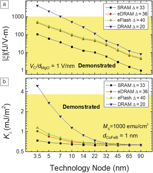
The demand for high density, high speed, and low energy memory will clearly continue to grow as our appetite for data-storage capacity and processing performance keeps increasing. MeRAM and related voltage-controlled memory and logic thus need to scale with the CMOS advanced nodes in terms of array density and energy. There are two so-called “1000” challenges. The most critical parameter is the VCMA coefficient, ξ. We carried out a detailed scaling analysis showing that the VCMA coefficient is inversely proportional to the square of the MTJ diameter.Reference Li11 As shown in Figure 3a, for MeRAM to replace SRAM, embedded flash (eFlash), and eDRAM at the 3.5-nm CMOS technology node, a VCMA coefficient of >1000 fJ/V-m is required.Reference Li11 The interfacial perpendicular magnetic anisotropy (PMA), K i, has a much less steep scaling slope than the VCMA coefficient, and a K i value of 1.2 mJ/m2 is sufficient for the 3.5-nm node, as seen in Figure 3b.Reference Li11,Reference Chung, Kishi, Park, Yoshikawa, Park, Nagase, Sunouchi, Kanaya, Kim, Noma, Lee, Yamamoto, Rho, Tsuchida, Chung, Yi, Kim, Chun, Oyamatsu and Hong31 Another important parameter is TMR. A large TMR greater than 1000% is needed to warrant a readout with large signal-to-noise ratio for large arrays. While implementing MeRAM as an embedded application integrated into the CMOS back-end-of-line process, the VCMA, PMA, and TMR properties need to preserve under annealing temperatures of 400–500°C. In addition, any deterministic writing scheme based on VCMA is highly desired.
(a) Voltage-controlled magnetic anisotropy (VCMA) coefficient (ξ) and (b) interfacial perpendicular magnetic anisotropy (K i) scaling trend over different complementary metal oxide semiconductor technology nodes for magnetoelectric random access memory to replace various technologies with different requirements of thermal stability (Δ), which is defined as ratio of the energy barrier between bit “1” and “0” over the thermal energy given by k BT, where k B is the Boltzmann constant and T is the memory operation temperature. We assume the critical switching voltage V C over MgO thickness d MgO equals 1 V/nm. The saturation magnetization M S of the CoFeB free layer is 1000 emu/cm3, and the thickness of the CoFeB free layer d CoFeB is 1 nm.Reference Grezes, Ebrahimi, Alzate, Cai, Katine, Langer, Ocker, Khalili Amiri and Wang23 For both figures, the size of the magnetic tunnel junction (MTJ) cell to replace static random-access memory (SRAM), embedded dynamic random-access memory (eDRAM), and embedded flash (eFlash) equals 1/6 of a SRAM cell at the same node, while the size of the MTJ cell to replace DRAM is the same size as a DRAM cell. We also assume the MTJ diameter equals half of the MTJ cell length side in the scaling analysis.Reference Chung, Kishi, Park, Yoshikawa, Park, Nagase, Sunouchi, Kanaya, Kim, Noma, Lee, Yamamoto, Rho, Tsuchida, Chung, Yi, Kim, Chun, Oyamatsu and Hong31 The yellow shaded regions refer to VCMA and interfacial perpendicular magnetic anisotropy values demonstrated in experiments. Reprinted with permission from References Reference Kato, Yoda, Saito, Oikawa, Fujii, Yoshiki, Koi, Sugiyama, Ishikawa, Inokuchi, Shimomura, Shimizu, Shirotori, Altansargai, Ohsawa, Ikegami, Tiwari and Kurobe20 and Reference Nozaki, Koziol-Rachwal, Tsujikawa, Shiota, Xu, Ohkubo, Tsukahara, Miwa, Suzuki, Tamaru, Kubota, Fukushima, Hono, Shirai, Suzuki and Yuasa32. © 2018 and 2017 IOP Publishing and Nature Publishing Group, respectively.

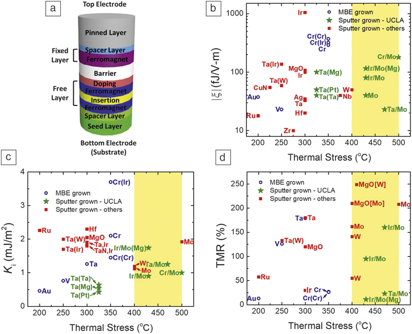
Summary plots of recent VCMA, PMA, and TMR experimental work for perpendicular MTJsReference Li11 are shown in Figure 4b–d. Figure 4a shows the standard MTJ structure, including seed/spacer layers beneath the ferromagnet/barrier/ferromagnet stack, doping layers at the ferromagnet/barrier interface, and insertion layers in the ferromagnet free layer. From Figure 4b, we can see that a VCMA coefficient of around 1000 fJ/V-m is possible by sputtering a CoFe/MgO bilayer structure on Ta/CoFeB/MgO/Cr/Ir seed followed by annealing at 300°C,Reference Kato, Yoda, Saito, Oikawa, Fujii, Yoshiki, Koi, Sugiyama, Ishikawa, Inokuchi, Shimomura, Shimizu, Shirotori, Altansargai, Ohsawa, Ikegami, Tiwari and Kurobe20 while the highest interfacial PMA (K i) demonstrated in the Cr/Fe/Ir/MgO structure is 3.7 mJ/m2 (Figure 4c).Reference Slonczewski4,Reference Nozaki, Koziol-Rachwal, Tsujikawa, Shiota, Xu, Ohkubo, Tsukahara, Miwa, Suzuki, Tamaru, Kubota, Fukushima, Hono, Shirai, Suzuki and Yuasa32 These two values can already enable MeRAM replacement of SRAM/eDRAM/eFlash down to the 3.5-nm node.Reference Li11
(a) Schematic of a voltage-controlled magnetic tunnel junction (V-MTJ) stacks with different layers. (b) Published experimental results of voltage-controlled magnetic anisotropy (VCMA) coefficient ξ, (c) interfacial perpendicular magnetic anisotropy K i, and (d) tunneling magnetoresistance ratio (TMR) for different seed/spacer/insertion/doping materials as a function of thermal stress temperature in perpendicular MTJs.Reference Li11 The blue open circles refer to V-MTJ stacks grown by molecular beam epitaxy (MBE), the green and red points refer to those grown via sputtering. The labels beside each data point indicate the seed/spacer material used, the parentheses indicate the doping material between the free layer and tunnel barrier, while the bracket indicates the insertion material in the free layer that is sandwiched by two tunnel barriers. The yellow regions refer to annealing temperatures incurred during the complementary metal oxide semiconductor (CMOS) back-end-of-the-line (BEOL) processing. Though significant progress has been made in achieving high VCMA coefficient and interfacial perpendicular magnetic anisotropy, MTJ materials able to sustain these CMOS BEOL annealing temperatures are a prerequisite for adopting magnetoelectric random-access memory as an industrial embedded memory solution.Reference Li11

The low-k dielectrics (k is the dielectric constant) used between interconnects require a thermal budget greater than 400°C during advanced CMOS back-end-of-line processes, hence it is critical that the VCMA coefficient, PMA, and TMR can survive under high-annealing temperatures above 400°C. There has been much materials research done for preserving VCMA/PMA/TMR properties under high annealing temperatures for embedded applications by incorporating a Mo/W spacer between the seed layers and the CoFeB free layer.Reference Li11,Reference Li, Yu, Wu, Ong, Wong, Hu, Ebrahimi, Upadhyaya, Akyol, Kioussis, Han, Amiri and Wang33–Reference Wang, Cai, Cao, Zhou, Wrona, Peng, Yang, Wei, Kang, Zhang, Langer, Ocker, Fert and Zhao36 By combining the previously mentioned new materials design with a thermal barrier such as Mo and W, it is possible to realize high VCMA, PMA, and TMR that are also thermally stable above 400°C.Reference Li11
It is worth noting that (as seen in Figure 4d) high TMR of approximately 200∼250% can be realized for perpendicular MTJs with thermal annealing temperatures greater than 400°C. For in-plane MTJs, the maximum TMR at room temperature can reach a much higher 604% after annealing at 500°C. Because the thicker in-plane free layer (6-nm CoFeB) is more robust against elemental diffusion, during annealing, in-plane MTJs can achieve higher crystallization quality, and thus higher TMR after annealing.Reference Ikeda, Hayakawa, Ashizawa, Lee, Miura, Hasegawa, Tsunoda, Matsukura and Ohno37 Fortunately, new demonstration shows sub-20-nm diameter perpendicular MTJs using thick free layers (15-nm FeB)Reference Watanabe, Jinnai, Fukami, Sato and Ohno38 that can potentially further improve perpendicular TMR values. However, compared to the 105 ON-OFF ratio of CMOS technology, the low TMR generic to all MRAM based on MTJ poses a major limitation of a low read margin as well as the requirement of sophisticated sense amplifier circuitries.Reference Zhang, Li, Sun, Li, Chen and Jones39,Reference Lee, Grèzes, Wang, Ebrahimi, Gupta, Amiri and Wang40
There are two main ways to increase TMR. One is to increase the spin polarization of the ferromagnetic layers. For example, a half-metal acts as a metal for one spin orientation, but it shows insulating or semiconducting properties for the opposite spin orientation. In principle, the spin-polarization of a half-metal can ideally reach 100% and the TMR can be very high. Heusler alloys, which are ternary magnetic intermetallic compounds with a face-centered-cubic crystal structure, have attracted much interest because of their theoretically predicted half-metallicity and Curie temperatures well above room temperature. For CoFeMnAl Heusler alloy structures, the TMR can reach 2610% at 4.2 K.Reference Liu, Kawami, Moges, Uemura, Yamamoto, Shi and Voyles41 Another avenue is to use alternative barrier materials, such as the recently reported van der Waals spin-filter barrier, where an atomically thin two-dimensional ferromagnet chromium triiodide (CrI3) acts as a spin-filter tunnel barrier sandwiched between graphene contacts. When the CrI3 transitions from ferromagnetic to antiferromagnetic order, due to the spin-filter effect, the TMR can reach 19,000% at 2 K.Reference Song, Cai, Tu, Zhang, Huang, Wilson, Seyler, Zhu, Taniguchi, Watanabe, McGuire, Cobden, Xiao, Yao and Xu42 As standard CoFeB/MgO/CoFeB-based MTJs show 1160% TMR at 5K and 604% TMR at room temperature,Reference Ikeda, Hayakawa, Ashizawa, Lee, Miura, Hasegawa, Tsunoda, Matsukura and Ohno37 for both the previously mentioned avenues, high TMRs at room temperature are possible and further research into the materials is desired.
Apart from the previously mentioned materials requirement for high VCMA/PMA/TMR values, the successful adoption of magnetoelectric devices using voltage-controlled MTJs requires a sufficiently low bit error rate of 10–9. The precessional switching method based on VCMA previously described requires precise control of the applied voltage pulse and is nondeterministic, resulting in relatively high write error rates (WER). In order to achieve WER of 10–9, one can utilize multiple read/write cyclesReference Grezes, Lee, Lee, Wang, Ebrahimi, Li, Wong, Katine, Ocker, Langer, Gupta, Amiri and Wang43 and a write pulse with closer-to-square shape.Reference Lee, Lee, Wang, Ebrahimi, Gupta, Amiri and Wang44 The use of MTJs with higher thermal stability and optimal in-plane bias field has been shown to reduce single-pulse WER down to around 10–5.Reference Shiota, Nozaki, Tamaru, Yakushiji, Kubota, Fukushima, Yuasa and Suzuki45
Alternatively, because the VCMA effect temporarily lowers the energy barrier, it can be combined with other deterministic switching mechanisms for lower energy consumption (e.g., STT and SOT). For example, using a first large voltage pulse that induces magnetization precession via the VCMA effect and a second small voltage pulse that stabilizes the magnetization direction by STT, VCMA-assisted STT switching can realize deterministic, fast, and energy-efficient switching.Reference Kanai, Nakatani, Yamanouchi, Ikeda, Sato, Matsukura and Ohno46 SOT is another current-induced switching mechanism that has recently been made deterministic by using exchange biasReference Fukami, Zhang, DuttaGupta, Kurenkov and Ohno47 or structural asymmetries,Reference Yu, Upadhyaya, Fan, Alzate, Jiang, Wong, Takei, Bender, Chang, Jiang, Lang, Tang, Wang, Tserkovnyak, Amiri and Wang48 which can also be used in combination with VCMA for deterministic switching, with the advantage of having faster speeds and potentially higher energy efficiency compared to STT. On the other hand, SOT devices require three terminals and thus have lower density. This problem can be mitigated by using a shared SOT bus across multiple MTJs.Reference Yoda, Shimomura, Ohsawa, Shirotori, Kato, Inokuchi, Kamiguchi, Altansargai, Saito, Koi, Sugiyama, Oikawa, Shimizu, Ishikawa, Ikegami and Kurobe49
Another approach for reducing the write error rate in VCMA switching utilizes skyrmions, which are vortex-like spin textures, in an intermediate step.Reference Bhattacharya and Atulasimha50 Under a VCMA pulse, the anisotropy of the ferromagnet changes, and a skyrmion phase can be created and will undergo oscillatory shrinking and expanding phases. Removing the voltage pulse during the shrinking phase results in magnetization reversal without the need of any external magnetic field. This skyrmion-mediated VCMA switching approach does not necessarily result in a fully deterministic VCMA switching and still requires control of the voltage pulse width. Researchers may find additional pathways to yield much lower write error rates.
Conclusion
VCMA-based magnetoelectric devices or MeRAM, have emerged as a next-generation high-speed and endurance, low-energy, and high-density solution for both on-chip cache and various big data-driven computing applications. Research on materials towards achieving a high VCMA coefficient will be instrumental for ensuring continuous scaling of this new technology. Using solid-phase epitaxial growth and thermal barrier spacers, VCMA can potentially exceed 1000 fJ/V-m while being compatible with CMOS back-end-of-line processing temperatures of approximately 400°C. Likewise, it is desirable to achieve TMR higher than 1000%. To this end, the exploration of Heusler alloy-based free layers as well as new barrier materials has the potential to address the low readout TMR challenge. Furthermore, by adopting new circuit-level and device-level operation schemes, the write error rate challenge due to the precessional switching of VCMA-based devices could be eliminated.

Xiang (Shaun) Li is currently a postdoctoral researcher in the Materials Science and Engineering Department at Stanford University. He received his PhD degree in electrical and computer engineering from the University of California, Los Angeles (UCLA) in 2018. He received his BS degree in physics at Peking University, China, in 2013. His research interests focus on novel magnetic materials and devices for memory-intensive applications, neuromorphic architectures, and technology commercialization. He was a Technology Fellow with the UCLA Technology Development Group and was responsible for technical partnership and investor development at Inston Inc., a UCLA spin-off startup. Li can be reached by email at xiangsli@stanford.edu.

Albert Lee is currently a doctoral candidate in the Electrical and Computer Engineering Department at the University of California, Los Angeles. He received his BS and MS degrees in electrical engineering from National Tsing Hua University, Taiwan. His research interests include nonvolatile logic, emerging nonvolatile memory, and neuromorphic circuits and their application to developing new machine-learning algorithms. Lee can be reached by email at alee0618@g.ucla.edu.

Seyed Armin Razavi is a doctoral candidate in the Electrical and Computer Engineering Department at the University of California, Los Angeles. He obtained his BS degree from Sharif University of Technology, Iran, in 2014. His research focuses on the intersection of electrical engineering, applied physics, and materials science. His research interests include nanomagnetism and spintronics device physics based on ferromagnets, antiferromagnets, heavy metals, and topological insulators. Razavi can be reached by email at arvinrazavi@gmail.com.

Hao Wu is a postdoctoral researcher in the Electrical and Computer Engineering Department at the University of California, Los Angeles. He received his PhD degree in condensed-matter physics from the Institute of Physics, Chinese Academy of Sciences, China, in 2017. His research interests include magnetic heterostructures and nanodevices, spin Hall-related phenomena, spin–orbit torque from topological insulators, and spin transport in magnetic insulators. Wu can be reached by email at wuhaophysics@ucla.edu.

Kang L. Wang is the Distinguished Raytheon Chair Professor at the University of California, Los Angeles, in the Departments of Physics, Electrical and Computer Engineering, and Materials Science and Engineering. He received his BS degree from National Cheng Kung University, Taiwan, and his MS and PhD degrees from the Massachusetts Institute of Technology. His awards include the IUPAP Magnetism Award and Néel Medal, the IEEE J.J. Ebers Award for electron devices, SRC Technical Excellence Award, and the Pan Wen-Yuan Award. He is a Guggenheim Fellow, a Fellow of the American Physical Society and IEEE, a Laureate of the Industrial Technology Research Institute of Taiwan, and an Academician of Academia Sinica. His research interests include spintronics and nonvolatile electronics, topological insulators and condensed matter, and molecular beam epitaxy. Wang can be reached by email at wang@seas.ucla.edu.