I. INTRODUCTION
The auto interference effects like cross-talk and dispersion of the digital wired interconnects limit the capacity of the on-chip and chip-to-chip communication channels. Wireless interconnects, based on CMOS radio frequency (CMOS RF) front-ends and on-chip integrated antennas, have a potential to overcome the bandwidth limitations of the wired communication links. CMOS RF circuits with operating frequencies up to 80 GHz belong to the state of the art [Reference Cao and O1–Reference Wang and Wang4]. The integration of antennas in silicon monolithic integrated millimeter-wave circuits (SIMMWICs) with high-resistivity substrate has already been described in the literature [Reference Russer, Biebl, Luy and Russer5, Reference Russer6]. The restrictions in on-chip integrated antenna design are due to the cost of the chip area and the losses in the low-resistivity substrate, used in CMOS technology. Monolithic integrated antennas, published in the literature, include linear, meander, and zigzag dipoles, loop antennas [Reference Kim and O7, Reference Kim, Yoon and O8], and planar inverted-F antennas [Reference Chan, Chin, Chen, Lin, Duh and Lin9]. These antenna types require considerable area on the chip and exhibit narrow frequency bandwidth. Kikkawa et al. have investigated the behavior of fractal antennas, integrated on silicon substrates [Reference Kikkawa, Kimoto and Watanabe10], which showed wide-band characteristics, but at the cost of considerable chip area. Mendes et al. have deposited high-resistivity polycrystalline silicon on the chip used as the substrate for a patch antenna [Reference Mendes, Sinaga, Polyakov, Bartek, Burghartz and Coreia11]. This approach saves chip area, as the antenna is placed above the circuit layers, but the frequency bandwidth provided is quite narrow.
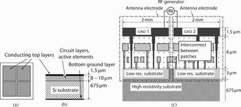
The approach, proposed in this work, is based on the sharing of chip area between the integrated circuit and the antenna [Reference Yordanov and Russer12]. This is achieved by subdividing the CMOS circuit ground plane into parts and using these parts as antenna electrodes. The circuits have to be designed in such a way that the ground layer of the power supply circuitry is implemented on the top-most metallic layer. Figure 1(a) shows the top view and Fig. 1(b) shows the cross section of the circuit structure. Figure 1(c) presents a detailed view of the interconnection layers of the integrated circuit. The metallic top layer with 1.5 µm thickness serves as the local ground layer for the electronic circuit underneath. Under this top layer is located a layer with a thickness of 8–10 µm, containing the active elements, embedded in low-resistivity silicon, and the metallic interconnects. The silicon substrate of 675 µm thickness has a resistivity of 1000 Ω cm or more. The bottom of the chip is continuously covered by a bottom ground layer. The top layer is subdivided into patches, as shown in Fig. 1. DC supply of the circuits under the patches and ground connection of the patches is performed via inductive blocks. If two patch areas (this includes the patches as well as the circuitry under the patches) are connected by a number of n interconnect wires, this bundle of wires carries n−1 transmission line modes and one antenna mode [Reference Russer13]. For any transmission line mode the total current flowing through all the interconnects is zero, whereas the total current flowing through all interconnects between two patches is the antenna current exciting the respective pair of patches as an antenna. The field excited by the antenna mode excitation extends over the whole thickness of the substrate and only minor parts of the fields are stored in the low-resistivity layer; therefore, the losses due to the low-resistivity substrate are limited and the antenna modes are weakly coupled with the transmission line modes. Furthermore, the interference between circuit and antenna modes can be suppressed by using, for the wireless communication link, a frequency band above the operating frequency band used by the circuits. The proposed solution has the following advantages: it does not require additional chip area and it is cost efficient, since it can be realized with modified CMOS technology. The modification concerns the use of high-resistivity substrate and the limitation of low-resistivity epitactical layers for the active devices to a few micrometer thickness.
Top view (a) and cross section (b) of the proposed antenna structure. (c) Detailed view of the cross section of the integrated on-chip antenna, using the ground planes as antenna electrodes. The separated areas of the ground planes have to be connected to each other using inductive connections. The RF generator is also integrated in the CMOS circuit. The figure is not to scale.

II. VERIFICATION OF THE RADIATION PARAMETERS
In order to verify the radiation parameters of the proposed antenna structure, a benchmark case has been investigated and a scaled prototype has been manufactured and measured. Several assumptions have been made for this study. It has been assumed that the electronic circuit interconnects have no influence on the antenna radiation characteristics. The losses of the substrate have also been neglected. The feeding of the antenna has been realized using an external power generator. These assumptions allow for the investigation of the antenna parameters using a scaled prototype, manufactured on a high-frequency laminate instead of on silicon.
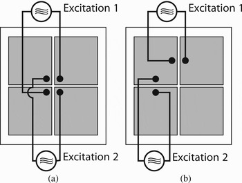
In the following, we investigate a structure consisting of four rectangular patches, placed in a 2 × 2 arrangement, as shown in Fig. 2. If the two sets of diagonally arranged patches are excited by two generators, as presented in Fig. 2(a), the resulting structure can be used as two separate antennas for a 2 × 2 MIMO channel. Another radiation regime can be generated by exciting the two sets of neighboring patches, as shown in Fig. 2(b). For this excitation the antenna exhibits a different resonant frequency.
Diagonal (a) and adjacent (b) antenna excitation.

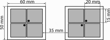
A 2 × 2 patch arrangement with patch dimensions of 20 × 15 mm2 with diagonal excitation, as shown in Fig. 3, has been investigated in order to analyze the antenna operating mode. The chosen substrate is RO4350BTM with ɛr = 3.48; therefore, this investigation does not account for the losses in the silicon substrate. The generator excites a wave, which propagates in the gap between the patches from the generator toward the antenna edges. When the wave reaches the end of the gap, it is reflected back, thus forming a standing wave pattern between the patches. The 15 mm length between the generator and the antenna edge will represent an open-circuited transmission line resonator with resonance frequency, corresponding to λg/2 = 15 mm, where λg is the guided wavelength. This corresponds to a frequency of

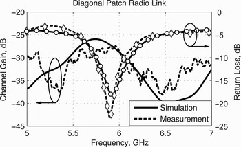
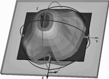
where c 0 is the velocity of light in free space. The effective dielectric permittivity of the transmission line is ɛ r,eff = 1/2(1 + ɛ r), because the electric field of the transmission line spreads over both the substrate underneath and in the free space above the metallization. Since the transmission line resonator, formed by the gap, is not terminated with a perfect open circuit, the effective length of the gap is a bit bigger and the resonant frequency of the resonator will be a bit greater than computed in (1). Performing the same computation for the other gap with length 20 mm, we obtain a resonant frequency of 5.01 GHz. The numerical results for the antenna return loss (Fig. 4) show a resonance, occurring at 5.9 GHz, which is between the two resonant frequencies of the gaps. The current distribution, presented in Fig. 5, shows the standing wave patterns. The radiation pattern of the antenna is shown in Fig. 6. The direction of maximum radiation in the plane of the patches is along the diagonal of the patches, i.e. at φ = −50° and 130°. The presented pattern is computed with only one set of diagonal patches excited. Both sets can be excited with two independent generators, e.g. for 2 × 2 MIMO channel (Fig 2(a)). In that case the coupling between the two patch sets will be severe, as seen in Fig. 7, and can degrade the MIMO channel performance.
Dimensions of the simulated and manufactured scaled antenna prototypes. Excitation points are marked.

Simulated and measured antenna return loss and channel gain of the configuration, presented in Fig. 3.

Surface current distribution at f = 6 GHz of the 2 × 2 patch structure from Fig. 3. Excitation points are marked.

Radiation pattern of the diagonally excited antenna from Fig. 3.


Two sets of the described antennas were manufactured and measured. A printed circuit wide-band balun [Reference Edward and Rees14] for the antenna feeding networks was manufactured. A sample link has been constructed. As in chip-to-chip communication near-field data links are of major interest, the distance between the receiver and the transmitter antenna was 35 mm (Fig 3). The simulated and measured antenna return loss and channel insertion loss are presented in Fig. 4.
III. THE INTERCONNECTS AND ANTENNA FEEDING
The discussion in the previous section neglected the influence of the electronic circuit interconnects. This assumption, as shown in [Reference Yordanov and Russer12], is justified for the interconnects, which are located underneath the antenna patches, but the interconnects, which connect the areas under separate patches (see Fig. 1(c)) have a severe effect on the input impedance. This can be understood as follows. The gap between the patches is very small (50 µm in our case); therefore, most of the electric energy of the antenna is concentrated in the vicinity of the gap between the two patches. Therefore, the radiation properties of the antenna emerge due to the standing wave, generated in the slot between the patches, which is fed with energy at one end and terminated with an open-circuit at the other end. Introducing the interconnection wire we effectively short-circuit this slot, thus perturbing the standing wave and changing the input impedance and the resonance frequency.
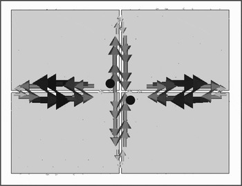
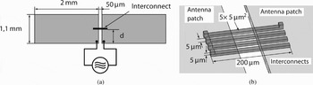
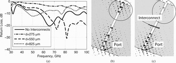
Consider, for example, a two-patch antenna, fabricated on a silicon substrate, with patch dimensions of 1.2 × 2 mm, as shown in Fig. 8(a). The resonance frequency of this antenna is 66 GHz. We have selected an operating frequency bandwidth with center frequency of 66 GHz for the following reasons: the state-of-the-art RF CMOS technology allows operation in that frequency range; the high operation frequency yields higher bandwidths and thus greater channel capacity; and the atmospheric attenuation due to the resonance of the oxygen molecules provides a smaller cross-talk between adjacent communication channels. Consider a four-wire interconnection bus, located at a distance d from the patch edge. The wire geometry is presented in Fig. 8(b). The interconnect has a length of 200 µm and each wire has a cross section of 5 × 5 µm2. The bus is positioned 5 µm below from the ground plane. The bus wires are connected to the ground plate on one side to account for the low output impedance of the CMOS stage and left open-circuited at the other end to account for the high input impedance. One of the wires is short-circuited on both ends, thus providing low-frequency connection between the two ground plates. Figure 9(a) compares the return loss of the antenna for different positions of the interconnection bus relative to the patch edge, as well as in the absence of interconnects. Figures 9(b) and 9(c) show a comparison of the field distribution in the gap between the patches in the presence and in the absence of an interconnection bus. The dimension of the arrows in these figures is proportional to the logarithm of the field magnitude. Note the difference in the marked areas.
(a) Top view of a double-patch antenna, operating at 66 GHz. (b) Geometry of the investigated interconnect.

(a) Influence on the reflection loss of an integrated antenna of a single line, connecting the areas between the two patches. Electric field distribution in the slot between the patches in the absence (b) and in the presence (c) of an interconnection wire.

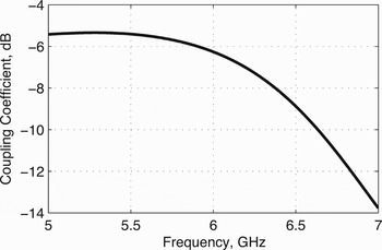
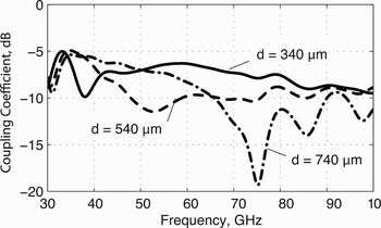
Another problem that arises due to the interconnection wires, located between two patches, is the coupling between the antenna mode and the transmission line modes. This leads to induced voltage on the interconnection bus, which can lead to noticeable bit error rate degradation. Using the model, described above, we can compute the coupling coefficient between the antenna and the interconnect. The result is presented in Fig. 10.
Coupling between antenna and interconnects for different values of the distance between the antenna port and the interconnect d (see Fig. 8(a)).

The discussion above has outlined three problems in the usage of the circuit ground planes as antenna electrodes: the influence of the cross-patch interconnects on the antenna field distribution; the coupling between the antenna mode and the transmission line modes; and the DC connection via inductors between different patches. These problems can be solved simultaneously by introducing a transformer in the feeding circuitry of the antenna. The principle of operation of such transformer is presented below.
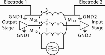
Consider a transformer with three windings, denoted by 1, 2, and 3, as shown in Fig. 11. The self-inductance of windings 2 and 3, as well as the mutual inductance between them M 23 are very small for the operational frequency of the CMOS circuit. The mutual inductance between windings 1 and 2 M 12, and between windings 1 and 3 M 13 are the same, i.e. M 12 = M 13. Winding 2 connects a digital circuit output stage to an input stage. Winding 3 connects the local CMOS circuitry ground planes, denoted by GND1 and GND2, which are also the two antenna patches. Therefore, windings 2 and 3 are a two-wire interconnection bus. An RF signal is fed to winding 1. Due to the mutual inductance M 13 the signal is coupled to winding 3, thus feeding the antenna. Since the mutual inductances M 13 and M 12 are equal, the RF voltage induced at the input of the input stage is the same as the RF voltage, induced at the reference ground of that stage, therefore there is no RF voltage drop at the input of the buffer. Similarly there is no RF voltage drop at the output of the output stage.
Principle schematic of antenna feeding with transformer.

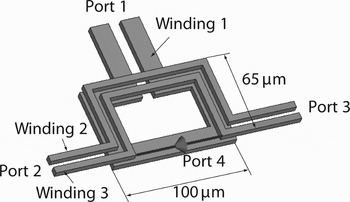
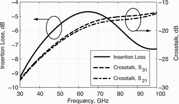
Figure 12 presents an implementation of the described principle. In order to make the mutual inductances M 13 and M 23 equal, the interconnection wires are of equal cross section and are placed symmetrically around the feeding winding. Winding 3 of the transformer is directly feeding the patch antenna, drawn schematically in Fig. 8(a). The patch antenna exhibits a resonance at 66 GHz. The dimensions of the transformer are 100 × 65 µm2. The cross section of the primary winding is 15 × 5 µm2. The cross section of the secondary windings is 5 × 5 µm2. The gap between all windings is 5 µm. The transmission line, constituted by windings 2 and 3, has a characteristic impedance of 40 Ω and electrical length of 82° at 66 GHz. The insertion loss between the feeding and the antenna input of this transformer, as well as the coupling to the input of the buffer, are presented in Fig. 13. It can be seen that the insertion loss is relatively big–about −4 dB, which is mostly due to impedance mismatch and due to the substrate losses, but this value is close to the reported values in other works [Reference Dickson, LaCroix, Boret, Gloria, Beerkens and Voinigescu15]. The coupling to the buffer input is quite low, as expected.
Feeding transformer.

Insertion loss and cross-talk coefficient between the antenna and the interconnects.

IV. CONCLUSIONS
In this work an integrated on-chip antenna has been presented. The antenna design is based on the sharing of chip area between the electronic circuits and the radiating elements. This has been achieved by subdividing the ground plane of the circuit into patches and using these patches as antenna electrodes. The interference between the antenna and the circuit has been minimized by introducing a transformer in the feeding network of the antenna, thus exciting interconnects in transmission line modes and the antenna electrodes in antenna modes. The computed radiation characteristics of the antenna have been verified experimentally using a scaled prototype.
ACKNOWLEDGEMENT
This work was supported by the Deutsche Forschungsgemeinschaft.
 Hristomir Yordanov received a B.Sc. degree in radio communications from Technical University of Sofia, Sofia, Bulgaria, in 2002 and an M.Sc. degree in microwave engineering from the Techische Universität München (TUM), Munich, Germany, in 2006. He is currently working toward his Ph.D. degree as a research assistant at Institute for High Frequency Engineering at TUM. His research areas include wired and wireless chip-to-chip and on-chip communications, small antennas, superdirectivity, and near-field communication.
 Peter Russer (F'94) received the Dipl.-Ing. and Dr. techn. degrees from the Vienna University of Technology, Vienna, Austria, in 1967 and 1971, respectively, both in electrical engineering. In 1971, he joined the Research Institute of AEG-Telefunken, Ulm, Germany. From 1981 to 2008 he has been a professor and Head of the Institute for High Frequency Engineering, Technische Universität München, Munich, Germany. From 1992 to 1995, he was the director of Ferdinand-Braun-Institut, Berlin, Germany. From 1997 to 1999, he was the dean of Department of Electrical Engineering and Information Technology, Technische Universität München. He has authored/coauthored over 670 scientific papers in refereed journals and conference proceedings. He has served as a member of the Editorial Board for several international journals. His current research interests include electromagnetic fields, numerical electromagnetics, metamaterials, integrated microwave and millimeter-wave circuits, statistical noise analysis of microwave circuits, time-domain measurement methods in EMC, and methods for computer-aided design of microwave circuits. He is a member of the German Informationstechnische Gesellschaft (ITG) and the German, as well as the Austrian Physical Societies. He is a member of the German Academy of Science and Engineering (ACATECH). He has served as a member of the Technical Program Committees and Steering Committees of various international conferences. In 1999, he was the general chairman of European Microwave Week, Munich, Germany. From 1999 to 2002, he was co-chair, and from 2002 to 2005, he was chair of the URSI Commission D. From 1999 to 2002, he was co-chair, and from 2002 to 2005, he was chair of the URSI Commission D. He is currently the chair of the IEEE Technical Committee MTT-15 Microwave Field Theory. In 2007, he was the president of the EMC Zurich Conference, Munich, Germany. He was the recipient of the 1979 NTG Award and of the 2006 Distinguished Educator Award presented by the IEEE Microwave Theory and Techniques Society (IEEE MTT-S). He received an honorary doctor degree in 2007 from the Moscow University of Aerospace Technologies (MAI).