I. INTRODUCTION
Wireless power transfer technology, such as inductive power transfer (IPT), has attracted the interest from academic and industrial worlds for its advantageous features to provide a safe and convenient way to supply power with galvanic isolation and movement freedom of the load. It has already found various applications such as material handling system [Reference Boys, Covic and Green1], electric vehicle charging [Reference Chwei-Sen, Stielau and Covic2, Reference Swain, Devarakonda and Madawala3], consumer electronics [Reference Hui and Ho4, Reference Hsu, Hu and Swain5], and implanted biomedical device charging [Reference Ping, Hu, Malpas and Budgett6]. Recently, capacitive power transfer (CPT), also termed as capacitively coupled power transfer (CCPT), is gaining acceptance as an alternative solution for wireless power transfer using the electric field as the power transfer medium in the form of two pairs or one single pair of coupling plates [Reference Hu, Chao and Hao Leo7–Reference Van Neste12]. It provides following advantageous features: low power losses, low electromagnetic interference (EMI), flexibility of coupling structure design, and the ability to transfer power through metal objects as long as the coupling electric field is not fully shielded. It can be potentially used in applications such as monorail trolleys and linear motors where metallic tracks exist on two separate sides. Figure 1 shows a typical CPT system which is comprised of a high frequency AC power source, a capacitive-coupling interface (usually formed by two pairs of coupling plates coated with dielectric materials), and a pickup circuitry which regulates the received power according to the requirement of the load. Among these parts, the capacitive-coupling interface is the heart of the system. Therefore, a good understanding of the coupling interface and its effect on the system performance is important for a proper design of a CPT system, necessitating an accurate model of the capacitive coupling. However, in real-world CPT systems, misalignment within the capacitive-coupling interface, even short distance between plates on the same side in small profile applications, may cause cross-coupling problem, making modeling and analysis of such systems not straightforward.
A typical CPT system.

In most CPT literature, the capacitive coupling is simply modeled as a pair of capacitors in series [Reference Liu, Hu and Nair13–Reference Liang, Hu, Swain, Seho and Yijun20]. This simple model is valid only when the coupling plates are well-aligned with each other as shown in Fig. 2(a). However, misalignment can exist in practical situations where the coupling plates form cross capacitances as illustrated in Fig. 2(b). Although some innovative coupling structure designs are proposed to achieve position independence, cross-coupling between charging plates still exists [Reference Chao, Hu, Wang and Nair21, Reference Jiejian and Ludois22]. High power CPT systems have also been studied recently with very small coupling capacitances due to large coupling distances [Reference Dai and Ludois18, Reference Dai and Ludois23]. Misalignment in these systems will affect the performance of the system significantly since the cross-coupling capacitances become comparable with the main coupling capacitances [Reference Fei, Hua, Hofmann and Mi24]. A circuit model in Fig. 3 has been used to analyze the effect of the position of tuning inductor in CPT systems [Reference Chao, Hu, Covic and Nair25]. Yet this model is tedious to use in determining the accurate value of tuning inductors, yielding complicated equations that are difficult to track in engineering design. Another model based on the duality principle is proposed, but it only provides an experimental method to determine the secondary tuning inductor, which does not give physical insights into the internal coupling condition of the capacitive interface [Reference Chao, Hu and Budhia26].
(a) Well-aligned coupling plates, (b) misaligned coupling plates.
Capacitive-coupling interface with direct and crossing coupling capacitances between plates.
In this paper, an accurate steady-state circuit model of the capacitive-coupling interface is proposed, which can be used to analyze and design the tuning circuit in the presence of cross-coupling between coupling plates. Compared with two-port network matrix description, the proposed model is more circuit-intuitive [Reference Ohira27]. The model is used in the calculation of a series tuning inductor for the primary and secondary side tuning. Simulations and experimental results are provided to demonstrate the effectiveness of the model in the tuning design and analysis of a CPT system with cross-coupling.
II. MODELING CAPACITIVE COUPLING WITH CROSS-COUPLING
For the convenience of analysis, the equivalent circuit diagram of the capacitive-coupling interface is redrawn in Fig. 4. Apart from the direct main coupling capacitances C Aa and C Bb, CAB, Cab, CAb, and C Ba denote the four cross-coupling capacitances among the four coupling plates, respectively. The primary side plates A and B are referred to as port A–B, while the secondary side plates a and b are referred to as port a–b.
Equivalent circuit of the capacitive-coupling interface.
A) Modeling
VA, Va, and Vb denote the voltage in phasor form at node A, a, and b with respect to the node B as the ground. IAB is the current into port A–B, while Iab is the current out of port a–b. Under steady-state conditions, a nodal analysis based on KCL gives the following equations:
 $$\left\{ \matrix{j\omega C_{AB} {\bf V}_A + j\omega C_{Aa} ({\bf V}_A - {\bf V}_a ) + j\omega C_{Ab} ({\bf V}_A - {\bf V}_b ) = {\bf I}_{AB} \hfill \cr j\omega C_{Aa} ({\bf V}_A - {\bf V}_a ) - j\omega C_{Ba} {\bf V}_a - j\omega C_{ab} ({\bf V}_a - {\bf V}_b ) = {\bf I}_{ab} \hfill \cr j\omega C_{Bb} {\bf V}_b - j\omega C_{Ab} ({\bf V}_A - {\bf V}_b ) - j\omega C_{ab} ({\bf V}_a - {\bf V}_b ) = {\bf I}_{ab}. \hfill} \right.$$
Based on above equations, IAB and Vab can be expressed in terms of VA and Iab as:
 $${\bf I}_{AB} = j\omega \left( {C_{AB} + C_1 + \displaystyle{{C_{ab} C_2} \over {C_{ab} + C_2}} k_E^2} \right){\bf V}_A + \displaystyle{{k_E C_2} \over {C_{ab} + C_2}} {\bf I}_{ab}, $$
 $${\bf V}_{ab} = \displaystyle{{k_E C_2} \over {C_{ab} + C_2}} {\bf V}_A - \displaystyle{1 \over {j\omega (C_{ab} + C_2 )}}{\bf I}_{ab}, $$
where
 $$C_1 = \displaystyle{{C_{Aa} C_{Ba}} \over {C_{Aa} + C_{Ba}}} + \displaystyle{{C_{Ab} C_{Bb}} \over {C_{Ab} + C_{Bb}}}, $$
 $$C_2 = \displaystyle{1 \over {(1/C_{Aa} + C_{Ba} ) + (1/C_{Ab} + C_{Bb} )}},$$
 $$k_E = \displaystyle{{C_{Aa}} \over {C_{Aa} + C_{Ba}}} - \displaystyle{{C_{Ab}} \over {C_{Ab} + C_{Bb}}}. $$
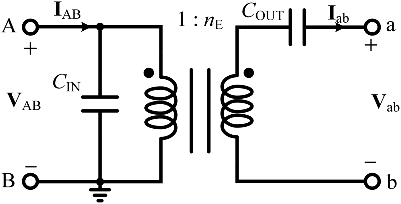
Based on (2) and (3), an equivalent circuit model of the capacitive-coupling interface can be established as illustrated in Fig. 5. This model includes three circuit components:
The proposed circuit model of the capacitive coupling.
The first one is an equivalent ideal transformer that couples the primary and secondary side, with a turns ratio n E:
 $$n_E = \displaystyle{{k_E C_2} \over {C_{ab} + C_2}}, $$
which is dependent on the alignment of coupling plates, indicating the coupling condition in some sense.
The second and third are the input capacitance C IN, and the output capacitance C OUT, which can be determined, respectively by:
 $$C_{IN} = C_{AB} + C_1 + \displaystyle{{C_{ab} C_2} \over {C_{ab} + C_2}} k_E^2, $$
 $$C_{OUT} = C_{ab} + C_2. $$
B) Effect of misalignment
According to (4), the ideal transformer is inherently a step-down transformer. It has a maximum turns ratio of 1:1 without cross-coupling. When cross-coupling is taken into consideration, the maximum turns ratio is C 2/(C ab + C 2). Besides, unlike conventional transformers always with a positive turns ratio, the turns ratio of the ideal transformer in the proposed model can be negative, which means that the direction of the coupled voltage on the secondary side is reversed (180° out of phase). In such a case, the cross-coupling has changed to such an extent that the cross capacitances (C Ba and C Ab) become larger than the designed main capacitances (C Aa and C Bb).
To provide a quantitative analysis of how misalignment affects the model, we define C C as the main capacitance between one single pair of plates (plates A and a or plates B and b) when they are aligned perfectly. Define α, β as the portion of plate coupled to plate B, and plate b coupled to plate A, respectively. So the cross-coupling capacitances C Ba = αC C, CAb = βC C. Assuming plates a and b are placed within the boundary of primary plates and the gap between plates A and B keeps constant, the main capacitances formed between plate A and plate a, plate B and plate b are C Aa = (1 − α)C C, CBb = (1 − β)C C. Thus, n E can be expressed as
 $$n_E = \displaystyle{{C_C} \over {2C_{ab} + C_C}} (1 - \alpha - \beta ).$$
Figure 6 shows the variation of normalized turns ratio n E with misalignment in the capacitive-coupling interface. At the condition of the best alignment, i.e. α = β = 0, the transformer has the maximum turns ratio. At the condition of the worst alignment, i.e. α + β = 1, the transformer has the minimum turns ratio, which is zero. When α = β = 1, it means plate A is completely coupled to plate b and plate B to plate a, which is equivalent to the condition in which α = β = 0, except for the reverse direction of the coupled voltage on the secondary side.
(a) Normalized turns ratio n E in relation to misalignment; (b) absolute value of the normalized turns ratio in relation to misalignment.
The input and output capacitances C IN and C OUT can also be expressed as
 $$C_{IN} = C_{AB} + (\alpha + \beta - \alpha ^2 - \beta ^2 )C_C + \displaystyle{{2C_{ab} C_C} \over {2C_{ab} + C_C}} (1 - \alpha - \beta )^2, $$
 $$C_{OUT} = C_{ab} + \displaystyle{{C_C} \over 2}.$$
In most practical CPT applications, capacitances C AB and C ab between plates on the same side are small compared with the main coupling capacitance C C. Ignoring C AB and C ab, nE, CIN, and C OUT can be expressed in terms of C C, α, and β, respectively:
 $$n_E = 1 - \alpha - \beta, $$
 $$C_{IN} = (\alpha + \beta - \alpha ^2 - \beta ^2 )C_C, $$
 $$C_{OUT} = \displaystyle{{C_C} \over 2}.$$
In Fig. 7, C IN/C C and C OUT/C C are plotted as the functions of misalignment ignoring C AB and C ab. Figure 7(a) shows that at the best alignment condition, input capacitance C IN will become zero. C IN reaches the maximum value at the worst coupling condition in which α = β = 0.5 when no power is coupled to the secondary side. Figure 7(b) shows that the output capacitance C OUT keeps a constant value of C C/2 regardless of variation of misalignment.
(a) Normalized input capacitance C IN/C C, and (b) normalized output capacitance C OUT/C C versus misalignment when C AB and C ab are ignored.
The three parameters in the proposed model interconnect with each other, describing the characteristics of the capacitive-coupling interface collectively. The ideal transformer in the model reflects the coupling condition between primary and secondary coupling plates. Unlike actual transformer, its turns ratio can never exceed unity, meaning that it is unity or step-down transformer inherently. Besides, it can become zero under the worst case of coupling. In the best coupling situation, the two pairs of coupling plates are well-aligned with each other without cross-coupling, yielding a unity of n E. For the worst case of coupling, the effect of cross-coupling cancels the main coupling capacitances, yielding a zero turns ratio, and no power can be transferred to the secondary side. Unlike the input capacitance C IN that varies with the alignment condition, the output capacitance C OUT keeps unchanged regardless of coupling conditions.
It should be noted that the analysis of the effect of misalignment on the model is based on the assumption that the distances between primary and secondary coupling plates keep unchanged. For those CPT systems in which the coupling distances change during operation, another varying factor can be introduced to take account of the coupling distance variation.
The three parameters of the proposed model can be determined easily by experiments. C IN can be measured at the input port A–B when the output port a–b is an open-circuit. C OUT can be measured at the port a–b when the input port A–B is shorted. The capacitive turns ratio n E can be obtained by applying an AC voltage at the input port A–B and measuring the ratio of the output open-circuit voltage to the input voltage.
The proposed model can provide a circuit-intuitive guideline for the selection of driving inverters and tuning circuits. It can be inferred that a voltage-fed inverter is not suitable for driving the capacitive-coupling interface directly since a capacitor C IN is at the input of the interface. Hence, a primary side series tuning inductor is always necessary when a voltage-fed inverter is used if less noise is required.
III. TUNING INDUCTOR ANALYSIS WITH PROPOSED MODEL
The proposed model is used for the calculation of a series tuning inductor and analysis of its tuning effect on CPT systems. The inductor can be placed in two different positions, either before the input capacitor C IN (referred to as primary side tuning), or after the output capacitor C OUT (referred to as secondary side tuning).
A) Primary side tuning
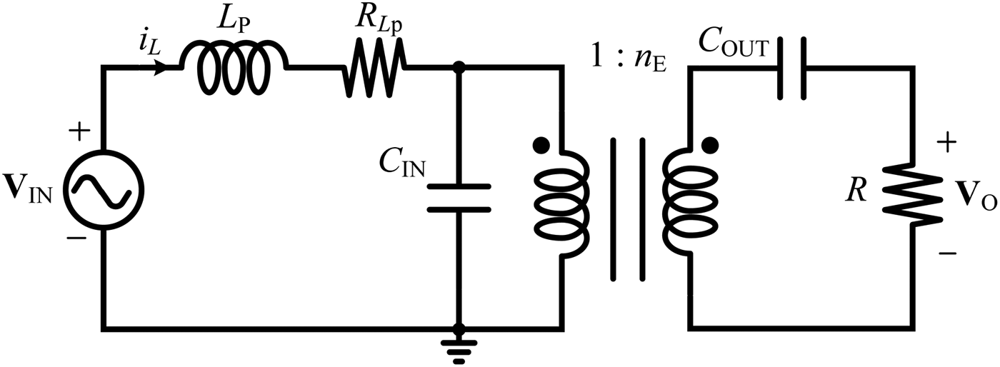
In Fig. 8, a tuning inductor L P with an equivalent series resistance R Lp is placed at the primary side to achieve full resonance. VIN is the input AC voltage source at an operating frequency of f S, R is the AC load or the equivalent resistance presented by the rectifier with a DC load.
Primary side tuning.
With the proposed model, the secondary side circuit can be reflected to the primary through the ideal transformer, as shown in Fig. 9. The CPT system is now reduced to a second order system. The current through the primary tuning inductor i L is:
 $${\bf I}_L = \displaystyle{{{\bf V}_{IN}} \over {j\omega L_P + R_{Lp} + (R_1 /1 + j\omega (C_{IN} + C_{OUT{\rm 1}} )R_1 )}},$$
where
 $$\omega = 2\pi f_S, $$
 $$C_{OUT{\rm 1}} = \displaystyle{{Q_S ^2} \over {1 + Q_S ^2}} n_E^2 C_{OUT}, $$
 $$R_1 = (1 + Q_S^2 )\displaystyle{R \over {n_E^2}}, $$
 $$Q_S = \displaystyle{1 \over {\omega C_{OUT} R}}.$$
Impedance transformation of primary side tuning.
The required tuning inductor L P can be calculated by setting imaginary part of IL to be zero:
 $$L_P = \displaystyle{1 \over {\omega ^2 (C_{IN} + C_{OUT{\rm 1}} )}}\displaystyle{{Q_1^2} \over {1 + Q_1^2}}, $$
where
 $$Q_1 = \omega R_1 (C_{IN} + C_{OUT{\rm 1}} ).$$
In terms of misalignment portion α and β, L P can be expressed as
 $$\eqalign{L_P = & \displaystyle{1 \over {\omega ^2 (C_C /2)}}\displaystyle{1 \over {2(\alpha + \beta - \alpha ^2 - \beta ^2 ) + (Q_S^2 /1 + Q_S^2 )(1 - \alpha - \beta )^2}} \cr & \times \displaystyle{{Q_1^2} \over {1 + Q_1^2}} \approx \displaystyle{1 \over {\omega ^2 (C_C /2)}}\displaystyle{1 \over {1 - (\alpha - \beta )^2}}.} $$
Figure 10 shows normalized primary tuning inductor L P/(1/(ω 2C C/2)) versus misalignment. It indicates that the value of the tuning inductance L P required to achieve resonance is affected by the difference between α and β. Thus, in the cases of symmetrical misalignment (α = β), L P keeps unchanged, which is equal to 1/(ω 2C C/2). Theoretically, if the absolute value of α–β equals 1, the inductance required to achieve resonance will become infinity.
Normalized primary side tuning inductance L P/(1/(ω 2CC/2)) versus misalignment.
The peak current through the tuning inductor i L is:
 $$i_{L,peak} = \displaystyle{{v_{IN{\rm,} peak}} \over {(R_1 /(1 + Q_1^2 )) + R_{Lp}}}, $$
where v IN, peak is the peak value of input AC voltage VIN.
It is noted that in practical applications, Q 1 should be small for accurately tuning the circuit since large Q 1 will make the system too sensitive.
Considering the losses of tuning inductor, P O1 is
 $$\eqalign{ P_{O{\rm 1}} &= \displaystyle{v_{IN, peak}^2 \over 2}\displaystyle{{1 + Q_1^2} \over {(R_1 + (1 + Q_1^2 )R_{Lp} )^2}} R_1 \cr & = \displaystyle{{v_{IN{\rm,} peak}^2} \over {2R}}\displaystyle{m \over {(1 + m\;(R_{Lp} /R))^2}},} $$
where
 $$m = \displaystyle{{n_E^2 (1 + Q_1^2 )} \over {1 + Q_S^2}}. $$
By (10)–(12), (15), (16), and (19), in terms of misalignment coefficient α and β, Q 1 can be expressed as
 $$Q_1 = \displaystyle{{\alpha + \beta - \alpha ^2 - \beta ^2} \over {(1 - \alpha - \beta )^2}} \left( {\displaystyle{2 \over {Q_S}} + 2Q_S} \right) + Q_S. $$
Assuming 100% efficiency, the output power P O1 received by the load R is
 $$P_{O{\rm 1}} = \displaystyle{{v_{IN{\rm,} peak}^2} \over {2R_1}} (1 + Q_1^2 ).$$
The output power using primary side tuning P O1 can be expressed as:
 $$P_{O{\rm 1}} = \displaystyle{{v_{IN{\rm,} peak}^2} \over {2R}}\displaystyle{{(1 - \alpha - \beta )^2} \over {1 + Q_S^2}} 1 + Q_1^2. $$
The term  $v_{IN{\rm,} peak}^2 /2R$ represents the nominal output power when the capacitive-coupling interface is fully compensated for by a series inductor in a CPT system without cross-coupling. Figure 11 shows the normalized output power P O1/(v 2IN, peak/(2R)) versus misalignment. The range of α and β is 0–0.4. The reason of choosing this range is that in practical CPT applications misalignment will be controlled to avoid extreme misalignment that causes very little or no power. The maximum output power after adding tuning inductor increases with misalignment. Although theoretically, the power will become very large when α and β are close to 0.5, the output power of practical systems cannot go to arbitrarily high since the current through the tuning inductor will become quite large leading to significant losses. Figure 12 shows the normalized output power P O1/(v 2IN, peak/(2R)) versus misalignment including the losses of the tuning inductor when R Lp/R = 0.2. When the inductor losses are taken into account, the output power increases at first and then drops with significant misalignment due to the increased inductor losses. The output power reaches the maximum at a certain configuration of misalignment. Thus, it is concluded that a reasonable small misalignment can help to increase output power.
Normalized output power P O1/(v 2IN, peak/(2R)) versus misalignment when R Lp/R = 0.
Normalized output power P O1/(v 2IN, peak/(2R)) versus misalignment when R Lp/R = 0.2, (a) 0 < α, β < 0.4, (b) 0 < α, β < 1.
B) Secondary side tuning
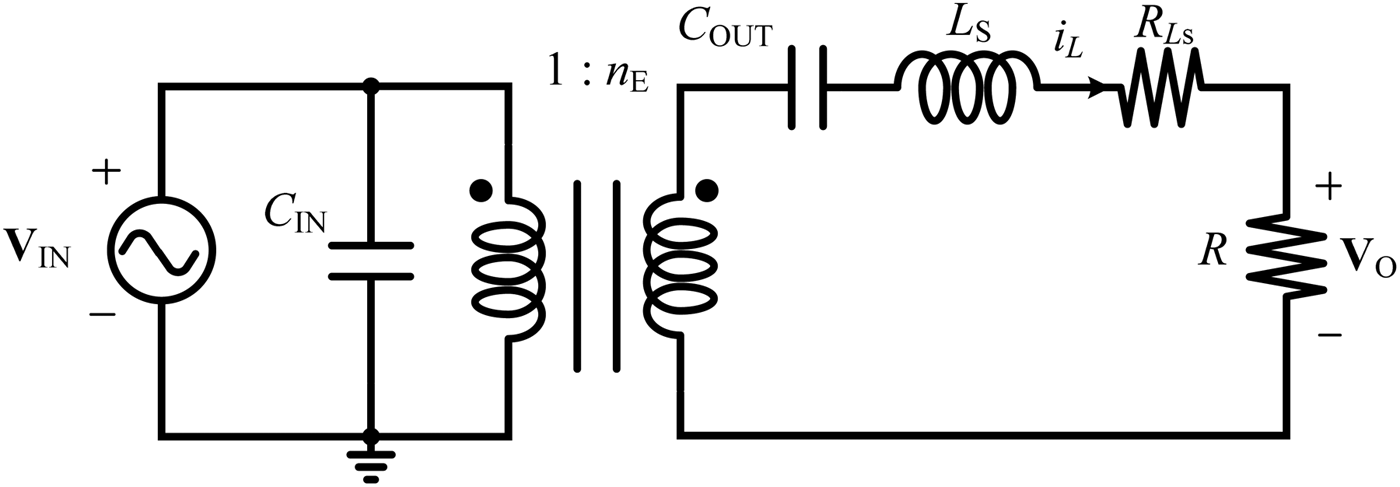
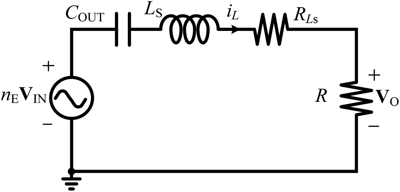
Figure 13 shows the situation where the tuning inductor is placed on the secondary side of a CPT system. Similarly, the CPT system with secondary side tuning inductor can be simplified in Fig. 14. Different from the primary side tuning, the secondary side inductor is used to compensate for the output capacitance C OUT. To achieve the maximum power transfer, the secondary side tuning inductor L S can be calculated by
 $$L_S = \displaystyle{1 \over {\omega ^2 C_{OUT}}}. $$
Secondary side tuning.
Impedance transformation of secondary side tuning.
The peak current through L S is
 $$i_{L,peak} = \displaystyle{{n_E v_{IN{\rm,} peak}} \over {R_{Ls} + R}}.$$
Considering the losses of tuning inductor, P O2 is
 $$P_{O{\rm 2}} = \displaystyle{{(n_E v_{IN{\rm,} peak} )^2} \over 2}\displaystyle{R \over {(R_{Ls} + R)^2}}. $$
Assuming 100% efficiency, the power P O2 received by the load R is
 $$P_{O{\rm 2}} = \displaystyle{{(n_E v_{IN{\rm,} peak} )^2} \over {2R}}.$$
C) Comparison of output power
The output power using secondary side tuning P O2 can be expressed as
 $$P_{O{\rm 2}} = \displaystyle{{v_{IN{\rm,} peak}^2} \over {2R}}(1 - \alpha - \beta )^2. $$
According to (26) and (31), the ratio between the output power with primary and secondary tuning inductors is defined by γ, which is
 $$\gamma = \displaystyle{{P_{O{\rm 1}}} \over {P_{O{\rm 2}}}} = \displaystyle{{1 + Q_1^2} \over {1 + Q_S^2}}. $$
From (15), (16), and (19), Q 1 can be expressed in terms of Q S:
 $$Q_1 = \displaystyle{{\omega C_{IN} R} \over {n_E^2}} (1 + Q_S^2 ) + Q_S. $$
From (33), Q 1 equals Q S when no misalignment exists between plates making C IN zero. Otherwise, Q 1 is greater than Q S, since γ is >1. Hence, it is preferred that the series tuning inductor is placed on the primary side if more power is desired.
Figure 8 shows that the primary side tuning inductor and the input capacitance form a parallel tank which helps to boost the input voltage, producing more power. Note that in the secondary side compensation in Fig. 13, the tuning inductor and output capacitance form a series resonant tank. The output voltage would therefore be lower than the input voltage considering n E is <1. Furthermore, the secondary side tuning is not desirable if a voltage-fed converter is used since the parallel capacitor C IN will be connected directly with the primary voltage source, generating significant current spikes.
IV. SIMULATIONS AND EXPERIMENTAL RESULTS
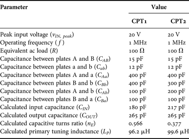
To verify the proposed model in determining the accurate tuning inductances, a prototype CPT system are constructed with four coupling plates intentionally misaligned as shown in Fig. 15. Two cases of different misalignment are investigated, referred to as CPT1(α = β = 0.2) and CPT2 (α = 0.2, β = 0.4). The practical capacitive-coupling interface of the prototype CPT system includes two 150 × 300 mm aluminium sheets and two 50 × 100 mm copper pads (capacitance of one pair of plates C C = 500 pF), which are all coated with a thin layer of polypropylene as dielectric material, and is driven by a 1 MHz sinusoidal voltage source from a power amplifier. Two terminal cross-coupling capacitances (C AB and C ab) are measured with a precision RLC meter (Agilent 4980) when primary and secondary plates are decoupled. Four coupling capacitances (C Aa, CBa, CAb, and C Bb) are calculated based on variations of overlapping area between the coupling plates. The parameters of the system are listed in Table 1. Both systems use primary side tuning inductors calculated based on proposed model.
The Prototype CPT system.
CPT system specification.
A) Misalignment variation
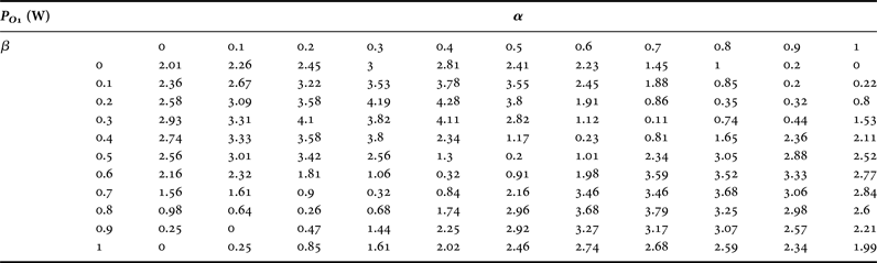
Figures 16 and 17 show simulated and experimental results, which demonstrate that voltage v AB and current i L into the resonant circuit are in phase. The actual values of the inductor in the experiments are 92 and 94 µH, which are slightly smaller than calculated. The parasitics in the circuits contribute some inductance. It also shows that the current is less than the simulated value due to the conduction and core losses of the tuning inductor at high frequency operation. The difference between the experimental and simulated waveforms will be reduced if the inductor is optimized for high frequency operation (using better ferrites and litz wires suitable for high frequency). The output powers of CPT1 and CPT2 are measured to be 3.48 and 3.58 W, respectively. The output power of CPT2 is slightly larger than CPT1 because the misalignment of CPT2 is larger than that of CPT1, which agrees with the prediction from the model. Figure 18 shows the output power as a function of a full range of variation of misalignment, which is in agreement with Fig. 12(b) derived from the model except for some extreme conditions. With severe misalignment the inductor current becomes very large at resonance that will lead to significant losses, so the output power cannot maintain high output power at the vicinity of points where α = 0, β = 1 and α = 1, β = 0 (Table A1).
Experimental simulated data plots of input voltage v IN and input current i L of CPT1.
Experimental simulated data plots of input voltage v IN and input current i L of CPT2.
Experimental data plots of the normalized output power P O1/(v 2IN, peak/(2R)) versus misalignment (v 2IN, peak/(2R) = 2 W).
B) Load variation
In order to evaluate the effect of load variation on the output power, the load of CPT2 system is varied since it can produce more power. Figure 19 shows the output power variations with the load. It shows that the measured values are in good agreement with calculated values based on the proposed model. At light load, the deviation of the model from the experimental results increases because the larger load resistance yields lower tank quality.
Output power versus load R.
V. CONCLUSION
This paper presents an accurate steady-state model of the capacitive-coupling interface of CPT systems with cross-coupling. Effects of misalignment on parameters of the proposed model are analyzed in detail. It shows that the input capacitance and the ideal transformer of the model vary with different coupling conditions, while the output capacitance keeps constant. The developed model was applied to determine the series tuning inductances of a CPT system with cross-coupling on primary and secondary side to achieve full resonance, and the effect of misalignment on the output power was analyzed. Simulations and experimental results have verified the effectiveness of the proposed model. The results of both simulations and experiments show that the calculated primary side tuning inductance can be used to achieve full resonance. It has demonstrated that misalignment within reasonable range can increase output power at resonance and the measured output power versus misalignment and load changes agrees well with the results predicted by the model.
ACKNOWLEDGEMENTS
We would like to show our gratitude to Howard Lu for helping built the experimental setup.
APPENDIX
Experimental data for Fig. 18.
Liang Huang received his B.Sc. degree in Electrical Engineering from Huazhong University of Science and Technology, Wuhan, China, in 2008 and received his M.E. degree in Mechatronic Engineering from Chongqing University, Chongqing, China, in 2011. He is presently pursuing the Ph.D. degree in Power Electronics at The University of Auckland, Auckland, New Zealand. His main research interests are the field of power electronics, including the design and optimization of high frequency converters, wireless power transfer, and capacitive power transfer.
Aiguo Patrick Hu graduated from Xian JiaoTong University, China, with B.E. and M.E. degrees in 1985 and 1988, respectively. He received his Ph.D. degree from the University of Auckland in 2001 before he worked as a Lecturer, Director of China–Italy Cooperative Technical Training Centre in Xian, and the General Manager of a technical development company. He holds more than 10 patents in wireless/contactless power transfer and microcomputer control technology, published more than 130 referred journal and conference papers, authored the first monograph on wireless inductive power transfer technology, and contributed four book chapters on inductive power transfer modeling/control and electrical machines. Dr. Patrick is now with the Department of Electrical and Computer Engineering, The University of Auckland, New Zealand, and also a Guest Professor of Chongqing University. His research interests include wireless/contactless power transfer technologies and application of power electronics in renewable energy systems.
 Akshya K. Swain received his B.Sc. degree in Electrical Engineering and the M.Sc. degree in Electronic Systems and Communication from Sambalpur University, Sambalpur, India, in 1985 and 1988, respectively, and the Ph.D. degree from the Department of Automatic Control and Systems Engineering, University of Sheffield, Sheffield, UK, in 1997. From 1994 to 1996, he was a Commonwealth Scholar in the UK. Since September 2002, he has been with the Department of Electrical and Computer Engineering, The University of Auckland, Auckland, New Zealand. His present research interests include nonlinear system identification and control, biomedical signal processing, sensor networks, and control applications to power system and wireless power transfer systems. Dr. Swain is an Associate Editor of IEEE Sensors Journal and Member of the Editorial Board of International Journal of Automation and Control and International Journal of Sensors, Wireless Communications, and Control.
Yu-Gang Su (M'09) received his B.E. and M.E. degrees in Industry Automation, and the Ph.D. degree in Control Theory and Control Engineering from Chongqing University, Chongqing, China, in 1985, 1993, and 2004, respectively. From 2008 to 2009, he was a Visiting Scholar at the University of Queensland, Brisbane, Australia. He is presently a Professor at the College of Automation, Chongqing University. His research interests include power electronics, control theory and applications, wireless power transfer.