I. INTRODUCTION
Cu is an important material used in many fields such as electrical engineering and electronics. It is characterized by low electrical resistivity, high thermal conductivity, and good resistance to stress voiding and electromigration. Reference Huang, Lai, Tsai, Huang, Lin and Lee1,Reference Gupta, Wang, Kvit, Duscher and Narayan2 However, due to its low hardness (∼0.65 GPa for bulk Cu) Reference Yao, Han, Li, Tao and Lu3 and easy reactions with surrounding dielectrics such as Si, SiO2, etc., Reference Zhou, Gustafsson and Garfunkel4–Reference Li, Liu, Zhang, Chu, Wang and Dong6 pure Cu cannot be directly used in applications requiring high hardness and chemical inertness. Therefore, it is essential to explore a simple and effective way to solve these problems. Generally, the hardness improvement of Cu can be achieved through two methods, i.e., surface treatment and matrix alloying. However, the overall conductivity inevitably decreases with the direct introduction of alloying elements into the Cu matrix. Reference Batra, Dey, Kulkarni and Banerjee7 Thus, the surface treatment of Cu is a good choice to keep the good matrix electrical conductivity, and increase the hardness and chemical inertness as well.
For the surface nitriding treatment, high temperature gas nitriding and low temperature plasma nitriding are the two common methods. Cu is generally considered as an unsuitable nitrided material because the decomposition temperature of the Cu–N compound (Cu3N) is in the range of 100–470 °C. Reference Wang, Nakamine and Hayashi8–Reference Nosaka, Yoshitake, Okamoto, Ogawa and Nakayama12 Even in the conventional low temperature nitriding process, it (480–550 °C) is also higher than that. If the nitriding of Cu is realized by reducing temperature, the nitride layer will become shallower, the nitriding period will be very long, and the problem of decomposition of Cu–N compounds will still not be solved essentially.
In addition to nitriding, coating is also used to improve the surface hardness of Cu, such as Cu–Al2O3 dispersion strengthened layer with high hardness and wearability prepared by sintering on the Cu or Cu alloy surface. Reference Li, Sun, Yan, Liu, Wang and Luo13 Cabrera et al. Reference Cabrera, Kirner and Armor14 siliconized Cu surface to obtain copper-silicon solid solutions or compounds, thereby significantly improving the wear resistance of the surfaces. While aluminizing and titanizing brass obtained the excellent corrosion resistance, wear resistance, and oxidation resistance. Although these coatings can improve the surface strength of Cu, the high performed temperatures (∼1000 °C) will easily lead to the oxidation or phase transformation of the matrix, thus affecting its properties. Moreover, the thickness of coating is generally greater, holes and other defects (e.g., segregation) are easily formed in the hardened layer or at the interface.
In this paper, we attempt to prepare the CuN-based alloy films to improve the hardness and maintain good matrix electrical conductivity, which is expected to displace some heterogeneous coatings of Cu. However, the key issue is how to stabilize N in the Cu film. So a suitable alloying element is needed. According to the table of mixing enthalpies Reference Takeuchi and Inoue15 : ΔH N–Cu = −84 kJ/mol, ΔH Cu–Cr = 12 kJ/mol, ΔH N–Cr = −107 kJ/mol, ΔH Cu–Zr = −23 kJ/mol, ΔH N–Zr = −233 kJ/mol. The great and negative ΔH N–Cr and ΔH N–Zr means that Cr and Zr can easily combine with N to form hard stable nitrides. Furthermore, the transition-metal nitride electrical conductor thin films, thank to extremely low vacancy mobilities, Reference Sangiovanni, Alling, Steneteg, Hultman and Abrikosov16 are typically used to prevent Cu from diffusing, Reference Mühlbacher, Bochkarev, Mendez-Martin, Sartory, Chitu, Popov, Puschnig, Spitaler, Ding, Schalk, Lu, Hultman and Mitterer17 thus preserving the device electronic properties while maintaining electrical contact. Therefore, the transition-metal nitride in Cu films might be beneficial to prevent diffusion of Cu, that is, it can increase the chemical inertness of Cu.
Thus, the Cu(Cr, N) and Cu(Zr, N) ternary alloy films will be prepared by magnetron sputtering on the single crystal Si(100) substrates and analyzed composition, micro-structure, hardness, and resistivity for high hardness nitrogenous Cu alloy films and exploring the influences of different N stabilizing elements on film properties.
II. EXPERIMENTAL PROCEDURE
The Cu(Cr, N) and Cu(Zr, N) ternary films were prepared by RF magnetron sputtering method. Si(100) wafer with native oxide layer (about 3∼5 nm) was used as the substrate. The sputtering target consisted of Cu (purity: 99.999 wt%, diameter: 75 mm) and Cr (99.95 wt%) or Zr (99.9 wt%) slices were embedded in its main sputtering zone. The chamber was pumped with a rotary pump down to 5 Pa and then was vacuumed to 8.0 × 10⁻⁴ Pa using molecular pump. Then the N2/Ar ratio (1/15, 1/10, 1/5) were adjusted to obtain different film composition. Meanwhile, pure Cu, and Cu(N) films were prepared as reference. The working pressure was 0.4 Pa, using sputtering power 100 W and substrate–target distance 10 cm. Vacuum annealing processes were performed for 1 h at temperatures ranging from 200 to 550 °C. The samples transferred from the deposition chamber to the analysis chambers were carried out under the air condition, so the surface of the films might be oxidized lightly.
The micro-zone composition and depth composition profiles of the films were measured with Electron-probe Micro-Analyzer (EPMA-1600; Shimadzu Corp., Kyoto, Japan) and Auger Electron Spectroscopy (AES; PHI-700, ULVAC-PHI Inc., Chigasaki, Japan), respectively. Chemical states of elements in the films were characterized using X-ray photoelectron spectroscopy (XPS; ESCALAB 250Xi, Thermo Fisher Scientific, Waltham, Massachusetts). The adventitious C1s peak at 284.8 eV was used to calibrate the binding energy scale. Structural studies of the films were carried out by grazing-angle incidence X-ray diffraction (XRD) with a grazing angle of 1° (Cu Kα, out-of-plane mode) and transmission electron microscopy (TEM; Philips Tecnai G2, FEI Company, Amsterdam, The Netherlands). Step tester (ET4000M, Kosaka Laboratory Ltd., Kosaka, Japan) was used to measure the thicknesses. The resistivities of films were measured through the four-point probe method. And the hardness of films was carried out from Micro-nano durometer (FISCHERSCOPE HM2000, Helmut Fischer GmbH, Sindelfingen, Germany), with the maximum expected load of 15 mN, the maximum indentation depth of about 350 nm and the loading duration of 20 s.
III. RESULTS AND DISCUSSION
A. Film composition analysis
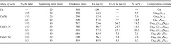
Table I shows the preparation processes, thicknesses, and composition of the as-deposited Cu, Cu(N), Cu(Cr, N), and Cu(Zr, N) films. With the increase of N2/Ar ratio (or increase of N2 partial pressure), the content of N in the Cu(N) films increased from 5.5 to 12.5 at.%. However, for the Cu (Cr, N) films, Cr content decreased from 26.2 to 22.1 at.% and N content increased from 18.2 to 20.6 at.%. That can be explained as the increase of N2 partial pressure caused the relatively decrease in the number of Ar+ bombarding the target. As a result, sputtering rate reduces accordingly and the film thickness gradually decreases.
Preparation processes, thicknesses and composition of the as-deposited Cu, Cu (N), Cu(Cr, N) and Cu(Zr, N) films.

Compared with Cu(Cr, N) film, the total alloying elements content of the Cu(Zr, N) film under the same sputtering process (N2/Ar ratio, power, time, and area of slices) is lower, due to the sputtering yield of Zr is lower than Cr Reference Laegreid and Wehner18 (the atomic size of Zr is larger than Cr). As N2/Ar ratio increased, Zr content was gradually decreased from 7.5 to 4.9 at%. But the N content is independent from N2/Ar ratio, showing the maximum value (7.8 at.%) at the N2/Ar ratio of 1/10.
Figure 1 shows the AES depth profiles of the as-deposited Cu57.3Cr22.1N20.6 and Cu88.8Zr4.9N6.3 films. It can be observed that Cr (or Zr) and N is homogeneously distributed in the depth direction. The Cr (or Zr) concentration is approximately equal to N concentration. Therefore, the results of composition analysis indicate that the N concentration is related to the amount of suitable elements (Cr or Zr).
AES depth profiles of the as-deposited Cu57.3Cr22.1N20.6 (a) and Cu88.8Zr4.9N6.3 (b) films.

B. Film chemical state analysis
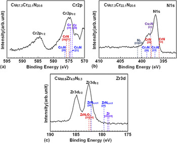
Figures 2(a) and 2(b) present the Cr2p and N1s XPS spectra for as-deposited Cu57.3Cr22.1N20.6 film, respectively. As shown in Fig. 2(a), the dotted lines indicate the position of Cr2p 3/2 peaks under the different chemical configurations of Cr reported in literature. Reference Moulder, Stickle, Sobol and Bomben19–Reference Kong, Ji, Li, Liu and Wang21 In the case of the Cr2p 3/2 component, the binding energies for pure Cr are 574 eV Reference Conde, Cristóbal, Fuentes, Tate and de Damborenea20 and 574.5 eV Reference Moulder, Stickle, Sobol and Bomben19 , for CrN are 575 eV Reference Conde, Cristóbal, Fuentes, Tate and de Damborenea20 and 575.8 eV Reference Kong, Ji, Li, Liu and Wang21 , for Cr2N are 574.8 eV Reference Kong, Ji, Li, Liu and Wang21 and 576.4 eV Reference Conde, Cristóbal, Fuentes, Tate and de Damborenea20 , respectively. Distinctly, the reference values for the Cr2p 3/2 binding energy in the Cr, CrN, and Cr2N showed small shifts. Therefore, the type of chromium compounds cannot be determined just according to the peak of Fig. 2(a). From Fig. 2(b), the XPS spectrum of N1s deviates from the N1s binding energy in adsorbing N2 (400.2–401 eV Reference Rizzo, Signore, Mirenghi and Dimaio22 ). The associations between N1s peaks positions and compounds are as followed: 396 and 397.8 eV to CrN, Reference Conde, Cristóbal, Fuentes, Tate and de Damborenea20–Reference Lavigne, Alemany-Dumont, Normand, Berthon-Fabry and Metkemeijeret23 397 and 398.8 eV to Cr2N, Reference Conde, Cristóbal, Fuentes, Tate and de Damborenea20–Reference Lavigne, Alemany-Dumont, Normand, Berthon-Fabry and Metkemeijeret23 ∼398 eV to Cu–N. Reference Cui, Lane, Vijayamohanan and Ramanath24 Apparently, the N1s peak is located between the references positions of Cr2N and CrN. Therefore, combined with the analysis of N1s peak, Cr2N or CrN is existed in the films, which need to be further analyzed.
XPS spectra for the as-deposited films: (a) Cr2p, (b) N1s (obtained from the Cu57.3Cr22.1N20.6 film), (c) Zr3d (obtained from the Cu88.8Zr4.9N6.3 film). The dotted lines indicate the position of Cr2p 3/2, Zr3d 5/2 and N1s peaks under the different chemical configurations of Cr, Zr and N reported in XPS handbook and literature, respectively.

Figure 2(c) shows the Zr3d XPS spectrum for as-deposited Cu88.8Zr4.9N6.3 film, the dotted lines indicate the position of Zr3d 5/2 peaks under the different chemical configurations of Zr reported in literature. Reference Moulder, Stickle, Sobol and Bomben19,Reference Rizzo, Signore, Mirenghi and Dimaio22,Reference Cheng and Zheng25,Reference Roman, Bernardi, de Amorim, de Souza, Spinelli, Giacomelli, Figueroa, R Baumvol and Basso26 The Zr3d 5/2 binding energy peaks corresponding to pure Zr are 178.7 and 178.9 eV. Reference Moulder, Stickle, Sobol and Bomben19 Zr–N compounds (ZrN x , x ≤ 1) are in the majority, the reference Zr3d 5/2 binding energies for ZrN x are 179.6 eV and 182.1 eV, Reference Cheng and Zheng25,Reference Roman, Bernardi, de Amorim, de Souza, Spinelli, Giacomelli, Figueroa, R Baumvol and Basso26 for ZrN x O y are 182.2 eV and 182.5 eV, Reference Cheng and Zheng25 respectively. Therefore, the position of Zr3d 5/2 peak shows that the nitrides of Zr and the nitrogen oxides of Zr may exist in the film. The content of light element N is less in the films (∼6.3 at.%), however, the intensity of N1s peak is very low, it is not suitable for further confirmation of the existing form of Zr and N.
C. Film microstructure analysis
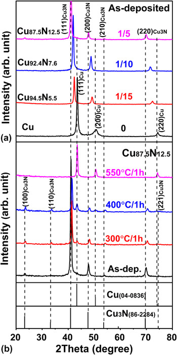
Figure 3 shows the XRD patterns of the as-deposited Cu, Cu(N) films and the Cu87.51N12.5 film after annealing at different temperatures for 1 h. The Cu peaks gradually transform into the Cu3N peaks with the increase of N2/Ar ratio, as shown in Fig. 3(a). However, as the increase of the annealing temperature, the Cu3N in Cu87.51N12.5 film gradually decompose and the Cu peaks reappear [Fig. 3(b)]. After annealing at 550 °C for 1 h, the Cu3N peaks disappear, indicating the Cu3N have been completely decomposed. It also confirms that Cu3N could not exist above the decomposition temperature of 470 °C. Reference Wang, Nakamine and Hayashi8−Reference Nosaka, Yoshitake, Okamoto, Ogawa and Nakayama12
XRD patterns of the as-deposited Cu and Cu(N) films (a) as well as the Cu87.51N12.5 film after annealing at different temperatures for 1 h (b).

The low and broad Cu peaks appears in the patterns of the as-deposited Cu(Cr, N) films [Fig. 4(a)], which is the characteristic of nanocrystalline. As the N2/Ar ratio increases to 1/5, a weak broad diffraction peak appears on the left of Cu peak in the Cu57.3Cr22.1N20.6 film. The standard diffraction peaks of Cr2N (JCPDS file no. 35-0803) and CrN (JCPDS file no. 77-0047) are closed to this position, showing the Cr2N or CrN crystallization phase begins to appear. As the raise of the annealing temperature, the crystallization of Cu57.3Cr22.1N20.6 film is improved [Fig. 4(b)], and the diffraction intensity of Cu and Cr–N compounds peaks increase. Furthermore, the diffraction peaks of Cr–N compound still existed in the 550 °C/1 h-annealed film, the temperature is higher than the decomposition temperature of Cu3N annealing, indicating Cr enable N to stably exist in the Cu films.
XRD patterns of the as-deposited Cu(Cr, N) films (a) and the Cu57.3Cr22.1N20.6 film after annealing at different temperatures for 1 h (b).

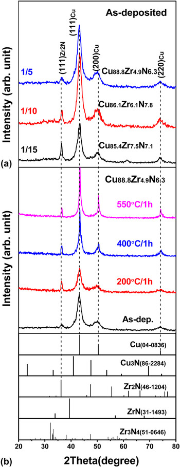
However, the Cu(Zr, N) films are crystallized to a great extent according to Fig. 5(a), the Zr2N peak (JCPDS file no. 46-1204) appears in the patterns, indicating the presence of Zr–N compounds in the film. Likewise, as the raise of the annealing temperature [Fig. 5(b)], the crystallinity of Cu88.8Zr4.9N6.3 film raises, and Zr2N diffraction peaks still existed in the 550°C/1 h-annealed film, indicating Zr also enable N to stably exist in the Cu films.
XRD patterns of the as-deposited Cu(Zr, N) films (a) and the Cu88.8Zr4.9N6.3 film after annealing at different temperatures for 1 h (b).

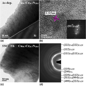
To further verify the microstructures of the Cu–N based films, two typical amorphous films (Cu56.7Cr24.7N18.6 and Cu86.1Zr6.1N7.8) were selected for TEM observations. The cross-sectional morphology of the as-deposited Cu56.7Cr24.7N18.6 film is shown in Fig. 6(a). It can be clearly observed that the film/substrate interface is clear and the film is composed of nano-scale particles. For the small particles, an analysis of a high-resolution TEM (HRTEM) image was performed [Fig. 6(b)]. The corresponding Fourier transform spectrum (in the right corner) shows that the small particle is Cr2N and that is the type of Cr–N compound in the Cu(Cr, N) films. The cross-sectional TEM morphology [Fig. 6(c)] and selected area electron diffraction (SAED) pattern [Fig. 6(d)] of the Cu56.7Cr24.7N18.6 after annealing at 550 °C for 1 h do not change significantly, suggesting that the structure of the film is relatively stable.
Cross-sectional TEM morphology of the as-deposited (a) and 550 °C/1 h-annealed (c) film Cu56.7Cr24.7N18.6. HRTEM image of crystallization particles in the as-deposited film (the corresponding Fourier transform spectrum in the right corner) (b). SAED pattern of the 550 °C/1 h-annealed film (d).

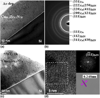
Likewise, the as-deposited Cu86.1Zr6.1N7.8 film [Fig. 7(a)] is also uniform, and the interface is quite smooth. The SAED pattern [Fig. 7(b)] shows sharp and continuous rings, indicating that the film is composed of Cu and Zr2N nanocrystals. After annealing at 550 °C for 1 h, the film/substrate interface is still clear and smooth, and it is still composed of nanocrystals. As shown in Fig. 7(d), the corresponding Fourier transform spectrum (in the upper right corner) and the filtering image (in the bottom right corner) of high-resolution TEM image show that the small particle is Zr2N, indicating the Zr2N nanocrystals exist stability.
Cross-sectional TEM morphology of the as deposited (a) and 550 °C/1 h-annealed (c) film Cu86.1Zr6.1N7.8. SAED pattern of the as-deposited film (b). HRTEM image taken inside the 550 °C/1 h-annealed film [the corresponding Fourier transform spectrum (in the upper right corner) and filtering image (in the bottom right corner)] (d).

From the view point of mixing enthalpy, the enthalpies of mixing between N and Cr (or Zr) are ΔH N–Cr = −107 kJ/mol and ΔH N–Zr = −233 kJ/mol, respectively, which are more negative than the ΔH N–Cu = −84 kJ/mol. Reference Takeuchi and Inoue15 Therefore, the N in the film will combine with Cr or Zr firstly and generate Cr2N or Zr2N. Thus, the formation probability of Cu3N will be reduced. Furthermore, the thermal decomposition temperatures of Cr2N and Zr2N are significantly higher than that of Cu3N (100–470 °C). Reference Wang, Nakamine and Hayashi8−Reference Nosaka, Yoshitake, Okamoto, Ogawa and Nakayama12 So the thermal stability of the ternary film comes from the strong interaction between Cr (or Zr) and N which is contributing to the generation of stable nitrides. The decomposition temperature of Cu3N is low which will cause the film loose and then make diffusion easily. So the stability of the film cannot remain.
In addition, it should be mentioned that, as the temperature rises to 550 °C, all films are free of reaction between Cu film and substrate Si according to the XRD or TEM analysis. In Refs. Reference Zhou, Gustafsson and Garfunkel4,Reference Chu, Lin and John5 Cu suffers from detrimental reactions with Si and SiO2 even at low temperatures near 200 °C, and for the Cu/Si structure, Reference Li, Liu, Zhang, Chu, Wang and Dong6 Cu3Si massively formed in the interface after annealing at 400 °C for 1 h. Therefore, the addition of Cr–N and Zr–N can increase the chemical inertness of Cu film.
D. Film properties analysis
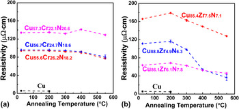
Figure 8 shows the resistivity evolution of the Cu, Cu(Cr, N) (a), and Cu(Zr, N) (b) films as functions of annealing temperature. However, the resistivity of pure Cu film does not show above 200 °C, because pure Cu can easily react with Si at low temperatures (near 200 °C), Reference Zhou, Gustafsson and Garfunkel4,Reference Chu, Lin and John5 resulting in a sharp decline of stability and Cu/Si structure break up. The resistivity of the Cu(Cr, N) and Cu(Zr, N) films is much higher than that of pure Cu film, mainly due to the Cr–N and Zr–N addition. As the annealing temperature rises, the resistivity of all ternary films [especially the Cu(Zr, N) films] drops down mainly because of the larger crystallinity, release of stress, the elimination of defect, out-diffusion of the residual N etc. However, it is still higher than that of pure Cu film due to the Cr2N and Zr2N exist stability.
Resistivity evolution of the Cu, Cu(Cr, N) (a) and Cu(Zr, N) (b) films as functions of annealing temperature.

Table II shows the hardness measurement results of the as-deposited and 400 °C/1 h-annealed Cu(Cr, N) (a) and Cu(Zr, N) (b) films. Obviously, the hardness of Cu(Cr, N) and Cu(Zr, N) films is higher than that of bulk Cu (0.65 GPa), showing the high hardness Cu alloy films using Cr or Zr for stabilizing N can be successfully gained. The hardness of the as-deposited Cu(Cr, N) films ranges from 4.5 to 6.5 GPa, however, for the Cu(Zr, N) films, it ranges from 4.1 to 4.7 GPa. Moreover, the effect of annealing temperature on the hardness of films is negligible. After annealing at 400 °C for 1 h, the hardness of Cu57.3Cr22.1N20.6 and Cu88.8Zr4.9N6.3 films are still up to 6.3 and 4.4 GPa, which is only a slight decrease compared to as-deposited film due to the release of stress, the elimination of defect, out-diffusion of the residual N etc.
Hardness values in GPa of the as-deposited and 400 °C/1 h-annealed Cu(Cr, N) and Cu(Zr, N) films.

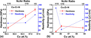
Deservedly, the applications of thin film should consider the increase of hardness as well as the smallest change of resistivity. Therefore, Fig. 9 comprehensively displays the hardness and resistivity of the as-deposited ternary films as a function of Cu content and the N2/Ar ratio. As shown in Fig. 9(a), the hardness and resistivity of Cu(Cr, N) films rise monotonously with the N2/Ar ratio and the increasing of Cu content. However, as the N2/Ar ratio equals 1/10, Cu(Cr, N) film displays a relatively high hardness and a relatively low resistivity.
Hardness and resistivity of the as-deposited Cu(Cr, N) (a) and Cu(Zr, N) (b) films as a function of Cu content and the N2/Ar ratio.

Compared with Cu(Cr, N) film, the addition of Zr–N into Cu film has a greater impact on the resistivity [Fig. 9(b)]. So Cu(Zr, N) film with relatively low total alloying elements content has relatively high resistivity, especially the as-deposited Cu85.4Zr7.5N7.1 film which reaches 165.9 μΩ·cm. Meanwhile, the resistivity and hardness are not monotone changing with the N2/Ar ratio and Cu content increasing, it decreases at first and then increases, the minimum resistivity and maximum presents in the N-maximum film (Cu86.1Zr6.1N7.8) which is also prepared at the N2/Ar ratio of 1/10.
The reason that the N2/Ar ratio of 1/10 as the best proportion because Cu(Cr, N) and Cu(Zr, N) films are composed of nanocrystals (Cu and Cr2N, Cu and Zr2N nanocrystals), and the residual N might be dissolved into CuN solid solutions. Therefore, the source of the high hardness includes grain refining, precipitation or solid solution strengthening. Inevitably, the resistivity would also be affected collectively by these three kinds of reinforcement sources.
In Fig. 9, the hardness and resistivity of Cu–Cr–N and Cu–Zr–N films has different variation tendencies versus the composition and N2/Ar ratios, which obviously associates with the N content in the films. The structural analysis shows that the N exists in the film in two states, precipitation state (Cr2N/Zr2N) and solid solution state (a small amount of solid solution N in Cu lattice). Both of these two states can increase the film hardness (strengthen), but for the influence of the resistivity is complex: in the Cu–Cr–N films (contenting 55–58 at.% Cu), the content of N and the resistivity increase monotonically with the increase of N2/Ar ratio. There are more Cr2N precipitations in this system, which is equivalent to purify the Cu matrix. However, the surplus of N in the form of solid solution increase resistivity at the same time, the precipitated phase also increases the scattering and then increases the resistivity. For the Cu–Zr–N film (contenting 85–89 at.% Cu), the N content is low at a N2/Ar ratio of 1/15, increases to a maximum value at 1/10, and then decreases again at 1/5. The resistivity shows an opposite tendency, indicating the N in the form of precipitation displays more obvious purification effect on the matrix and larger influence on resistivity.
In addition, grain refining also will strengthen alloys and increase the resistivity at the same time. However, both series of films are nanocrystals, as the N2/Ar ratio increase, the change of the grain size is not obvious, which displays less influence on the resistivity change trend.
IV. CONCLUSIONS
The high hardness CuN-based alloy films using Cr or Zr for stabilizing N were successfully prepared on single crystal Si(100) substrates by magnetron sputtering. The N content of films is related to the amount of alloying elements (Cr or Zr). Cu(Cr, N) films are composed of Cu and Cr2N nanocrystals and Cu(Zr, N) films are composed of Cu and Zr2N nanocrystals. The source of the high hardness includes grain refining, precipitation, or solid solution strengthening. From the perspective of resistivity and hardness, the Cu(Cr, N) and Cu(Zr, N) films prepared at the N2/Ar ratio of 1/10 show the relatively preferable properties. The hardness and resistivity of Cu56.7Cr24.7N18.6 film is 5.8 GPa and 96.1 μΩ·cm, whereas for the Cu86.1Zr6.1N7.8 film is 4.7 GPa and 63.6 μΩ·cm. The chemical inertness of Cu film can also be improved by adding Cr–N and Zr–N. These Cu(Cr, N) and Cu(Zr, N) films with high hardness and stable properties provide a new possibility of improving the hardness of Cu.
ACKNOWLEDGMENTS
This project was supported by the National Natural Science Foundation of China (Grant No. 51271045) and the Natural Science Foundation of Jiangsu Province, China (Grant No. BK20131138).