I. Introduction
Remote powering of sensors using wireless signals, and without batteries is of major interest in applications such as space, oil/gas, smart cities, etc. The primary mechanism used in wireless power harvesters (WPHs) is a rectenna composed of an antenna and a RF-DC voltage converting rectifier. All rectifiers use diode-capacitor pairs configured as half-wave rectifiers or RF-DC charge pumps configured as voltage multipliers, to convert incident RF signals into usable DC form. This converted DC voltage (Vout) can be used to continuously power a resistive load in a WPH or to store energy in a battery or capacitor for subsequent use to power heavier loads for limited duty cycles in a wireless energy harvester (WEH). Main issues in these harvesters on the input side have been low RF-DC conversion efficiency at low RF input power levels (PRF), and higher input return losses due to the diode-capacitor make up of RF-DC rectifiers. On the application side, main issues have been voltage stepping-up and cold-start issues to turn on and run end-applications such as 1.8 V microcontroller units and sensors from the microwatts of wireless power typical in wireless signals at long distances.
A) Review of single-band 2.4 GHz RF-DC rectifiers
At high frequencies series losses in diodes is a well-known culprit in reducing RF-DC power or energy conversion efficiency (PCE or ECE) and voltage conversion [Reference Lerdsitsomboon and Kenneth1, Reference Valenta and Durgin2]. Consequently, in the 2.4 GHz band, majority of printed circuit board (PCB)-based harvesters use half-wave rectifiers (1 diode) or 1-stage voltage multipliers (2 diodes) with an input matching network and an output resistive load in the 1 kΩ–1 MΩ range to maximize input return loss and RF-DC power conversion efficiency (PCE). Recently, these half and 1-stage rectifiers have achieved peak power conversion efficiencies of 45–60% for RF inputs between 1.5 and 9 dBm [Reference Costantine, Eid, Abdallah, Tawk and Ramadan3–Reference Masuch, Delgado-Restituto, Milosevic and Baltus6]. However, operating standard 1.8 V microcontrollers and sensors using such rectifiers would need RF input power of over 5 dBm or active DC–DC boost converters [Reference Popovic7–Reference Popovic, Falkenstein, Costinett and Zane9] which makes it hard to wirelessly power such loads at long distances from a wireless power source. Based on analysis in [Reference Masuch, Delgado-Restituto, Milosevic and Baltus6], wireless power or energy harvesting at long range only becomes feasible with rectifiers that can generate DC outputs (Vout) of 1 V from −10 dBm or 1.8 V from −6 dBm or lower.
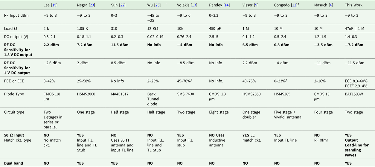
Adding more voltage-multiplying diode stages in PCB-based rectifiers or charge-pumps at low RF inputs offers some marginal increase in the DC output albeit at a big cost to efficiency due to more discrete diode losses. They are more common in WEHs where larger DC outputs are needed to be stored across an output energy-storing capacitor from low RF input power levels during charge cycles. The energy stored is for subsequent use to power heavier loads for limited duty cycles with the help of a parallel voltage supervisor or power management unit (PMU). These voltage supervisors and PMUs are typically voltage-controlled switches with a large off resistances between 10 kΩ and 10 MΩ (Rleak) during charge cycles to allow charge build-up across the energy storing capacitor. During subsequent active cycles, the PMU switch closes to allow the energy storage device to power a heavier load such as a fast microprocessor or sensor unit with regulation and on-off voltage hysteresis [10, 11]. In [Reference Congedo, Monti, Tarricone and Bella12, Reference Volakis, Olgun and Chen13], rectifying charge pumps with five and two stages are used to generate DC outputs of 1.8 V into output loads of 10 MΩ and 10 kΩ with RF inputs between −4 dBm (with antenna) and 0.8 dBm, respectively. By comparison, RF-DC charge pumps implemented using diode-FETS in CMOS have smaller sizes (<1 mm2) and losses, which allows for more stages and higher DC output voltages. In [Reference Masuch, Delgado-Restituto, Milosevic and Baltus6, Reference Pandey, Te Liao, Lingley, Mirjalili, Parviz and Otis14, Reference Li and Lee15], four–eight stage rectifiers generate DC outputs of 0.3–5 V in 2 kΩ–10 MΩ output loads with RF inputs between −9 and 3 dBm, and with RF-DC sensitivities of −3.5 to 2.2 dBm for 1.8 V DC output in the 2.4 GHz band.
RF-DC charge pumps with more stages are especially popular in 900 MHz radio frequency identification (RFID) integrated circuits (ICs) that use a large output energy storing capacitor in parallel with a large voltage-supervising resistive load (≥1 MΩ). These 900 MHz RFID ICs get DC outputs of 1 V or higher for RF inputs of less than −6 dBm, with which the RFID's logic controller and modulator can be powered for limited duty cycles without boost converters [Reference Hameed and Moez16]. Similarly, schemes at 2.4 GHz have been used in [Reference Visser, Pop, Vullers, Centre and Eindhoven5, Reference Congedo, Monti, Tarricone and Bella12, Reference Volakis, Olgun and Chen13] to increase DC output albeit at the cost of input match and efficiency at the higher frequency. Adding more diode-capacitor stages in RF-DC charge pumps tends to increase their input capacitance that makes matching to 50 Ω antennas challenging. The 900 MHz RFID ICs avoid this issue by requiring inductive antennas [Reference Hameed and Moez16]. However, in 2.4 GHz and higher bands, low-quality factors and high series resistance of inductors is a well-known issue, which results in lower efficiency and DC output.
B) Review of dual-band 2.4 and 5.8 GHz RF-DC rectifiers
In recent years, benefits of harvesting power from multi-band RF signals with a higher peak to average power ratios have been reported in getting higher DC outputs [Reference Valenta and Durgin2, Reference Boaventura and Carvalho17–Reference Collado and Georgiadis19]. A common challenge with multi-band wireless power harvesting tends to be matching inherently capacitive rectifiers with 50 Ω antennas in two or more bands. Solutions to this problem have been proposed above and in other works, which tend to be configured as shown in Figs 1(i) and 1(ii). A common method is using dual-band matching networks with a single half or 1-stage RF-DC rectifier that are terminated with optimal output loads of between 1 and 13 kΩ as shown in Fig. 1(i). Doing so has been found to improve return loss in dual frequency bands, and produce a PCE between 50 and 60% for input power of 0 dBm or higher [Reference Liu, Zhong and Guo20–Reference Suh and Chang22] (Table 1).
Dual-band RF-DC Rectifier Topologies. (i) Half-wave rectifier with dual-band matching network; (ii) single-band half-wave rectifiers or one-stage RF-DC voltage multiplier with matching networks in parallel; (iii) Proposed two-stage rectifier with no matching network.

Proposed rectifier's load-side transmission line dimensions on 0.02 inch FR4

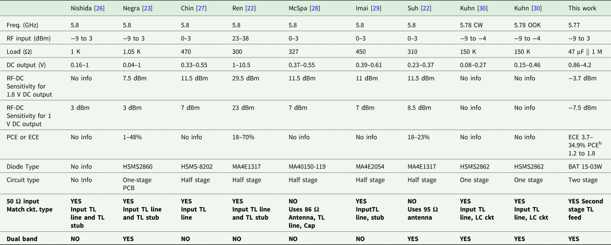
A second method is connecting two or more single-band matching networks with half or onestage charge-pumps tuned to different frequencies in parallel as shown in Fig. 1(ii) [Reference Hamano, Tanaka, Yoshida, Miyachi, Nishikawa and Kawasaki21–Reference Niotaki, Georgiadis, Collado and Vardakas24]. In [Reference Suh and Chang22], a topology like Fig. 1(ii) is used to get resonances at higher 2.4 and 5.8 GHz with peak PCE of 62% but at a higher 10 dBm of RF input into a 1 kΩ output load. The RF-DC sensitivities in these works are between 7.5 and 11.5 dBm at 5.8 GHz to generate a 1.8 V DC output with output loads between 470 Ω and 1.05 kΩ [Reference Suh and Chang22, Reference Wang and Negra23]. More detailed metrics on existing RF-DC rectifiers and charge-pumps in the 2.4 and 5.8 GHz bands can be found in Tables 2 and 3.
Performance comparison of 2.4 GHz RF-DC rectifiers

ECE, energy conversion efficiency for output energy storage loads; PCE, power conversion efficiency for output resistive loads.
a Includes antenna.
b PCE computed for load of 1 MΩ in parallel with 47 μF capacitor energy storage capacitor with insulation resistance of 50 Ω-F (1.06 MΩ).
Figures of Merit (FOM) in bold.
Performance comparison of 5.8 GHz RF-DC rectifiers

ECE, energy conversion efficiency for output energy storage loads; PCE, power conversion efficiency for output resistive loads.
aIncludes antenna.
b PCE computed for load of 1 MΩ in parallel with 50 Ω-F (1.06 MΩ) insulation resistance of 47 μF capacitor.
Figures of Merit (FOM) in bold.
C) Summary of proposed dual-band 2.4 and 5.8 GHz RF-DC rectifier design
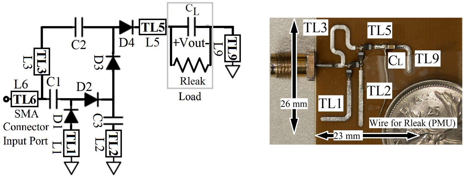
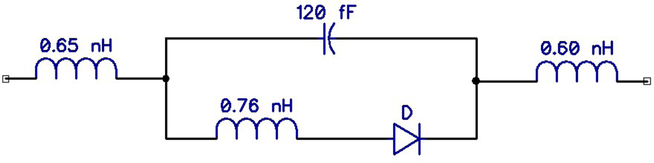
In this work, a novel, dual-band and two-stage RF-DC voltage-multiplying rectifier on PCB with higher RF-DC voltage conversion sensitivity, and with a 50 Ω input impedance without an external matching network in the 2.4 and 5.8 GHz bands is proposed as shown in Fig 1(iii), Fig. 2 and Table 1. There are two novelties in the proposed design. The first novelty is in the use of tuned transmission lines (TL 1, TL 2, TL 5 + TL 9) at the output of the rectifier's four half-stages to induce voltage standing wave peaks at the diode inputs (Fig. 2). Doing so increases the DC output of each half stage within the two-stage voltage multiplier topology, and across the output load capacitor while still giving the rectifier a near 50 Ω input impedance in the 2.4 GHz band. The second novelty is in the use of a tuned secondary feed (TL 3) to achieve dual-band return-loss resonance in the 5.8 GHz band without an external matching network. Simulations and measurements show this design needing lower RF input power of just −7.2 and −3.7 dBm at 2.4 and 5.8 GHz individually to generate 1.8 V across an output energy storage capacitor (C L) of 47 μF and a 1 MΩ voltage supervisor (PMU) load in parallel. The proposed design also generates a 3.5 V DC output with combined −3 dBm of RF input in both bands. The rectifier's higher DC output with a large output capacitor and PMU (R leak = 1 MΩ) allow heavy loads like a processor and sensor to run for limited duty cycles without an active DC–DC boost converter. Comparisons with other technologies in the table of comparison (Tables 2 and 3) show the proposed design having one of the highest RF-DC sensitivity at comparable input RF power levels and output loads in both the 2.4 and 5.8 GHz bands. Further test comparison of the proposed two-stage design with a conventional two-stage voltage multiplier with an external matching network and identical diode-capacitor components shows the proposed design generating consistently higher DC output voltage and having better immunity against changing output load resistance albeit at the cost of circuit size. Parasitics of the diode used in this work is shown in Fig. 3.
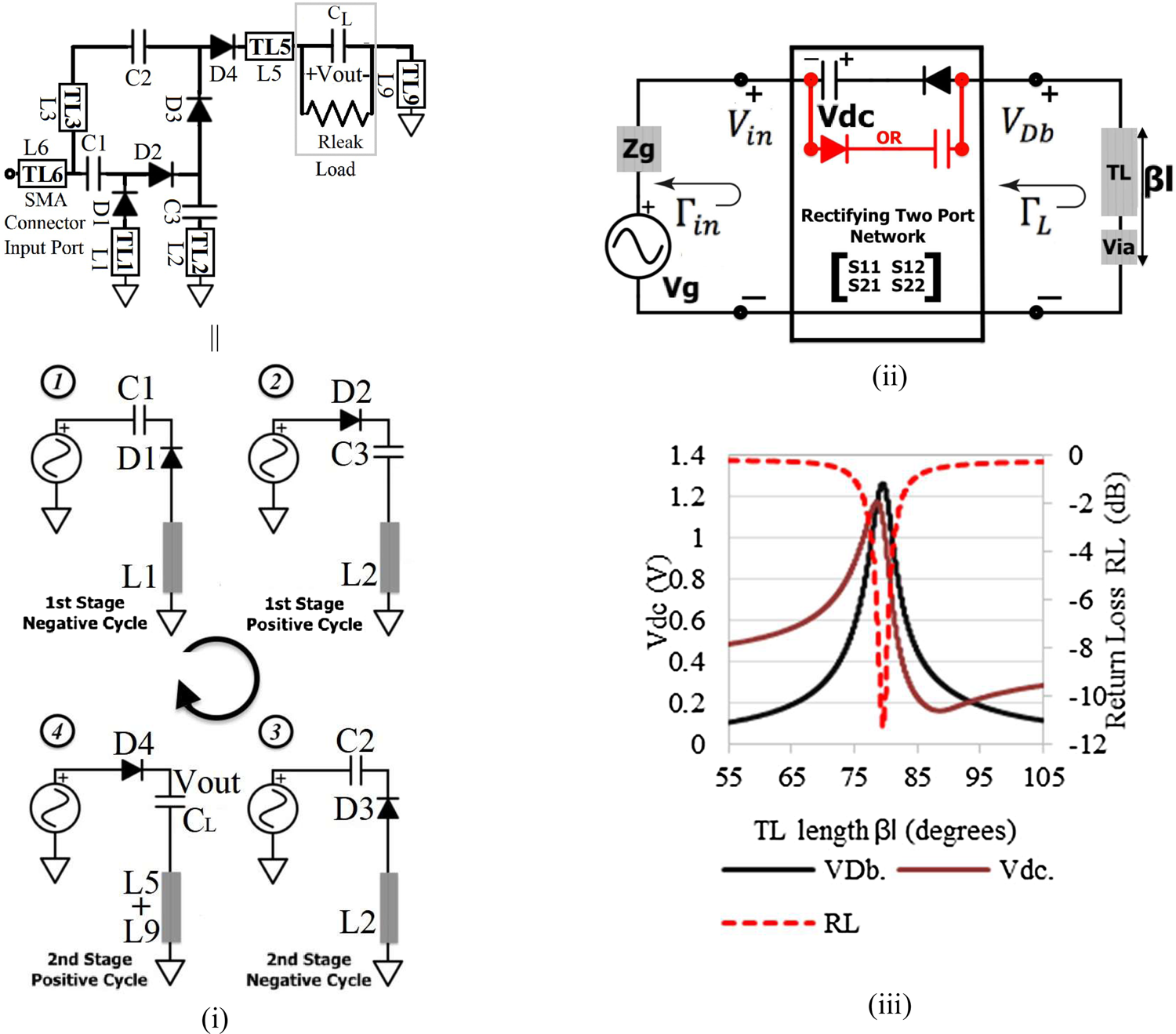
Proposed two-stage RF-DC voltage-multiplier circuit (rectifier) schematic & prototype designed on 0.02-inch FR-4. L 1–L 9 are optimized load-side TL sections in each rectifier stage. C 1–C 3 = 2 pF; C L = 47 μF; D 1–D 4:BAT1503W; Rleak = 1MΩ for Maxim 6461 Voltage supervisor (PMU) used.

BAT15-03W Diode RF Packaging equivalent circuit used in Agilent ADS simulations. Diode D Spice parameters IS = 74.0n N = 1.07 RS = 5.0 XTI = 1.5 EG = 0.59 + CJO = 138.5f M = 0.138 VJ = 0.224 FC = 0.5 TT = 3.0p BV = 4.2 IBV = 100.0u [31].

II. Theory and analysis
A) Theory of operation in 2.4 GHz band
1) Load-line optimization for DC output boost in rectifier stages
The two-stage rectifier's DC output voltage (V out) is the cumulative sum of the DC output of each of its four half-wave rectifiers i.e. DC voltages across C 1–C 3 and CP as shown in Fig. 4(i). To understand the effect of load lines in increasing the rectifier's DC output V out, consider the performance of each of its four half-stages, which can be modeled as a rectifying two-port network (RTPN) that is terminated with an optimally sized TL with electrical length β l as shown in Fig. 4(ii). The voltage output of the capacitor in the RTPN (V O) is the sum of its DC (V dc) and RF components (at frequencies ω c, 2ω c, 3ω c.) as in (1), where V dc depends on the voltage difference between output (V Db) and input (V in) of the RTPN as in (2). During each half cycle, maximizing V dc requires maximizing V Db, which depends on V in or the source voltage (V g), two port S-parameters (S 21 and S 22), output and input reflection coefficients (ΓL and Γin) of the RTPN as shown in (3)–(5)
 $$\eqalign{V_O & = V_{dc} + \displaystyle{{\vert {V_{Db}-V_{{\rm in}}} \vert } \over {K_1}}\sin (\omega _Ct) + \displaystyle{{\vert {V_{Db}-V_{{\rm in}}} \vert } \over {K_2}}\sin (2\omega _Ct) \cr & \quad + \ldots}$$
 $$V_{dc} = \displaystyle{1 \over {2\pi}} \mathop \int \limits_0^{\theta _{{\rm on}}} \! \vert {V_{Db}-V_{{\rm in}}} \vert \cdot \sin \lpar {\omega_Ct} \rpar d\lpar {\omega_Ct} \rpar $$
 $$V_{{\rm in}} = V_g/2\cdot \lpar {1 + \Gamma_{{\rm in}}} \rpar $$
 $$V_{Db} = \displaystyle{{V_g} \over 2}\cdot \displaystyle{{S_{21}\lpar {{\rm \Gamma}_L + 1} \rpar } \over {\lpar {1-{\rm S}_{22}{\rm \Gamma}_L} \rpar }}$$
 $${\rm \Gamma} _{{\rm in}} = S_{11} + \displaystyle{{S_{12}S_{21}{\rm \Gamma} _L} \over {1-S_{22}{\rm \Gamma} _L}}$$
 $$V_{dc-\max \;} \,{\rm and}\,V_{Db-\max} \,{\rm and}\,\Gamma _{{\rm in}-\min} \,{\rm for}\,\Gamma _L = \displaystyle{1 \over {S_{22}}}$$
(i) 4 Half-wave rectifying stages making up proposed 2-stage RF-DC rectifier. (ii) Each Half-wave rectifying stage modeled as a Rectifying 2-port network (RTPN). S 11 = S 22 = 0.94∠−19.63°; S 21 = S 12 = 0.34∠70.08° for BAT15-03W Diode and 2 pF Capacitor at 2.4 GHz. (iii) Simulated RTPN voltages at diode input (V Db) and Capacitor output (V dc); and input reflection co-efficient versus TL length (β l) at input frequency of 2.4 GHz.

For the rectifier's RTPNs, Infineon BAT15–03W RF diodes and 2 pF capacitor with a self-resonating frequency higher than 2.4 GHz were used. Using the diode manufacture's model and LSSP simulation tool in Agilent's ADS Software, S-parameters for the RTPN were determined for RF input power (P RF) of −6 dBm on a FR-4 substrate as shown in Fig. 4(ii). From (4), it is seen that the diode input (V Db) is maximum when ΓL = 1/S 22 = 0.94∠19.63° for a passive TL load. Having this complete impedance mismatch produces a maximum standing wave at RTPN's port 2, and a peak diode input (V Db) that is higher than the source voltage (V g). For a reasonably matched input, an RF input level of −6 dBm, and ΓL = 0.94∠19.63° yields a RTPN input (V in) of only 0.32 V but produces a diode input (V Db) of nearly 1.24 V using (5). Since the RTPN's capacitor nearly charges to V Db minus the diode's forward voltage, V dc is also maximized as a result as given by (2).
2) Load-line optimization for 50Ω input impedance in rectifier stages
To understand the effect of the load lines on the rectifier's input impedance, consider the working of its four RTPNs containing Diode-capacitor-TL pairs D 1-C1-L 1 (RTPN 1), D 2-C 3-L 2 (RTPN 2), D 3-C 2-L 2 (RTPN 3), and D 4-CL-L 5, L 9 (RTPN4) shown in Fig. 4(i) during each RF cycle. The input RF signal is rectified by RTPNs 1 and 3 only during negative RF cycles, and by RTPNs 2 and 4 only during positive RF cycles. It can also be seen from Fig. 4(i) that the total rectifier input impedance is the parallel combination of stage 1 (RTPNs 1 and 2) and stage 2 (RTPNs 3 and 4) through a common L 2 and C 3, which get used only during alternate half RF cycles. If the impedance of each of the RTPNs were near 50 Ω then RTPNs 1 and 2 in stage 1, and RTPNs 3 and 4 in stage 2 of the rectifier would yield close to a 25 Ω input impedance with little reactive part or a total return loss of 10 dB together during a full RF cycle.
To see if the impedance of each RTPN can be nudged to near 50 Ω by tuning its load-side TLs consider the RTPN as a two-port network as shown in Fig. 4(ii). With the diode capacitor pair's two-port gain given by S21 = S12 = 0.34∠70.08° at −6 dBm, the RTPN acts as a lossy two-port network with its input reflection coefficient given by (5). It can be seen from (5) that for ΓL = 1/S 22, the second term in (5) yields –S 11, thereby minimizing Γin and V in in (2) and (3). This is done by tuning the length of the via-shorted TL (∠ΓL and βl) such that ΓL = 1/S 22 = 0.94∠19.63°. Doing so also raises the RTPN's DC output (V dc) and overall rectifier's DC output voltage (V out) while minimizing the rectifier's input reflection coefficient.
The effect of the via-shorted TL length (βl) on the RTPN's Diode input V Db, DC output, V dc and input reflection co-efficient Γin on FR-4 (εr = 4.7) was studied using ADS's LSSP and Harmonic Balance tools as shown in Fig. 4(iii). Simulations show for an input voltage of 0.32 V (RF input power = −6 dBm), the RTPN gives a maximum output of V dc = 1.18 V (V Db = 1.23 V) with a minimum reflection coefficient of |Γin| = −11.52 dB (Γin = 0.1–j0.26) for an optimal TL reflection coefficient of ΓL = 0.97∠20.2° that is obtained for TL length of βl = of 80° at 2.4 GHz as shown in Fig. 4(iii). It should be pointed out that such an optimal TL load line works only with a WEH in which the input power is converted to energy in the output capacitor and loss through the diode and load-side TL. Doing so gives the RTPN and the proposed design a higher DC voltage and a 50 Ω impedance over time and in steady state.
3) Integration of rectifier half-stages into two-stage rectifier topology
The four RTPNs were combined into a single rectifier and optimized using ADS software with TL lines L 1, L 2, and L 5 + L 9 designed with a characteristic impedance of 50 Ω and an initial optimal length of 80° (14.7 mm) as per the RTPN analysis in Fig. 4(iii). To separate C L, L 5 and L 9 are set to 3.9 and 10.8 mm. The TL lengths were then iteratively tuned using ADS to adjust for parallel and series connections within the rectifier. The simulated effects of TL line lengths in the four RTPNs on the rectifier's overall DC output voltage (V out) is shown in Fig. 5, and shows a V out of 2.27 V for optimal lengths of L 1 = 78.8° (14.5 mm), L 2 = 71.7° (13.2 mm), and L 9 = 50.5° (9.3 mm). Optimal L 1 and L 2 lengths were observed to be a bit lower than a single RTPNs due to parallel connections within the rectifiers once the RTPNs are combined. The rectifier DC output V out was also observed to be more sensitive to L 1 and L 2 than L 5 + L 9 since harmonic balance simulation shows less RF component in the second stage of the rectifier. Due to the overall rectifier's and its RTPN's 50 Ω impedance, L 3 was also found to have less effect on V out in the 2.4 GHz band as shown in Fig. 5. However, tuning it appropriately was found to bestow dual-band characteristics to the charge-pump-based rectifier design as shown in the following section.
Simulated rectifier DC output (V out) versus TL line length (βl) at 2.4 GHz.

B) Operation in 5.8 GHz band
In this section, we show that dual band characteristics can be designed into the proposed 2-stage voltage-multiplier topology by tuning the secondary input feed L 3 that connects the charge-pump's input to its second stage as seen in Fig. 2. In the 2.4 GHz band (f 1), the two 50 Ω RTPNs in each of the rectifier's two stages conduct during each half of an RF cycle thereby giving each stage a 50 Ω impedance over a full cycle. With the two stages combined in parallel as shown in Fig. 6 and re-tuned to account for the parallel connection, the overall rectifier impedance is near 50 Ω as well (simulated reflection co-efficient = −9 dB). As a result L 3 has less of an effect on stage 2 and by it the rectifier's overall DC output (V out) in the 2.4 GHz band.
Total rectifier and its first and second stages acting in parallel at 5.8 GHz. Z t−f1: Total input impedance at 2.4 GHz; Z t−f2: Total input impedance at 5.8 GHz; Z 1−f1: Impedance of the first stage at 2.4 GHz; Z 1−f2: Impedance of the first stage at 5.8 GHz; Z 2−f1: Impedance of the second stage at 2.4 GHz; Z 2−f2: Impedance of the second stage at 5.8 GHz transformed by L 3; Z 2−f2−O: Impedance of the second stage with L3 = 0 mm.

However, in the 5.8 GHz band (f2), the rectifier's four RTPNs in the two stages shown in Figs 4(i) and 6 are expected to be non 50 Ω and of a capacitive nature. The total rectifier input impedance in the 5.8 GHz band (Z t–f2) is therefore approximately equal to the parallel combination of the impedance of its two-stages i.e. (Z 1−f2) and (Z 2−f2) through a common L 2 and C 3 that get used only during alternate half RF cycles as shown in Fig. 5 and determined using (6). L 1, L 2, L 5, and L 9 lengths were set to their optimum as shown in the previous section to maximize the rectifier's DC output, minimize input reflection co-efficient, and achieve a near 50 Ω input impedance in the 2.4 GHz band (Z t−f1). With these optimal line lengths connected to diodes D 1 and D 2 (Infineon BAT15-03W) and capacitors C 1 and C 3 (2pF each), the impedance of the rectifier's first stage was determined to be mostly capacitive as expected with Z 1−f2 = 1.3−j20.2 Ω at 5.8 GHz (f2).
 $$Z_{t-f2} = \displaystyle{{\lpar {Z_{1-f2}\cdot Z_{2-f2}} \rpar } \over {\lpar {Z_{1-f2} + \; Z_{2-f2}} \rpar }}$$
The rectifier's second stage is made up of capacitors C 2 (RF capacitor = 2 pF) and C p (larger energy storage capacitor = 47 μF) and diodes D 3 and D 4 (Infineon BAT15-03W) connected to TL L 5 + L 9, and a common L 2 also used by the first stage. A large PMU impedance (R leak) in the charge mode is also connected across C p. As a result, the impedance of the rectifier's second stage is also mostly reactive (Z 2−f2−O) as shown in Fig. 6(iii) and determined to be Z 2−f2−O = 1.2−j24.7 Ω using ADS. Next the length of L 3 (β lL3) was tuned to carry out an impedance transformation of the most reactive Z 2−f2−O such that the impedances of the first and second stage at 5.8 GHz i.e. Z 2−f2 and Z 1−f2 are conjugates of each other as shown in (7). Doing so cancels out the reactive component in the total rectifier impedance (Z t−f2) in the 5.8 GHz band as determined by (6).
 $$Z_{2-f2} = Z_{1-f2}^{^\ast} = Z_0\displaystyle{{Z_{2-f2-O}\; + \; j\cdot Z_0\cdot \tan \lpar {L_3} \rpar } \over {Z_0\; + \; j\cdot Z_{2-f2-O}\cdot \tan \lpar {L_3} \rpar }}$$
The effect of tuning L 3 on the impedances of the rectifier (Z t−f2) and its two stages (Z 1−f2 and Z 2−f2) in the 5.8 GHz band was simulated with the help of ADS software, which is shown in Fig. 7. The effect of varying L 3 between lengths of 0 (0°) and 20 mm (254°) on the rectifier's second stage impedance (Z 2−f2) is shown in Fig. 7, and shows it vary between a mostly reactive 1.2−j24.7 (Z 2−f2−O) and 10.7 + j81.6 Ω. The condition in (7) was met for L 3 = 3.6 and 17.2 mm, with the second stage having an impedance of 1.15 + j20 Ω and 3 + j20 Ω to the first stage impedance of 1.3–j20.2 Ω. At 5.8 GHz both Z 1−f2 and Z 2−f2 are mostly reactive and away from 50 Ω. However the parallel combination of Z 1−f2 and Z 2−f2 yields a mostly resistive Z t−f2 of 165.8 + j10 and 95−j4 Ω for L 3 = 3.6 and 17.2 mm, respectively, in the 5.8 GHz band as seen in Fig. 7. However, the shorter L 3 = 3.6 mm is too short to connect the rectifier's input port to C 2 in its second stage as seen in Fig. 2 hence L 3 = 17.2 mm was used. Starting with this initial length of L 3 = 17.2 mm in the overall rectifier design, L 3 was then re-tuned for maximizing the rectifier DC output V out.
Simulated and measured impedances of rectifier's first stage, second stage and overall input as a function of L 3 length. At 5.8 GHz: Z 1−f2 = 1.3−j20.2 Ω; Z 2−f2 = 3 + j20 Ω; Z t−f2 = Z 1−f2 || Z 2−f2 = 95−j4 Ω or Rectifier reflection co-efficient = −10.14 dB.

The simulated effect of L 3 on the rectifier's input reflection co-efficient and DC output (V out) is shown in Fig. 8(i), and shows a maximum V out of 1.11 V and return loss of −8 dB for an optimal L 3 = 17.8 mm with an RF input of −6 dBm. The effect of different L 3 line lengths on the rectifier's input return loss and V out as a function of frequency is also shown in Fig. 8(ii). It can be seen that increasing L 3 from its optimal length of L 3 = 17.8 mm has little effect on the return loss and DC output resonance in the 2.4 GHz band but produces a downward shift in resonance around the 5.8 GHz band justifying the dual band design principle of the proposed rectifier. The effect of varying L 3 on the rectifier's total input impedance, input reflection co-efficient and DC output voltage at 2.4 GHz (Z t–f1) is also shown in Figs 7 and 8(ii). They show the rectifier input impedance (Z t−f1) stay close to the 50 Ω region with very little change in the rectifier's return loss resonance and DC output voltage at 2.4 GHz. The measured total input impedance of the proposed rectifier in the 2.4 and 5.8 GHz bands for RF input power of −6 dBm have also been plotted in Fig. 7 for comparison.
(i) Simulated rectifier's input reflection co-efficient and DC output voltage (V out) versus L 3 line length at 5.8 GHz. (ii) Simulated rectifier's input reflection co-efficient and DC output voltage (V out) versus frequency.

The harmonic balance simulation of the rectifier's output showing the DC and RF components is shown in Fig. 9 below. The simulation show very little RF component present in both bands with most of the signal converted to DC at the rectifier's output. As a result, the rectifier's performance was found to be more sensitive to L 1, L 2, and L 3, and less sensitive to L 5 + L 9 and the output load. The increased sensitivity to L 1, L 2, and L 3 in the 2.4 and 5.8 GHz bands can also be seen in Figs 5 and 8(i).
Simulated DC and RF voltage components present at rectifier output with the following inputs. (i) 2.4 GHz source (ii) 5.8 GHz source.

III. Simulation and measurement results
A) Proposed rectifier performance versus frequency
The rectifier design was prototyped on 0.02-inch FR-4 due to its low cost and fast fabrication turn-around time as shown in Fig. 2. The rectifier's input reflection coefficient and DC output voltage were measured using a National Instruments PXI-E5632 VNA and Oscilloscope. A 1 MΩ output load (R leak) was connected across the output capacitor C L to emulate a PMU with 1 μA leakage current [10] and an initial RF input power of −6 dBm was supplied. Simulated and measured input reflection co-efficient and DC output of the rectifier are shown in Figs 10(i) and 10(ii), respectively. The dual band rectifier generates a DC output of 2.12 and 1.3 V, which agree well with the simulated values of 2.265 and 1.11 V in the 2.4 and 5.8 GHz bands, respectively. for input power of −6 dBm. Measured reflection co-efficient of less than−10 dB was also measured in both bands without the need for an external matching network. Simulations and measurements show good agreement in the 2.4 GHz band. The measured resonance of the rectifier was measured at a slightly lower 5.77 GHz compared to simulation, which can be attributed to the shift in FR-4's dielectric permittivity at higher RF frequencies. The proposed rectifier was prototyped on FR-4 using a very low-cost PCB process the dielectric constant of which can vary between 3.6 and 5.0 based on frequency and proportion of glass-resin epoxy content used in the FR-4 material [Reference Sarkar32, Reference Ritchey33]. The variation in the proposed rectifier's performance due to these different FR-4 dielectric constants have also been simulated and shown in Figs 10(i) and 10(ii). The shift in resonance in the 5.8 GHz band and the rectifier's overall performance can be improved by using a more stable and less lossy RF dielectric like Duroid.
(i) Rectifier's simulated and measured reflection coefficient versus frequency. (ii) Rectifier's simulated and measured DC output voltage versus frequency. RF input power = −6 dBm, PMU R leak = 1 MΩ. Eps represents the variation in FR-4's dielectric constant based on frequency and resin content reported in literature.

B) Measured verification of standing-wave in boosting rectifier DC output
In the proposed rectifier, load-side tuning of TLs L 1 and L 2 and to a lesser extent L 5 + L 9 boosts the voltage at the diode inputs (V Db) in each of its half wave rectifiers (RTPNs) by generating standing wave maxima at the diode inputs, which also increase the rectifier's DC output (V out). Tuning L 1 and L 2 also help achieve a reflection coefficient of −10 dB, which would also increase the rectifier's input power and consequently its DC output (V out). To verify the role of the standing wave in boosting V out, an Aaronia near-E-field probe and a Tektronics RSA 306B spectrum analyzer were used to measure the electric-field intensity that is proportional to the voltage along the length of lines L 1 and L 2 from the via ground right up until the input of diodes. With the contactless near-field probe and spectrum analyzer in peak hold, the electric field intensity proportional to the peak standing wave magnitude along the length of lines L 1 and L 2 can be gauged. These near-field measurements shown in Fig. 11 show the standing wave having minima near the via ground (electrical length = 0°) and close to maxima near electrical length of 78°–80° which is near the input of diodes D1 and D3. These maximas verify the role of the standing wave in boosting the rectifier output (V out).
Measured Electric field intensity versus electrical line lengths L 1 and L 2 of load-side TLs used in rectifier. The measured electric field intensity is proportional to the magnitude of voltage standing-wave at probe measurement points along lines L 1 and L 2. 0° is at via ground; 70°–80° is near D 1 and D 3 diode inputs for 2.4 GHz. The ripple in TL L 1 measurement is at its 90° bend shown in Fig. 2.

C) Proposed rectifier performance versus RF input power
The rectifier's DC output voltage and energy conversion efficiency (ECE) as a function of input RF power in the 2.4 and 5.8 GHz bands are plotted in Figs 12(i) and 12(ii), respectively. Since the bulk of the rectifier's RF input power is converted to energy stored across the output energy-storing capacitor CL as in a WEH, the rectifier's ECE was determined using (8). ECE is basically the power efficiency integrated over charge-up time (t) taken by the output energy storage capacitor (CL) to charge up to DC output voltage (V out). The rectifier's changing input impedance and reflection co-efficient over charge-up time (t) of the output energy storage capacitor (CL) is factored in the DC output voltage (V out) used to determine ECE. The DC output voltage across the capacitor reaches its maximum (V out) when the rectifier's total output current equals the current that leaks into the PMU's resistance (R leak) during charge modes as shown in other works [Reference Shigeta34, Reference Vyas, Cook, Kawahara and Tentzeris35]. As a result the effect of output PMU load R leak is also factored in the rectifier's DC output voltage V out. For the proposed rectifier the energy efficiency varied between 8.3 and 60% in the 2.4 GHz band, and between 3.7 and 34.9% in the 5.8 GHz band for RF input levels between −9 and 3 dBm. The DC output and efficiency in the 2.4 GHz band was higher than in the 5.8 GHz band due to a couple of reasons. Standing wave peaks along load lines (L 1, L 2, and L 5 + L 9) are designed to be induced at the diode inputs mainly in the 2.4 GHz band and not in the 5.8 GHz band. In addition, the diode reactances shown in Fig. 3 induce higher serial losses in the diode at the higher 5.8 GHz band. The dielectric losses on FR4 are also significantly higher at 5.8 GHz than at 2.4 GHz. As a result the RF-DC voltage conversion and efficiency in the 5.8 GHz band was lower than in the 2.4 GHz band. It should be pointed out that in both bands, addition of a second stage increases the DC output voltage obtained over time but lowers the ECE and PCE. This is due to addition of more series diode losses, which could be removed with the second stage albeit at the cost of RF-DC voltage conversion. The PCE of this circuit was also measured to be low since most of the output power goes into charging the output storage capacitor (C L) instead of being dissipated across the PMU leakage resistance (R leak).The peak ECE and PCE values are also shown in Tables 2 and 3.
 $${\rm ECE} = \displaystyle{{{\rm Energy\;} \,{\rm Stored}} \over {{\rm Input}\,{\rm Energy}}} = \; \displaystyle{{0.5 \times C_L \times V_{{\rm out}}^2} \over {P_{RF} \times t}}$$
(i) Simulated and Measured DC output voltage (V out) versus RF input power of proposed rectifier. (ii) Measured Energy efficiency (ECE) versus RF input power. C L = 47 μF, R Leak = 1 MΩ.

The novelty in the proposed work is in the use of load-side tuned TLs to induce standing wave peaks at the input of the diodes in a 2-stage voltage multiplying rectifier topology thereby boosting the rectifier's DC output voltage with a 2.4 GHz RF input. The measured effect of varying output load of a PMU (R leak) on the rectifier's DC output voltage and energy efficiency at different RF input power levels is shown in Fig. 13. The proposed rectifier's DC output voltage and energy efficiency holds up consistently for PMU load (R leak) of 90 KΩ and over where the PMU load is comparable to the energy storage capacitor's parasitic leakage resistance that typically is between 100 KΩ and 1 MΩ.
Simulated and Measured Rectifier DC output voltage (V out) and Energy Efficiency (ECE) for different rectifier output loads (PMU R leak).

Diode non-linearity is a known cause for impedance mismatches at low RF input levels. To study these effects with load-side TLs in the rectifier, its input reflection coefficient was measured for RF inputs of between −9 and 3 dBm as shown in Fig. 14. The rectifier shows a reflection coefficient of between −9 and −16 dB in the 2.4 GHz band and less than −10 dB in the 5.8 GHz bands for different RF input levels.
Measured input reflection coefficient versus frequency for different RF input power levels.

D) Comparison of proposed rectifier design using load-side lines with conventional two-stage voltage multipliers using matching networks
To further study the DC-output boosting advantages of using load-side tuned TLs in the proposed two-stage voltage-multiplying rectifier topology, a comparison was done with two conventional two-stage voltage-multiplying rectifiers without load-side lines. The designs were simulated using ADS. The two conventional rectifiers were designed without load lines but with optimal external matching networks and similar diode-capacitor pairs. The matching networks of the two conventional rectifiers were optimized for PMU loads (R leak) of 1 MΩ and 10 KΩ. Comparisons shown in Figs 15(ii) and 16(ii) show the proposed rectifier's input impedance much more immune to the effects of changing output PMU loads (R leak) and input power. This is due to the higher input voltage induced by the load sidelines at the diode inputs within the proposed rectifier topology mitigating diode non-linearity effects. As a result the proposed rectifier generated consistently higher DC output voltage compared to conventional two-stage rectifier for varying output PMU loads (Rleak) and RF input power shown in Figs 15(i) and 16(i), respectively. While the proposed rectifier was designed on PCB to demonstrate the benefits of load-side tuning in boosting the DC output in a two-stage voltage multiplier, this design technique can also be used in one-stage PCB-based or multi-stage CMOS-based voltage multipliers albeit at the cost of size of the TLs. Schematic used for the two-stage rectifier without load lines is shown in Fig. 17.
(i) Comparison of DC output voltages of proposed and conventional two-stage rectifiers for different output loads. (ii) Comparison of input impedance of proposed and conventional two-stage rectifiers for different output loads. Conventional rectifier input matching networks optimized for output loads of 10 KΩ and 1 MΩ. Proposed rectifier designed with load-side lines.

(i) Comparison of DC output voltages of proposed and conventional two-stage rectifiers for different output loads. (ii) Comparison of input impedance of proposed and conventional two-stage rectifiers for different output loads. Conventional rectifier input matching networks optimized for output loads of 10 KΩ and 1 MΩ. Proposed rectifier designed with load-side lines.

Simulated two-stage RF-DC voltage-multiplier circuit (rectifier) without load lines. L 1–L 9: Pads for SMT components. Matching circuit: C m = 1 pF, L m = 0.4 nH for R leak = 1 MΩ; C m = 1.22 pF, C m1 = 10.8 pF for R leak = 10 kΩ. C 1–C 3 = 2 pF; C L = 47 μF; D 1–D 4:BAT1503W.

e) Performance comparison of 2.4 and 5.8 GHz RF-DC rectifiers
Finally, a comparison of the proposed rectifier topology with other recent 2.4 and 5.8 GHz rectifiers capable of generating 1.8 V DC output is shown in Tables 2 and 3. Since RF-DC voltage conversion performance tends to be a function of input power, number of stages, input reflection co-efficient, output loads, we have included those metrics in the tables as well for a fair comparison. The comparison done so far shows that the use of a two-stage topology with the standing wave boost does improve the overall efficiency in league with other one-stage designs with a higher RF-DC sensitivity of −7.2 and −3.7 dBm for a 1.8 V DC output in the 2.4 and 5.8 GHz bands, respectively. Compared to other N-stage voltage multiplier topologies with identical output loads (100 KΩ or higher) in CMOS and PCB, the proposed design offers a higher DC output voltage and RF-DC sensitivity in both bands albeit at the cost of size due to the use of near quarter wavelength load-side TLs, and efficiency due to more series diode losses within rectifier's two-stage topology. It has been hard to do an apples to apple comparison since not many two or more stage rectifiers in these bands exist in the 2.4 and 5.8 GHz bands on PCB, and many works including the antenna gain in computing overall efficiency.
Conclusion
A novel, dual-band, two-stage RF-DC rectifier design with load-side tuned TLs in each of the rectifier stages to passively boost DC output and get reflection coefficient to under −10 dB without a matching network in the 2.4 band is presented. Additionally, by tuning the secondary feed in the proposed two-stage voltage multiplying rectifier topology, dual-band return loss resonance in the 5.8 GHz band is also achieved in addition to the 2.4 GHz band without an external matching network. A comparison of this design with other rectifiers shows the proposed design requiring a much lower RF input of −7.25 and −3.65 dBm to generate 1.8 V individually at 2.4 and 5.8 GHz while offering better immunity to changes in output load and input power levels compared to conventional rectifiers.
Financial support
This work was carried out at the University of Calgary with financial support from NSERC, Canada and equipment/tools support from CMC Microsystems, Canada.
Conflict of interest
None.
Ethical standards
No human and/or animal experimentation was involved in this work.
 Rushi Vyas received his B.Sc., M.Sc., and Ph.D. degrees in electrical and computer engineering from the Georgia Institute of Technology, Atlanta, GA, USA. He is currently an Assistant Professor in the Schulich School of Engineering, and a Researcher with the Pipeline Engineering Center (PEC), University of Calgary, Calgary, AB, Canada. His work has been covered in over 27 research publications in peer-reviewed journals and conference proceedings, and three book chapters covering topics in ambient RF -energy harvesting, inkjet-printed electronics, wireless gas and structural-health sensors, and real-time-localization systems (RTLS). Prior to joining academia, he worked on cellular radios at Apple Inc. and Blackberry. Prof. Vyas has received finalist and honorable-mention awards at the 2008 and 2012 IEEE International Microwave Symposia and the 2008 and 2009 IEEE Antennas and Propagation Society International Symposia (APS). His work on RF-energy harvesting and battery-less sensors has also been covered in media forums such as MSN News, Engadget, IEEE Institute, Energy Harvesting Journal, and New Energy and Fuel.
Sichong Li received his M.Sc. and B.Sc. in Eelectrical Eengineering from the University of Calgary and Beijing Institute of Technology, respectively. His research interests include antenna design and RF circuits.
 Fadhel Ghannouchi (S'84-M'88-SM'93-F'07) is currently a Professor, an Alberta Innovates/Canada Research Chair, and the Founding Director of the iRadio Laboratory, Department of Electrical and Computer Engineering, University of Calgary, Calgary, AB, Canada. He has held several invited positions with several academic and research institutions in Europe, North America, and Japan. He has provided consulting services to many microwave and wireless communication companies. He has authored or co-authored over 650 publications and holds 16 U.S. patents with four pending. His current research interests include microwave instrumentation and measurements, non-linear modeling of microwave devices and communications systems, design of power- and spectrum-efficient microwave amplification systems, and design of intelligent RF transceivers for wireless and satellite communications.