Introduction
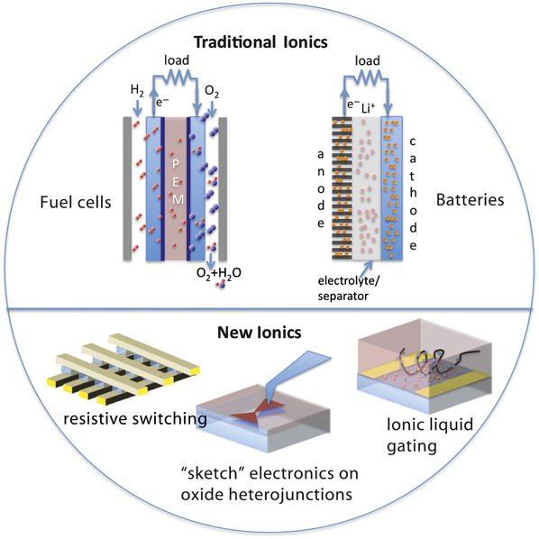
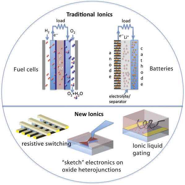
Ionic motion in bulk materials and at interfaces has played an enormous role in the development of many technologies.Reference Kim, Yamaguchi and Elliot1 The motion of ions in an electrolyte is essential for conventional batteries;Reference Huggins2 in solids, it is critical for the kinetics of lithiation and delithiation in modern lithium-ion batteriesReference Huggins2–Reference Goodenough and Kim5 (see schematic in Figure 1). Under discharge conditions, lithium ions diffuse through an electrolyte/separator from a Li-containing anode (shown schematically as Li-intercalated graphite). The electrolyte is pristine (in the case of solid electrolytes) or contains a macroscale ion-transporting separator that prevents direct electrical contact between anode and cathode. Lithium ions and electrons that have passed through the external load are reunited at the cathode, where lithium is intercalated into, or reacted with, the cathode material. In fuel cells, a solid material is often used as the electrolyte, acting as a transport medium for (negatively charged) oxygen anions or (positively charged) protons.Reference Minh6, Reference Steele and Heinzel7 As shown in Figure 1, molecular hydrogen is cracked catalytically at the anode, and protons diffuse through a macroscale proton exchange membrane (PEM) while electrons are transported through an external electrical load. The protons and electrons are united with oxygen species produced catalytically at the cathode to form water.
Top: Traditional ionics-based technologies. At left, a hydrogen fuel cell relies on ionic motion of protons through a proton exchange membrane (PEM). At right, a lithium-ion battery, which depends on ionic motion through the electrolyte and the separator. Bottom: New nano-based systems with behavior that is fundamentally ionic or electrochemical in nature. At left, resistive switching materials intended for use as non-volatile memories. At center, the creation of patterned electron gases at an oxide heterointerface due to local electrochemistry on the free oxide surface.Reference Cen, Thiel, Mannhart and Levy16 At right, the use of an ionic liquid to induce a very high density two-dimensional electron gas at an oxide surface (see Reference Reference Ueno, Nakamura, Shimotani, Ohtomo, Kimura, Nojima, Aoki, Iwasa and Kawasaki17).
In recent years, with our increasing ability to engineer materials at the nanometer scale, the motion of ions and the modification of surfaces via electrochemical reactions have become of increasing importance, even as their effects have sometimes been challenging to interpret. While these effects can complicate many situations, they also present new opportunities for materials engineering.Reference Maier8 Indeed, both ionic motion and electrochemical reactions have a greater impact at the nanoscale because of the same underlying physical reasons that have made nanoscale materials engineering so attractive: nanoscale materials generally have large surface-to-volume ratios. Chemical reactivity and defect motion at surfaces are both enhanced—or at least modified—from their bulk values. Changes in surface termination and charge can have profound effects on the electronic distribution in the comparatively small bulk, depending on electronic and dielectric screening. Modest voltages or differences in chemical potential across nanoscale distances can produce large electric fields and diffusive forces. In short, decreasing the characteristic scale of a system to the “nano” regime enhances ionic and electrochemical effects because driving gradients can readily become large, and the relevant length scale required for “interesting” ionic motion becomes small. Ions can move in response to these diffusive forces, and electrochemical reactions can become energetically favorable in the presence of altered ion concentrations and charge distributions.
Here we briefly review the present research status of several systems where ionic motion and electrochemical effects are particularly relevant (see Figure 1 for some representative examples of these systems). In particular, we discuss the physics and chemistry of resistive switching materials, the rapidly growing research in oxide heterostructures, the use of ionic liquids as tools to manipulate material properties, and ionic effects in ferroelectric materials. We will emphasize open questions regarding interpretation of experiments, which we believe need to be addressed to move the field forward. Finally, we will provide our outlook for future research directions.
Ionic conduction
Ionic motion is typically driven by an electrochemical potential difference, established through a concentration gradient and/or the application of an appropriate electrostatic potential difference (see Reference Reference Di Ventra9). The physical mechanism of ionic motion in a solid is often thermally activated hopping, with an activation energy determined by the detailed interaction of the ion with its surroundings.Reference Mehrer10 Typical point defects in crystalline solids involve such ionic motion; a Schottky defect is a vacancy in the lattice, while a Frenkel defect is a vacancy accompanied by an atom in an interstitial site. In typical Schottky or Frenkel defect motion, the activation energy can be on the order of a few electron volts.Reference Kittel11 In good ionic conductors, however, considerably lower activation energies are possible, particularly in systems with large amounts of open volume (e.g., glasses or glassy polymer networks).Reference Elliott12, Reference Armand, Bruce, Forsyth, Scrosati and Wieczorek13 Likewise, ionic transport may be favored by specific host crystal structures. For example, in rutile TiO2, the crystal structure has one-dimensional open channels extending along the c-axis.Reference Johnson, Paek and DeFord14, Reference Bates, Wang and Perkins15 This structure allows atomic hydrogen—protons, once the hydrogen’s electron is donated to the TiO2 conduction band—intercalated into those channels to diffuse rapidly along the channel direction. At the same time, the closeness of the Ti–O bonding network greatly restricts transverse diffusion of the protons. At room temperature, the anisotropy in diffusion constants exceeds 103 in this case.Reference Johnson, Paek and DeFord14 This particular example also highlights another subtlety peculiar to proton conductors. In the TiO2 case, the interactions between the proton and the host material are primarily hydrogen bonding with the oxygen atoms. This interaction is comparatively weak relative to a covalent bond and also does not strongly perturb the oxidation state of the host material.
Resistive switching: Ionic motion versus electrochemistry
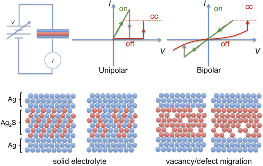
Resistive switching (RS) systems are outstanding examples of the occurrence of both ionic motion and electrochemistry at the nanoscale (e.g., see recent reviewsReference Waser and Aono18, Reference Pershin and Di Ventra19). A resistively switched material has electronic conduction characteristics that depend strongly on the past history of the voltage—or current—applied across the system. Typically a RS device, consisting of a source and drain electrode with intervening channel material, may be switched between two conducting states, “on”—relatively high conductance between the source and drain terminals—and “off”—relatively poor conductance—by the application of a suitable voltage ramp (see Figure 2). This change in conduction is nonvolatile, meaning that the RS device retains its state when the applied bias is reduced to zero. In a unipolar (bipolar) device, returning to the previous conductance state requires a voltage sweep of the same (opposite) polarity as the initial switching. The inherent hysteretic properties of RS systems have made them very attractive as a potential nonvolatile memory technology and for use in programmable logic arrays.Reference Strukov, Snider, Stewart and Williams20 In fact, these systems represent a particular case of a more general class of dynamical systems known as “memristors” (for memory resistors).Reference Pershin and Di Ventra19, Reference Chua and Kang21, Reference Di Ventra, Pershin and Chua22
Resistive switching. Top: Schematic of the essential two-terminal resistive switching device, consisting of source and drain electrodes sandwiching a resistive switching material. Two switching methodologies are paramount, unipolar switching (top center) and bipolar switching (top right). Bottom left: One type of unipolar switching is based on the switching material as a solid electrolyte, where local electrochemistry may convert metal ions into a conducting metal filament, as in Reference Reference Terabe, Hasegawa, Nakayama and Aono23. In that work, silver (blue circles) and sulfur (red circles) are the relevant materials, and the conducting filament forms by precipitation of Ag out of Ag2S. Bottom right: One proposed mechanism for some bipolar switching involves the bias-driven migration of oxygen vacancies to a particular electrode during the “set” process.

The idea that some materials can have resistive properties that depend on their electrical history is not a surprise to anyone who has ever seen the antistatic bags used to package electronic components. When the electric field across a dielectric material exceeds a critical “breakdown” threshold, the dielectric no longer acts as an insulator, and current may pass. Depending on the field, voltage, and current levels and the material itself, there can be a “hard” breakdown, resulting in a permanent, direct conducting path through the dielectrics, or “soft” breakdown, with defect-mediated conduction after bias-produced damage.Reference Alam, Weir, Bude, Silverman and Monroe61
The physical mechanisms behind the rich, varied RS phenomenology have been a challenge to sort out. It is clear from the nonvolatile nature of the switching that the root of RS lies in some chemical changes within the device; transient effects such as bias-driven injection of charge carriers to bring about an electronic transition would not result in state retention. Unipolar switching typically results from the formation of a conducting filament extending from one electrode to the other.Reference Waser and Aono18, Reference Sawa24 As bias voltage V is swept above a “set” threshold, the device makes a transition from a low conductance “off” state to an “on” state, where current is limited during formation by a current compliance. On a subsequent sweep to the same polarity, the conducting path is disrupted above a “reset” threshold (lower than the set voltage). The filament formation can be due to the migration of metal atoms—or ions—from the electrodes into the host material. Indeed, in nanoscale structures, extremely large electric fields at modest voltages are known to result in biased diffusion of mobile metal atoms.Reference Di Ventra9, Reference Korotkov, Bowman, McGuinness and Davidovic25
Alternately, conductive filaments may be formed by local redox chemistry—thermally and/or electrically assisted—at the electrode-channel or filament-channel interface. This is the physics and chemistry at work in the “soft” breakdown of dielectrics, for instance, and the embodiment that has received the most attention is TiOx-based memristors advanced by a group at Hewlett Packard.Reference Strukov, Snider, Stewart and Williams20 While this group has explained the switching mechanism of TiO2 based on oxygen vacancy motion, other mechanisms vie for contention. For example, other oxidation states of Ti are readily accessible, even though TiO2 is a comparatively stable, wide bandgap, high-κ dielectric. Once an electrochemical reduction (e.g., the local reduction of the TiIV oxide to the TiIII oxide) takes place at an electrode interface, the more reduced oxide is comparatively conducting and acts as a site of enhanced local electric field and potential where further chemistryReference Wu and McCreery26 may occur.
When a charge carrier must move from a metal into a semiconductor or other dielectric, there is often an energetic mismatch between the highest occupied electronic level in the metal and the energy of the lowest unoccupied state in the other material at the interface. Then, this mismatch of energies across the interface is an effective barrier to transport of charge, called a Schottky barrier. Another possible mechanism in resistive switching is for local electrochemistry at the interface to modify the energetic alignment, modulating the Schottky barrier height at the interface.Reference Jeong, Schroeder and Waser27
A switching mechanism similar to the TiO2 case takes place in the Ag2S/Ag system, another candidate resistive switch proposed for nonvolatile memory and logic applications.Reference Terabe, Hasegawa, Nakayama and Aono23 Here, the sulfide acts as a solid electrolyte, allowing the diffusion of Ag+ ions, with their subsequent reduction under bias leading to the formation of a silver nanowire. In these unipolar devices, switching into the “off” state requires thermal disruption of the conducting path, through local Joule heating under bias.
It is worth noting that qualitatively and quantitatively similar resistive switching phenomena have been observed in many nanoscale devices,Reference Yao, Zhong, Zhang, He, Jin, Wheeler, Natelson and Tour28 including those containing molecules or molecular layers as the intended active region.Reference Tour, Cheng, Nackashi, Yao, Flatt, St. Angelo, Mallouk and Franzon29 This again reinforces the notion that biases of a few volts applied over distances in the few nanometers regime can be sufficient to induce resistive switching processes in substrate oxides that may otherwise be intended to function as inert bystanders. This is so even in very stable oxides such as SiO2.Reference Yao, Sun, Zhong, Natelson and Tour30, Reference Yao, Zhong, Natelson and Tour31 High electric fields exceeding macroscopic breakdown thresholds alone are not sufficient to lead to these effects: carriers still require sufficient energy at their disposal to alter chemical bonds.
In bipolar resistive switching, resetting from the “on” to “off” states requires sweeping the bias to the opposite polarity, indicating an inherent asymmetry in the nature of the switching material in the “on” state. Many bipolar RS devices, particularly those based on complex oxides such as perovskites, appear to rely directly on the electric field- and bias-driven diffusion of oxygen vacancies or ions within the oxide matrix for their operation.Reference Waser and Aono18, Reference Sawa24 In these systems, the dominant contribution to the total device resistance is the Schottky barrier at the interface between the electron-injecting source and the oxide channel. The interplay between these vacancies and the conduction properties depends strongly on the nature of the oxide. One particular example is the case of Pr0.7Ca0.3MnO3, a p-type oxide (see Reference Reference Sawa24 and references therein). Applying a bias of one polarity drives vacancy migration away from the interface, lowering the local Schottky barrier and decreasing the width of the depletion region, thus enhancing conduction. Conversely, a bias of the opposite polarity accumulates vacancies at the electrode-oxide interface. Once there, these vacancies increase the local Schottky barrier as well as the width of the depletion region within the channel material.
Oxide heterostructures and superconductivity
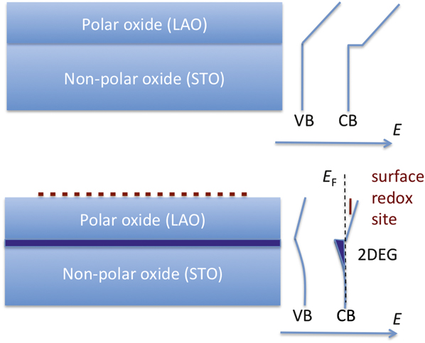
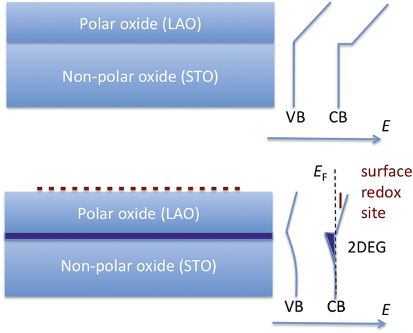
Oxygen defects have also proven to be of great importance in oxide heterostructures. In cuprate-based high-temperature superconductors, deviations in oxygen stoichiometry from that of the parent cuprate perovskites have been used as a doping technique to tune carrier concentration and hence superconductivity.Reference Cava, Batlogg, Chen, Rietman, Zahurak and Werder32 In oxide heterostructures, techniques such as pulsed laser deposition and molecular beam epitaxy have been used to grow planar heterojunction interfaces between different oxides. At these interfaces, layers of electrons (“two-dimensional electron gases”) accumulate, mobile in the plane of the interface, but trapped in the third dimension by the internal electric fields within the oxides (see schematic band structure in Figure 3). It should be no surprise that recent experiments in the growth of such oxide heterostructures have revealed that oxygen vacancies and excess oxygen at the heterointerfaces can contribute significantly to the density and properties of these two-dimensional electron gasesReference Schneider, Esposito, Marozau, Conder, Doebeli, Hu, Mallepell, Wokaun and Lippert33 (see schematic in Figure 3). Depending on the type of substrate, the temperature dependence of the sheet resistance of a SrTiO3 film grown by pulsed laser deposition can range from metallic to insulating.Reference Schneider, Esposito, Marozau, Conder, Doebeli, Hu, Mallepell, Wokaun and Lippert33 Mass spectrometry reveals interdiffusion of oxygen at the growth interface between the substrate and the growth layer, demonstrating the importance of oxygen and oxygen vacancy motion in these materials. Studies of superconductivity in these structures show that these oxygen defects are not solely responsible for conduction,Reference Reyren, Thiel, Caviglia, Kourkoutis, Hammerl, Richter, Schneider, Kopp, Ruetschi, Jaccard, Gabay, Muller, Triscone and Mannhart34 but neither can they be neglected.
The importance of surface electrochemistry in oxide heterostructures. As discussed in Reference Reference Bristowe, Littlewood and Artacho35, the upper oxide in the much studied SrTiO3/LaAlO3 (STO/LAO) heterojunction system is polar. With no compensation, the electrostatic potential of the free oxide surface would climb as the LAO thickness is increased, reaching electrochemically significant levels after only a few unit cells. Surface redox chemistry alters the band energetics, partially compensating this potential, leading to the formation of a two-dimensional electron gas confined at the STO/LAO interface, represented by the dark blue layer. This is suggested as the basis of the ability to modify the electron gas on demand via surface electrochemistry.Reference Cen, Thiel, Mannhart and Levy16, Reference Xie, Bell, Yajima, Hikita and Hwang36, Reference Bi, Bogorin, Cen, Bark, Park, Eom and Levy37 VB, valence band; CB, conduction band; E, energy; E f, Fermi energy level; 2DEG, two-dimensional electron gas.
Oxide heterostructures are also an excellent example of the importance of interfacial electrochemistry. In conventional semiconductor heterointerfaces, such as those based on modulation-doped AlGaAs/GaAs, a two-dimensional electron gas may also be formed, with electrons confined to the interface.Reference Weisbuch and Vinter38 Through the use of metal gates or surface etching on the exposed top surface of the material, it is possible to deplete this electron gas via electrostatic interactions. This technique is at the heart of modern experiments on gate-defined quantum dots.
In SrTiO3/LaAlO3 (STO/LAO) heterojunctions (as in Figure 3), similar effects have been observed when a conducting tip is used to “poll” the exposed oxide surface.Reference Cen, Thiel, Mannhart and Levy16 Applying this potential leads to the nonvolatile accumulation of conducting electron gas at the interface below the tip. Much attention has been paid to the idea of “Etch-a-Sketch” oxide electronics, nicknamed after a popular toy in which a child can draw, erase, and redraw pictures, with the possibility of fabricating reconfigurable electronic devices via “drawing” with a conducting tip. At the root of this writing phenomenon is the electrochemical alteration of the surface of the oxide.Reference Xie, Bell, Yajima, Hikita and Hwang36, Reference Bi, Bogorin, Cen, Bark, Park, Eom and Levy37 Local redox chemistry performed by the tip on the exposed oxide surface can act as an effective gate on the underlying oxide interface, tuning the local charge density by as much as ∼1013 carriers per cm2.
In this case, it is thoughtReference Bristowe, Littlewood and Artacho35 that the sensitivity to the surface charge results from the polar nature of LAO, starting from the nonpolar STO layer. In the absence of other effects, growing successive unit cells of LAO would lead to a steadily increasing electrostatic potential across the LAO. After a few unit cells, it becomes energetically favorable to compensate this potential somehow, such as through oxygen defects or chemical modification of the free LAO surface. Because of this physics, the surface charge of the free LAO interface has a direct impact on the energetics of the buried LAO/STO interface.
Ionic liquids
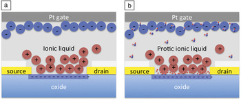
The type of interfacial chemistry described in the preceding section is not limited to oxide heterostructures. Recent workReference Yuan, Shimotani, Tsukazaki, Ohtomo, Kawasaki and Iwasa39 by Yuan et al. explored “protic ionic liquids,” ionic liquids that contain dissolved, dissociated water, as a means of gating the charge density in field-effect-style devices (Figure 4). Rather than working with a conventional gate dielectric, the researchers employed an ionic liquid, essentially a liquid organic salt, as a gate medium. By applying a voltage—relative to the source and drain electrodes—to an immersed platinum coil as a counter-electrode, constituent ions in the ionic liquid are driven to the channel material interface. To compensate for this ionic surface charge, mobile carriers in the channel material need to accumulate to densities that may exceed 1014 cm−2. In the protic ionic liquid case, water dissolved in the ionic liquid was dissociated electrochemically into H+ and OH− ions.
Ionic liquids for field-effect devices. (a) An ionic liquid is used as an electrolytic gate. A bias applied to the counterelectrode produces an accumulation of ions right at the channel/liquid interface. In the absence of large surface state effects, the resulting enormous interfacial electric field is compensated by the accumulation of an extremely large surface charge density in the channel, approaching or even exceeding one charge carrier per unit cell. (b) The situation in a protic ionic liquid. As shown, hydronium ions dissolved in the ionic liquid are forced to the channel/liquid interface; under appropriate surface chemistry conditions, the protons may bind to the channel surface, supplementing the ionic liquid’s charge accumulation effects with those associated with the proton attachment.
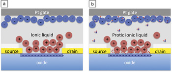
With a positive bias applied to the Pt, the H+ ions were pushed to the channel material interface and adsorbed, protonating the surface. With ZnO as the channel, the authors observed enormous gated charge densities for the oxygen-terminated ZnO surface, ascribed to the chemical bonding of the protons to the terminating oxygens.Reference Yuan, Shimotani, Tsukazaki, Ohtomo, Kawasaki and Iwasa39 Because of the strength of this interaction, the protonation was found to be hysteretic under sweeping of the gate potential, nonvolatile in a similar fashion as in the LAO/STO system. Conversely, for the Zn-terminated surface, large charge densities of the opposite sign were possible with surface accumulation of OH− ions, though hysteresis was much less pronounced, as these ions were apparently physisorbed via weaker interactions.
Closely related to this work, Ohta et al. have recently demonstratedReference Ohta, Sato, Kato, Kim, Nomura, Ikuhara and Hosono40 the deliberate use of water (rather, the H+ and OH− ions produced by its electrolysis) as a means of gating the STO surface into metallicity. By using a water-infiltrated, nanoporous glass as a gate dielectric, they used the gate bias associated with the field effect to split the water right at the dielectric/STO interface, leading to the accumulation of extremely large surface charge densities exceeding 1015 cm–2. While packaging may be a serious issue standing in the way of the application of this approach, this is a remarkable example of deliberate nanoscale control over electrochemistry, for the purpose of employing the ions thus produced to modify an electronic material.
Ionic liquids themselves provide a means of achieving tunable, large accumulated carrier densities in transistor-like structures. Thanks to the broad window of electrochemical stability for these liquid salts, surface carrier densities approaching or exceeding one charge per surface unit cell are possible. This has led to a dramatic flurry of experiments, including the gating of strontium titanateReference Ueno, Nakamura, Shimotani, Ohtomo, Kimura, Nojima, Aoki, Iwasa and Kawasaki17 and other layered compoundsReference Ye, Inoue, Kobayashi, Kasahara, Yuan, Shimotani and Iwasa41 from insulating to metallic to superconducting states, and the “turning-on” of high-temperature superconductivity via electrostatic doping of ultrathin cuprate layers.Reference Bollinger, Dubuis, Yoon, Pavuna, Misewich and Bozovic42, Reference Leng, Garcia-Barriocanal, Bose, Lee and Goldman43 These works hold out the prospect of controlled migration of ions as a new tool in the exploration of fundamental materials physics.
Ferroelectrics
Ferroelectrics are yet another type of material where ion dynamics play a crucial role. In these materials, the ferroelectric polarization originates through displacement of ions within the unit cell, and the stable polarization states reflect the presence of a double-walled potential for those ions within the unit cell. (This is in contrast to the ionic systems in previous sections, where inter-unit cell or long distance motion of ions is central to the phenomena described.) Polling the ferroelectric material via an externally applied electric field causes motion of the ions from one local potential minimum to the other within the unit cell. The stability of the ferroelectric polarization state following the material’s exposure to externally applied electric fields makes these materials good candidates for possible use in memories. For instance, the ability to tune the average electric polarization of a ferroelectric material by an electric field is now used in ferroelectric random-access memories (FeRAMs) with functionalities similar to flash memories.Reference Scott and Paz de Araujo44
Of particular interest is the proposal of exploiting tunneling across an ultra-thin ferroelectric layer sandwiched between two metallic leads to obtain variable resistance that is also reversible.Reference Tsymbal and Kohlstedt45 In this case, when the electric field applied to the film exceeds the coercive field of the ferroelectric, collective ionic displacement can take place which, in turn, changes the energetic barrier for electron tunneling, thus varying the resistance of the junction. Precisely because ferroelectricity is a collective phenomenon, it should break down at some critical thickness. The remarkable finding is that the thickness of the ferroelectric layer can be made as small as a nanometer (e.g., by employing highly strained films of BaTiO3), still allowing non-destructive resistive readout.Reference Garcia, Fusil, Bouzehouane, Enouz-Vedrenne, Mathur, Barthelemy and Bibes46 This is a major finding that could lead to FeRAMs with higher densities and faster operation than flash memories.Reference Garcia, Fusil, Bouzehouane, Enouz-Vedrenne, Mathur, Barthelemy and Bibes46 A better understanding of how the interplay between tunneling, strain, and electron-ion scattering induces ionic collective displacement at the nanoscale would be desirable.
However, as in the oxide heterostructure systems discussed previously, the presence of large electrostatic energy scales at surfaces and interfaces due to polarization can lead to further complications due to redox chemistry at surfaces. This has been explored in some detail recently by a group from Oak Ridge National LaboratoryReference Kalinin, Jesse, Tselev, Baddorf and Balke47 in the context of scanning probe microscopy of ferroelectric surfaces. That work shows how the combination of bias application and force detection under various environmental conditions (humidity, bias rates) can allow the delineation of the different polarization, ion motion, and electrochemical processes at work at oxide interfaces. Recent theoretical workReference Bristowe, Stengel, Littlewood, Pruneda and Artacho48 establishes that redox processes at the surfaces of ferroelectric layers as thin as 1 nm can stabilize polarization states that would otherwise not remain fixed in the absence of the chemically modified surface charge. In general, the electrochemical environment can alter the balance between competing polarization states and unpolarized phases.Reference Stephenson and Highland49
Previous hints of such interfacial chemistry have been observed in apparent ferroelectric switching of the conductance in perovskite nanotubes,Reference Nonnenmann, Gallo and Spanier50 where oxygen vacancy migration driven by such electrostatics is thought to be relevant. A careful series of measurements involving annealing in various oxygen environments clearly shows the critical role of oxygen in the observed electroresistive effects.
Similarly, it has been known for some timeReference Wehling, Novoselov, Morozov, Vdovin, Katsnelson, Geim and Lichtenstein51 that charged and polar adsorbates can act to shift the electrochemical potential in graphene layers, altering the threshold voltage as an effective gate. Recently, investigatorsReference Hong, Hoffman, Posadas, Zou, Ahn and Zhu52 have found that water dissociation driven by the energetics of ferroelectric gate interfaces can be employed to engineer these threshold effects deliberately, possibly forming the basis of nonvolatile memories based on this effect.
Conclusions and outlook
Through the examples discussed here, it should be clear that ionic motion and electrochemistry can play essential roles in nanoscale devices, whether or not such processes were originally intended to be part of the device functionality. In hindsight, this should not come as a surprise: Nanoscale structures have enhanced surface effects and susceptibility to defect or impurity motion on surface/volume grounds alone. With inherently small length scales, modest concentration or potential differences result in large chemical potential gradients to support diffusive and chemical processes. In polar and ferroelectric materials, uncompensated polarization can favor interfacial electrochemistry to compensate what would otherwise be locally large unscreened electric fields, with results that can be dramatic.
Nevertheless, it is important to stress that the widespread occurrence of ionic and electrochemical phenomena in nanostructures is sure to be leveraged in novel applications. The tuning of electron gases at oxide heterojunctions has already been proposed for device engineering;Reference Cen, Thiel, Mannhart and Levy16 now that the surface electrochemical nature of the mechanism is becoming better understood, such structures have been suggested as sensors.Reference Xie, Hikita, Bell and Hwang53 Similarly, the surface modification of oxides via protonation, achieved electrochemically using “protic” ionic liquids,Reference Yuan, Shimotani, Tsukazaki, Ohtomo, Kawasaki and Iwasa39 is a novel approach for the alteration of electronic properties of oxides, falling in between field effect and chemical doping. The related use of hydrogen as a dopant in nanomaterials has recently been put forward as a means of modifying the electronic and optical properties of TiO2 to tune its use as a photocatalyst into the visible part of the spectrum.Reference Chen, Liu, Yu and Mao54, Reference Wang, Wang, Ling, Tang, Yang, Fitzmorris, Wang, Zhang and Li55
Finally, nanoscale ionic motion and electrochemistry are receiving the most attention in the quest for novel battery materials.Reference Bruce, Scrosati and Tarascon56, Reference Armand and Tarascon57 Lessons are being learned in the studies of such systems, including microscopic changes in the morphology of nanomaterials upon ionic intercalation,Reference Liu, Zhang, Zhong, Liu, Zheng, Wang, Cho, Dayeh, Picraux, Sullivan, Mao, Ye and Huang58, Reference Liu, Zheng, Zhong, Huang, Karki, Zhang, Liu, Kushima, Liang, Wang, Cho, Epstein, Dayeh, Picraux, Zhu, Li, Sullivan, Cumings, Wang, Mao, Ye, Zhang and Huang59 and the development of in situ observational methods to examine nanomaterial/electrolyte interfaces. While the motivations for battery research are obvious, techniques developed in this area may prove very useful as more general attempts are made to understand and take advantage of the unique opportunities presented by ionic and electrochemical effects in electronically active nanostructures. As an example, we mention a fertile and important area of research that is gaining considerable attention: DNA sequencing and detection.Reference Zwolak and Di Ventra60 Here, the interplay between ionic motion and electrochemistry at the interface between water and metal probe surfaces is still not fully understood. Efforts in this direction will definitely contribute to the realization of fast and low-cost sequencing devices.
Acknowledgments
D.N. acknowledges partial support from the Department of Energy Basic Energy Sciences grant DE-FG02–06ER46337. M.D. acknowledges partial support from the NSF grant No. DMR-0802830 and UC-Labs.
Douglas Natelson Department of Physics and Astronomy, MS 61, Rice University, 6100 Main St., Houston, TX 77005, USA; and email natelson@rice.edu.
Natelson is a professor of physics and astronomy and in electrical and computer engineering at Rice University. He arrived at Rice after a postdoctoral stint at Bell Labs, after earning his PhD degree from Stanford University in 1998. His research group focuses on experimental condensed matter physics at the nanoscale, including electronic and optical properties of atomic- and molecular junctions, nanostructures made from strongly correlated materials, and organic semiconductors. Natelson has published more than 70 reviewed papers and blogs about nanoscale science at nanoscale.blogspot.com.

Massimiliano Di Ventra Department of Physics, University of California San Diego, La Jolla, CA 92093–0319, USA; tel. 858–822–6447; and email diventra@physics.ucsd.edu.
Di Ventra has been a professor of physics at the University of California, San Diego, since 2006. He graduated from the Ecole Polytechnique Federale de Lausanne (CH) in 1997. His main research interest is in the theory of electronic and transport properties of nanoscale systems. Di Ventra has published more than 140 refereed papers and has delivered more than 140 invited talks worldwide on these topics. He has co-edited the textbook Introduction to Nanoscale Science and Technology (Springer, 2004) for undergraduate students, and he is the author of the graduate-level textbook Electrical Transport in Nanoscale Systems (Cambridge University Press, 2008).