I. INTRODUCTION
The power amplifier (PA) is one of the most critical blocks of any wireless transmitter chain. The PA is responsible for boosting the delivered output power while operating with high-power efficiency and preserving the signals' integrity. With the evolution of wireless systems during the last decades, the requirements in terms of output power and efficiency have become stricter. This has forced the investigation of new semiconductor technologies in the microwave context. Particularly, since gallium arsenide (GaAs)-based transistors have reached their limits, the attention has been focused on gallium nitride (GaN)-based microwave active devices [Reference Zolper1, Reference Trew2]. Owing to the wide band gap, GaN provides excellent features for high-power applications in the microwave field and has been recognized as the most promising candidate to reach the output power requirements. However, not being a mature technology, a lot of effort has been put to characterize the behavior of GaN-based devices due to the presence of defects in the materials which strongly influence the performance, like for instance the maximum achievable output power [Reference Binari, Klein and Kazior3, Reference Ventury, Zhang, Keller and Mishra4]. Moreover, due to reliability issues, it is important to monitor the evolution of the signals exciting the active device. As a consequence, the characterization of the behavior of GaN transistors, as possibly close to realistic operating condition, is a fundamental step. Among the different characterization techniques employed, the one based on high-frequency (HF) nonlinear measurements has attracted the interest of researchers in the last decades. Although it relies on expensive equipment, like the large-signal network analyzer (LSNA) [Reference Verspecht5], it allows the characterization of any active device under realistic conditions, in the microwave frequency range and under high-power excitations. Load-pull (LP) measurements, or more generally waveform engineering [Reference Tasker6] techniques, are widely exploited to synthesize realistic source and load terminations to achieve the operating condition that maximizes the output power and the efficiency. As such, the LP technique constitutes a powerful tool not only for the design of PA but also for the dynamic characterization of active devices. However, due to the HF operation, the parasitic network and the reactive nonlinearities shape the load line at the device measurement planes thus hiding the load line at the intrinsic current generator plane. Such information is of great interest in PA design, since all design techniques, from class-A to high-efficiency classes [Reference Cripps7], are based on the correct definition of the optimum impedances at the device's intrinsic current source (i.e. the device resistive core [Reference Raffo, Scappaviva and Vannini8, Reference Raffo, Vadalà, Di Falco, Scappaviva and Vannini9]). In addition, loading conditions providing similar microwave performance may correspond to load lines, at the intrinsic resistive core, with different shapes, which can show very different robustness in terms of reliability constraints (e.g. breakdown). Consequently, in order to accurately define the optimum condition for device operation, the load lines measured at the accessible terminals have to be shifted back to the resistive-core planes.
The method presented in [Reference Raffo, Scappaviva and Vannini8, Reference Raffo, Vadalà, Di Falco, Scappaviva and Vannini9] relies on a low-frequency time-domain LP system which directly provides the load line at the intrinsic resistive core and combines it with a model-based description of parasitic network and strictly dynamic nonlinearities. In this way, the information at the intrinsic device plane is moved toward the extrinsic one. In this work a de-embedding technique starting from vector HF measurements is proposed. This technique, combined with an accurate description of the parasitic network and the reactive nonlinearities, allows one to obtain the information about the load line at the intrinsic resistive core directly from large signal measurements performed in the microwave range. The work is outlined as follows: in Section II the proposed technique is described, Section III is devoted to the obtained experimental results and the discussion. Finally conclusions are drawn.
II. THE PROPOSED DE-EMBEDDING PROCEDURE
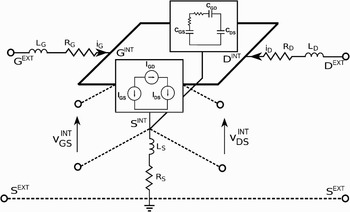
The approach proposed in this work relies on the model topology reported in Fig. 1. With no loss of generality a common source configuration is considered. The model in Fig. 1 can be divided into two sections: an extrinsic one which accounts for the parasitic network and the intrinsic one which models the active area of the semiconductor device. The latter can be further split into a resistive core that includes the current generators and describes the static and low-frequency I/V characteristics, and a capacitive core that accounts for the purely dynamic contribution to the device current due to reactive effects in the presence of very fast-varying signals. It is worth noticing that, in order to guarantee accurate prediction capability, the capacitive core description should properly account for non-quasi-static effects.
Equivalent circuit topology as considered in this work.

This separation into a resistive and a capacitive core is common in the semiconductor area and is the mostly employed in literature [Reference Filicori, Santarelli, Traverso, Raffo, Vannini and Pagani10–Reference Curras-Francos, Tasker, Fernandez-Barciela, Campos-Roca and Sanchez12]. Moreover, two different reference planes are defined within the schematic of Fig. 1. The extrinsic plane defines the measurement plane where the probe tips are physically placed. At this plane, the measured phasors of the voltages and currents include the mixed influence of the active core and the parasitic network. On the other hand, the intrinsic plane delimits the device active area where the performance achievable by a selected technology is defined.
The first step of the proposed procedure consists of shifting the measured spectra up to the intrinsic planes. This step [Reference Tasker6, Reference Raffo, Scappaviva and Vannini8, Reference Wright, Sheikh, Roff, Tasker and Benedikt13] requires an accurate description of the parasitic networks (including the device package) which is obtained through S-parameter measurements by exploiting widely known techniques based on lumped elements approximation (e.g. [Reference Dambrine, Cappy, Heliodore and Playez14]), or, alternatively, by adopting electro-magnetic simulations of the device layout (e.g. [Reference Resca, Raffo, Santarelli, Vannini and Filicori15]). This step can be accomplished straightforwardly by applying a linear transformation in frequency domain, as expressed in

where the vector of the extrinsic voltages and currents is transformed through the matrix of the parasitic network  thus obtaining the vector of the voltages and currents at the intrinsic terminals; k is the harmonic index and ω 0 the fundamental frequency. The currents obtained after the transformation (1) can be simply expressed as the vector sum of the contributions coming from the resistive and the capacitive core which are assumed to be strictly in parallel:

The second step of the procedure consists of separating in (2) the reactive component from the resistive one. Such a step is fundamental in order to obtain the device load line at the resistive core plane (i.e. the current generator plane), which is the plane where all amplifier design techniques are defined. It is worth noticing that, due to the presence of the capacitive core, the knowledge of the electrical quantities at the intrinsic plane does not allow to correctly evaluate the current, and consequently the load line, synthesized at the current generator plane. The de-embedding of the parasitic elements can give just an idea of the resistive core load line, which becomes adequate when the capacitive core contribution can be neglected, which is the case under sufficiently low-frequency operation [Reference Tasker6, Reference Wright, Sheikh, Roff, Tasker and Benedikt13]. As a matter of fact, it is necessary to identify the displacement current contribution in (2). To this aim a model-based description of the nonlinear capacitances has to be exploited, which, under the hypothesis of negligible dispersion of the capacitive core, can be simply identified by adopting standard multi-bias S-parameter measurements [Reference Raffo, Scappaviva and Vannini8, Reference Filicori, Santarelli, Traverso, Raffo, Vannini and Pagani10].Footnote 1 In particular, when non-quasi-static effects can be neglected, the intrinsic capacitive currents can be expressed as

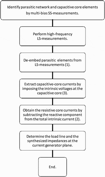
where  represent the matrix of capacitances. Alternatively, a harmonic balance solver can be exploited to obtain the displacement current from the capacitive-core nonlinear model on the trajectory defined by the intrinsic gate and drain voltages. It is worth noticing that, in order to obtain accurate load line estimation at the resistive-core plane, the capacitive-core nonlinear model should also correctly account for non-quasi-static effects, when these effects play a major role. Once this operation has been carried out the resistive core electrical variables are available, which simply allow one to obtain the load line and the synthesized impedances at the current generator at the fundamental and harmonic frequencies. The flowchart reported in Fig. 2 summarizes the fundamental steps of the proposed de-embedding technique.
Flowchart describing the proposed de-embedding technique.

It is worth observing that the approach here proposed does not require any optimization procedure by directly providing the information at the current generators plane starting from the HF large-signal measurements. Moreover, by adopting the proposed procedure, the complex low-frequency dispersion phenomena associated to the current generator [Reference Tasker6, Reference Raffo16, Reference Roh, Kim, Suh, Park and Kim17], which are essentially related to the presence of traps and thermal effects, are automatically accounted for.
III. EXPERIMENTAL RESULTS
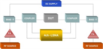
The effectiveness of the procedure outlined in the previous section has been tested on a GaN HEMT (0.7 × 800 µm2). Active LP measurements have been carried out by exploiting an LSNA. A simplified schematic of the employed measurement system is illustrated in Fig. 3. The LSNA provides vector calibrated scattered waves in the 600 MHz–50 GHz harmonic bandwidth. HF sources combined with PAs are used to reproduce realistic trajectories and to actively control the termination at the fundamental frequency. The latter is set equal to 4 GHz and the device is biased at V 0GS = −2 V and V 0DS = 25 V, which corresponds to class-A operation. Different loading trajectories are obtained by varying the phase of the signal injected at the output port thus changing the phase relationship between input and output signals.
Simplified block diagram of the measurement system.

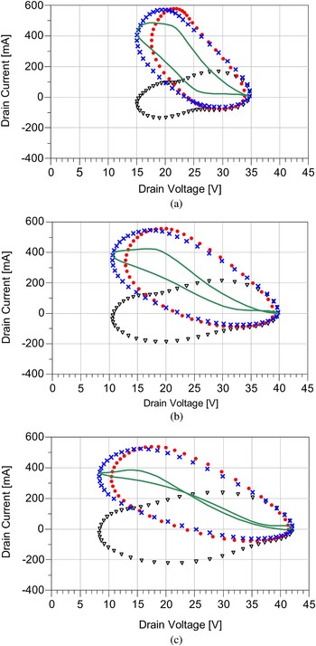
In the present case, the parasitic network was extracted by exploiting a conventional technique based on “cold” scattering parameter measurements, while a quasi-static description was found adequate for the capacitive core. In particular, the bias-dependent capacitances were extracted from multi-bias S-parameter measurements and then stored into a look-up table. Experimental results corresponding to load lines for three different values of the output power are reported in Fig. 4. As observable from the figures, the extrinsic load lines are affected by a strong reactive component whose major contribution is due to the nonlinear capacitive core. In fact, for the selected measurement frequency, the linear parasitic network slightly rotates and shrinks the measured load line as confirmed by comparing the extrinsic load line and the transformed one after applying (1). Finally, in Fig. 4, the load lines at the current generator plane, which actually determine the active device performance and represent the theoretical basis of PA design techniques, are shown. It is clear that the combined effect of the parasitic network in conjunction with the capacitive nonlinearities impacts significantly the shape of the load line masking the information relative to the solely resistive core.
Measured extrinsic load line (dots), load line after parasitic network de-embedding (crosses), displacement current (triangles), and load line at the intrinsic resistive core (continuous line) at: V 0GS = −2 V, V 0DS = 25 V, and f 0 = 4 GHz. Pout = 0.86 W (a); Pout = 1.26 W (b); and Pout = 1.7 W (c).

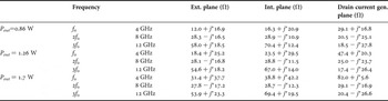
In order to demonstrate the impact of the capacitive core on the impedances synthesized at the current generator plane when microwave operation is involved, in Table 1 a comparison between the synthesized impedances at the three different considered planes (i.e. extrinsic, intrinsic, and current generator planes) is reported. The numbers in the table further highlight the importance of shifting the measurements at the current generator plane where the synthesized impedances strongly differ from the one obtained at the measurement plane. As said, the impedances at the current generator plane determine the voltage and current waveforms which can be compared with the theoretical waveforms in order to perform the so-called waveform engineering [Reference Tasker6].
Load impedances corresponding to the synthesized load lines for three power levels and up to the third harmonic.

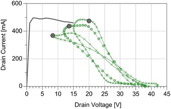
In Fig. 5 the three load lines at the intrinsic resistive core are reported together with the static characteristic measured at V 0GS = 0 V. The marked point on the load lines corresponds to an instantaneous value of the intrinsic gate voltage of 0 V; if low-frequency dispersion was not present these points should belong to the depicted static characteristic. Whereas, as clearly observable, the dynamic I/V significantly deviates from the static characteristics which is the indication of the influence of the thermal effects and the traps [Reference Raffo16, Reference Roh, Kim, Suh, Park and Kim17].
Load lines at the intrinsic resistive core for the output power values reported in Fig. 4 (symbols) and static characteristic at V 0GS = 0 V (continuous line). The marked point on each load line corresponds to the instantaneous gate voltage value equal to 0 V.

It is worth to observe that the proposed technique can be successfully exploited to perform waveform engineering techniques also in the measurement phase by monitoring the dynamic load line at the resistive core while optimum source and loading conditions are achieved at the accessible extrinsic planes.
IV. CONCLUSION
In this work a rigorous approach for the evaluation of the load line at the transistor resistive core under nonlinear HF operation has been formulated. The proposed technique allows one to run-time retrieve from HF large signal measurements the actual load line at the drain–source current generator plane. Consequently, direct information about the dispersive behavior of the I/V nonlinearities are inferred. The proposed approach can be applied to any arbitrary extrinsic load line and exploits a model-based description of the reactive nonlinearities. The latter, together with the parasitic networks, can be identified through standard multi-bias S-parameter measurements.
ACKNOWLEDGEMENTS
This work was supported by the Research Foundation Flanders (FWO-Vlaanderen) and the K.U.Leuven OT project.
 Antonio Raffo was born in Taranto, Italy, in 1976. He received the M.S. degree (with honors) in electronic engineering and the Ph.D. degree in information engineering from the University of Ferrara, Ferrara, Italy, in 2002 and 2006, respectively. Since 2002, he has been with the Engineering Department, University of Ferrara, Italy where he is currently a Research Associate and teaches the courses of Semiconductor Devices and Electronic Instrumentation and Measurement. His research activity is mainly oriented to nonlinear electron device characterization and modeling and circuit-design techniques for nonlinear microwave and millimeter-wave applications. Dr. Raffo is a member of the IEEE MTT-11 Technical Committee.
 Gustavo Avolio was born in Cosenza, Italy, in 1982. He received the M.Sc. degree in electronic engineering from the University of Calabria, Italy, in 2006. In January 2008 he joined the TELEMIC Division of the Katholieke Universiteit of Leuven, Belgium, as a Ph.D. student. His research work focuses on large-signal measurements and nonlinear characterization of advanced microwave devices.
 Dominique M. M.-P. Schreurs received the M.Sc. degree in electronic engineering and the Ph.D. degree at the Katholieke Universiteit Leuven (K.U.Leuven), Belgium. She has been a Visiting Scientist at Agilent Technologies, ETH Zürich and NIST. She is now Associate Professor at K.U.Leuven. Her main research interests concern the (non)linear characterization and modeling of active microwave devices, and (non) linear hybrid and integrated circuit design. D. Schreurs is a member of the INMMiC Steering Committee. She is also serving on the AdCom of the IEEE MTT Society. She is vice-chair of the IEEE MTT-S Technical Coordinating Committee, and past chair of the IEEE MTT-S Technical Committee on microwave measurements. She also serves as education chair on the Executive Committee of the ARFTG organization.
 Sergio Di Falco was born in Licata (AG), Italy, in 1983. He received the M.S. degree in electronic engineering from the University of Ferrara, Ferrara, Italy, in 2008. In 2009 he joined the Engineering Department at the University of Ferrara as a Ph.D. student. His research activity is mainly oriented to nonlinear characterization and modeling of microwave electron devices, HMIC and MMIC design.
 Valeria Vadalà was born in Reggio Calabria, Italy, in 1982. She received the M.S. degree (with honors) in electronic engineering from the “Mediterranea” University of Reggio Calabria, Reggio Calabria, Italy, in 2006 and the Ph.D. degree in information engineering from the University of Ferrara, Ferrara, Italy, in 2010. Dr. Vadalà is currently with the Department of Engineering, University of Ferrara. Her research interests include nonlinear electron-device characterization and modeling for microwave applications.
 Francesco Scappaviva was born in Italy in 1978. He received the laurea degree in electronic engineering in 2004 from the University of Bologna. From 2006 up to now he is with the Department of Electronics, Computer Science and Systems (DEIS – University of Bologna) as Ph.D. Student. In 2004 he joined academic spin-off MEC – Microwave Electronics for Communication – Bologna, Italy, where he works as RF research engineer and his activity is mainly oriented to Hybrid and Monolithic Microwave Integrated Circuit design and characterization. His main research interests are in the field of RF power amplifiers and microwave circuits for space applications and communication systems.
 Giovanni Crupi was born in Lamezia Terme, Italy, in 1978. He received the M.Sc. degree in electronic engineering (cum laude) and the Ph.D. degrees from the University of Messina, Italy, in 2003 and in 2006, respectively. Currently, he is a Contract Researcher with the Dipartimento di Fisica della Materia e Ingegneria Elettronica, University of Messina, where he holds the course of Optoelectronics. Since 2005 he has been a repeat Visiting Scientist with the Katholieke Universiteit (K.U.) Leuven and the Interuniversity Microelectronics Center (IMEC), Leuven, Belgium. His main research interests include small and large signal modeling of advanced microwave devices.
 Bart Nauwelaers was born in Niel, Belgium on 7 July 1958. He received the M.S. and Ph.D. degrees in electrical engineering from the Katholieke Universiteit (K.U.), Leuven, Belgium in 1981 and 1988, respectively. He also holds a Master degree from ENST, Paris, France. Since 1981 he has been with the Department of Electrical Engineering (ESAT) of the K.U.Leuven, where he has been involved in research on microwave antennas, microwave integrated circuits, and MMICs, linear and nonlinear device modeling, MEMS and wireless communications. He is a former chair of IEEE AP/MTT-Benelux and present chair of URSI-Benelux. Bart Nauwelaers teaches courses on microwave engineering, on analog and digital communications, on wireless communications, and on design in electronics and telecommunications. He has been the coordinator of the telecommunications program at the K.U.Leuven and is currently the educational chair for Electrical Engineering at the K.U.Leuven.
 Giorgio Vannini received the Laurea degree in electronic engineering and Ph.D. degree in electronic and computer science engineering, from the University of Bologna, Bologna, Italy, in 1987 and 1992, respectively. In 1993, he joined the Department of Electronics, University of Bologna, as a Research Associate. From 1994 to 1998, he was with the Research Centre on Electronics, Computer science and Telecommunication Engineering, National Research Council (CSITE), Bologna, Italy, where he was responsible for MMIC testing and the Computer-Aided Design (CAD) Laboratory. In 1998, he joined the University of Ferrara, Farrara, Italy, as an Associate Professor, and since 2005, as a Full Professor of electronics. He is currently Head of the Engineering Department. During his academic career, he has been a Teacher of applied electronics, electronics for communications and industrial electronics. He was a cofounder of the academic spin-off Microwave Electronics for Communications (MEC). He has coauthored over 180 papers devoted to electron device modeling, computer-aided design techniques for MMICs, and nonlinear circuit analysis and design. Dr. Vannini is a member of the Gallium Arsenide Application Symposium (GAAS) Association. He was the recipient of the Best Paper Awards presented at the 25th European Microwave Conference, GAAS98 Conference, and GAAS2001 Conference.