I. INTRODUCTION
The development of high-entropy alloy (HEA) has received significant worldwide attention because of the good mechanical propertiesReference Yeh, Chen, Lin, Gan, Chin, Shun, Tsau and Chang1 and corrosion resistanceReference Chen, Duval, Hung, Yeh and Shih2 in the formation of alloys. Yeh et al. introduced the concept of HEA,Reference Yeh, Chen, Lin, Gan, Chin, Shun, Tsau and Chang1 which uses multiprincipal element (at least 5) alloys to replace only one principal element in traditional alloys, such as steel, bronze, and aluminum alloys. In doing so, neither one nor two dominant principal elements affect the properties of HEAs. Surprisingly, HEAs tend to form simple face-centered cubic (FCC) and/or body-centered cubic solid solution phases compared with intermetallic compounds.Reference Yeh, Chen, Gan, Lin, Chin, Shun, Tsau and Chang3 This finding was intuitively attributed to high mixing entropy because thermodynamically speaking, high entropy decreases the Gibbs energy of solid solutions at elevated temperatures to obtain phase selection against intermetallic compounds.Reference Craievich, Weinert, Sanchez and Watson4 The severe lattice distortion caused by the incorporation of multiprincipal elements renders the formation of nanosized and amorphous structures.Reference Takeuchi, Chen, Wada, Yokoyama, Kato, Inoue and Yeh5,Reference Ding and Yao6 HEAs demonstrate enhanced strength combined with good resistance to oxidation and corrosion.Reference Yeh, Chen, Lin, Gan, Chin, Shun, Tsau and Chang1–Reference Yeh, Chen, Gan, Lin, Chin, Shun, Tsau and Chang3 As a result, more researchers have agreed with the HEA concept, thereby promoting further investigation on this field of study.
The alloy and nitride coatings of HEAs have been manufactured as protective coatings via magnetron sputtering system because of their superior physical properties. To increase their hardness, high-entropy nitride coatings with strong nitride-forming elements like AlCrTaTiZrReference Lai, Lin, Yeh and Chang7 and TiVCrZrHfReference Liang, Chang, Tsai, Lin, Sung, Deng and Shieu8 were developed. The nitride coatings not only had increased the hardness of up to 48 GPa but also had only a single NaCl-type phase. Moreover, octonary nitride like AlMoNbSiTaTiVZr nitrideReference Tsai, Lai, Yeh and Gan9 was used to amplify high entropy effects. An alloy design that uses eight target elements is effective in achieving high hardness and thermal stability. Atomic size difference is considered a critical parameter that determines the resultant structure and properties. By virtue of these merits, the AlMoNbSiTaTiVZr nitride coatings exhibited a high hardness of 37 GPa and were verified to be promising diffusion barriers between Cu and Si.Reference Tsai, Wang, Lai, Yeh and Gan10 Even after annealing at 850 °C for 30 min, the nitride coatings sustained amorphous phase and prevented the reaction between Si and Cu.
In the field of hard coatings, transition metal nitrides such as CrN, TaN, TiN, VN, and ZrN have attracted much attention because of their interesting and attractive chemical and physical properties in multifunctional films due to the fact that these films present a high hardness, low friction coefficient, and excellent thermal stability.Reference Pierson11 Among these nitrides, the VN coating was found to show a decrease in the friction coefficient with an increase in temperature due to the formation of V2O5 at a high temperature that make it a suitable compound for high speed machining without lubrication.Reference Gulbiński, Suszko and Pailharey12 The CrN coating was demonstrated to have a high oxidation resistance owing to the formation of a protective Cr2O3 layer.Reference Mayrhofer, Willmann and Mitterer13 Considering various superior properties possessed by different binary coatings, multicomponent systems based on the combination of binary ones are consequently evolved. In our previous study, ternary CrTiV nitride, which had a single FCC crystalline structure that exhibited good mechanical properties, was developed.Reference Tsai, Huang, Lin, Jung, Chang and Shieu14 In this study, larger atomic size difference was designed and realized by alloying with large Zr atoms to suppress crystallization during coating growth. The incorporation of heavy Ta atoms increased significantly the energy of sputtered and backscattered atoms reaching the substrate, leading to densification of coating structure.Reference Abadias, Koutsokeras, Siozios and Patsalas15 These above factors were responsible for the increase of mechanical properties. Thus, it was believed that excellent mechanical properties could be expected in the multicomponent CrTaTiVZr nitrides, so that the five elements Cr, Ta, Ti, V, and Zr were used to manufacture the HEA in this study. Various studies have been performed to understand the relationship between the processing parameters, the coating structure and properties. Since process parameters may differ in different PVD methods, it is difficult to verify the significance of each specific parameter. It is well known that the N2 flow during the coating growth influences some major structure and properties of the coating.Reference Lai, Lin, Yeh and Chang7,Reference Tsai, Lai, Yeh and Gan9,Reference Chang, Huang, Davison, Yeh, Tsau and Yang16–Reference Tsai, Chang, Kuo, Shiao, Chang and Shieu18 Therefore, in this study, the effect of the N2 flow on the structural and mechanical properties of (CrTaTiVZr)Nx coatings deposited on Si substrates via reactive radio frequency sputtering was investigated. The dependence of its structural and mechanical properties such as the film's composition, crystal quality, surface morphology, hardness, and reduced modulus on the N2 flow for (CrTaTiVZr)Nx coatings was discussed.
II. EXPERIMENTAL
The (CrTaTiVZr)Nx coatings were deposited on p-Si (100) wafers via a radio-frequency magnetron sputtering system by using equimolar CrTaTiVZr targets that were 75 mm in diameter. Prior to deposition, the p-Si (100) wafers were cleaned in an ultrasonic bath and then rinsed thoroughly with ethanol and distilled water. They were then placed in the vacuum system. The distance of the target to the substrate was 90 mm, and the deposition angle was 60° relative to the substrate. The center of the target disk was aligned to the middle point between the center and the edge of the substrate holder. The substrate stage was rotated at 5 rpm to obtain homogeneous film quality and thickness. The deposition time was set at 60 min. The sputtering system consisted of a stainless steel vacuum chamber and a turbo pump with a rotary pump, which provided an ultimate vacuum of 2.67 × 10⁻⁴ Pa before introducing the gases. The deposition of the (CrTaTiVZr)N coatings was carried out in an Ar + N2 mixed atmosphere under a RF power of 350 W and a working pressure of 6.67 × 10⁻¹ Pa. During deposition, the Ar flow was controlled at 100 SCCM. The N2 flow was chosen as the controlling parameter, which was varied from 0 to 8 SCCM. The substrate temperature was heated to 450 °C at a rate of 10 K/min and maintained there for 60 min prior to deposition. Then, the substrate temperature and bias were fixed at 450 °C and −100 V during the deposition process, respectively.
The chemical compositions of the (CrTaTiVZr)N coatings were determined via field-emission electron probe microanalyses (FE-EPMA, JEOL JXA-8800M, Japan), and at least three tests were performed for each sample. Quantitative analysis is not accurate for trace and light elements or when significant differences exist between the compositions of the standard (TiN) and the sample. The crystal structures were analyzed using a glancing-incidence (1°) x-ray diffractometer (GIXRD, BRUKER D8 Discover, Germany) with Cu Kα radiation at a scanning speed of 1 deg/min. The scanning step was 0.02°, and the scanning range was 20°–80°. For the pole figure measurements, a step size of 5° for the polar ψ and azimuthal angle ϕ was applied. The residual stress of the films was determined by optical substrate curvature measurements and calculated from Stoney's equation.Reference Larsson, Bromark, Hedenqvist and Hogmark19 Morphology studies and thickness measurements were carried out via field emission scanning electron microscopy (SEM, JEOL JSM-6700F, Japan). The deposition rate was obtained by dividing the thickness from the deposition time. Microstructural examinations were conducted using an analytical transmission electron microscope (TEM, FEI E.O. TecnaiF20, Hillsboro, OR). The hardness and reduced modulus of coatings were measured using a TriboLab nanoindenter (Hysitron Inc.) with a Berkovich diamond indenter tip (tip radius ∼50 nm). During the tests, a maximum applied load of 2000 μN was set. The indentation depth was measured to be about 84, 65, 52, 42, 43, and 44 nm for the coatings deposited at 0, 1, 2, 4, 6, and 8 SCCM, respectively. The detailed methods for measuring the hardness and reduced modulus and for calibrating the tip-area-function were given in Ref. Reference Oliver and Pharr20. Twenty five tests were performed on each sample.
III. RESULTS AND DISCUSSION
A. Deposition rate and chemical composition
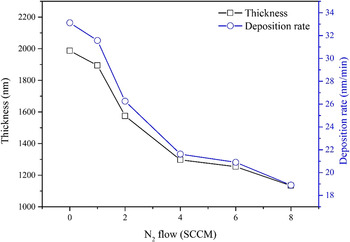
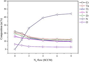
Based on SEM observations (Fig. 6), the coating thickness decreased to 1978, 1894, 1575, 1297, 1254, and 1134 nm as the N2 flow increased from 0, 1, 2, 4, 6, and 8 SCCM, respectively. The deposition rate likewise decreased, as shown in Fig. 1. This occurrence can be attributed to the target poisoning effect and the lower sputtering efficiency of N ions compared with Ar ions.Reference Mason and Pichiling21Figure 2 shows the chemical composition of (CrTaTiVZr)Nx coatings deposited at various N2 flows. The N content in the coatings increased significantly with increasing N2 flow before reaching a value of about 44.2 at.% when the N2 flow was 8 SCCM. Inevitably, the variation in N2 content resulted in a decisive influence on the structures and properties of the formed coatings. Moreover, a slight decrease in the oxygen content in the coatings from 6.2 to 2.7 at.% with R N was observed. The source of oxygen in the coating might be one or both of the following: residual gas and plasma and/or heating-induced desorption from the deposition chamber. The effect of oxygen content on the structures and properties could be ignored given that the oxygen content takes only a very small molar fraction.
Thickness and deposition rate of (CrTaTiVZr)N coatings deposited at different N2 flows.

EPMA element contents in (CrTaTiVZr)N coatings deposited at different N2 flows.

B. Structure analysis
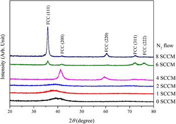
Figure 3 presents the GIXRD patterns of the (CrTaTiVZr)Nx coatings deposited at various N2 flows. When the N2 flow was 0 SCCM, the coatings had a broad peak indicative of an amorphous structure. It has been pointed out that due to the differences in their metallic elements in terms of atomic radius (Cr: 1.249 Å, Ta: 1.430 Å, Ti: 1.462 Å, V: 1.316 Å, and Zr: 1.603 Å.) and structure (Cr, Ta, V: body-centered cubic, Ti and Zr: close-packed hexagonal), the coatings easily developed noncrystalline structures.Reference Lai, Lin, Yeh and Chang7–Reference Tsai, Lai, Yeh and Gan9 On increasing the N2 flow to 2 SCCM, the peak became broader. This indicates an increase of disorderliness of atomic structure. Given that the 26.3 at.% N content of the coatings was not high enough to form a crystalline phase, the dissolved N atoms in the coating were regarded as the sixth alloy element that disturbs the amorphous structure. Thus, a more disordered structure was expected to form. When the N2 flow was increased to 4 SCCM and above, the peaks corresponded to the (111), (200), (220), (311), and (222) planes of a FCC crystal structure were observed. CrN, TaN, TiN, VN, and ZrN all had a FCC phase. The as-deposited mixtures of FCC-forming ternary nitrides, such as ZrTiN,Reference Hasegawa, Kimura and Suzuki22 CrTiN,Reference Hasegawa, Kimura and Suzuki22,Reference Hones, Sanjinés and Lévy23 and CrNbN,Reference Hones, Sanjinés and Lévy23 have been reported as a single FCC solid solution across the entire composition range. As a result, the formation of single FCC solid solution can be expected.
GIXRD pattern of the (CrTaTiVZr)N coatings deposited at different N2 flows.

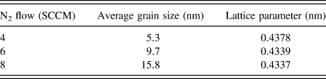
The average grain sizes were calculated based on the Scherrer's formulaReference Klug and Alexander24 using the most intense line of the XRD patterns (Table I),
 $$d = {\lambda \mathord{\left/ {\vphantom {\lambda {\beta \cos \theta }}} \right. \kern-\nulldelimiterspace} {\beta \cos \theta }}\quad ,$$
where d is the average diameter in nm, λ is the x-ray wave length, β is the line broadening at half the maximum intensity in radians, and θ is the Bragg's angle. As the N2 flow increased, the grain size increased from 5.3 to 15.8 nm. This is because more N content would result in fewer vacant N sites, thereby facilitating better grain growth. Moreover, the lower oxygen content at higher N2 flow may be beneficial to grain growth. The lattice parameters derived from the XRD pattern are also given in Table I. The lattice parameter decreased significantly from 0.4378 to 0.4337 nm when the N2 flow was increased from 4 to 8 SCCM. One possible explanation is that the N affinity to Cr is lesser compared with other target elements (ΔH f, CrN = −117.2 kJ; ΔH f, TaN = −252.3 kJ; ΔH f, TiN = −337.7 kJ; ΔH f, VN = −217.2 kJ; ΔH f, ZrN = −365.3 kJ).Reference Dean25 Thus, at a low N2 flow regime, CrN is relatively difficult to form. In other words, the nitride crystallites may contain less Cr element; hence, the lattice parameter is relatively large because CrN has a smaller lattice parameter.Reference Hones, Sanjinés and Lévy23 As the N2 flow increased, the lattice parameter become smaller because the nitride crystallites contain more Cr element.
The average grain size and lattice parameter of (CrTaTiVZr)N coatings.
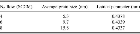
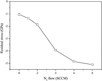
Figure 4 shows the residual stress of the (CrTaTiVZr)N coatings deposited at various N2 flows. It can be seen that the stress becomes increasingly compressive from −1.05 to −5.11 GPa with increasing N2 flow from 0 to 8 SCCM. The result is considered to principally originate from the well-known atomic-peening effect,Reference Kappertz, Drese and Wuttig26 whereby the impinging ions knock surface atoms deeper into the film, where they become trapped. Low sputtering rates were reported to enhance the energetic discharge species to deposit atoms on the growing coatings.Reference Huang and Yeh27 Furthermore, increasing the N2 flow resulted in more low-energy ion fluxes colliding with the growing film.Reference Mahieu, Ghekiere, Winter, Gryse, Depla, Tendeloo and Lebedev28 Both aforementioned factors enhanced the atomic peening effect and thereby increase the compressive stress.Reference Tsai, Huang, Lin, Jung, Chang and Shieu14,Reference Tsai, Chang, Kuo, Shiao, Chang and Shieu29
The residual stress of the (CrTaTiVZr)N coatings deposited at different N2 flows.

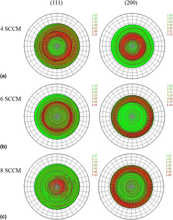
The N2 flow has a strong influence on the preferred orientation of (CrTaTiVZr)Nx coatings. The coatings deposited at a N2 flow of 8 SCCM exhibited a very strong (111) preferred orientation. To deeply examine the structural properties of (CrTaTiVZr)Nx coatings, the statistical distribution of the (111) and (200) planes as a function of the polar ψ and azimuthal ϕ coordinates is presented in Fig. 5 by using pole figures. The results indicate a preferred crystallite orientation in the form of strong fiber textures for all coatings. At a N2 flow of 4 SCCM [Fig. 5(a)], the (200) pole figure exhibits a strong ring at a diffraction angle of ψ = 26°. By contrast, the (111) pole figure reveals weak and broad reflections in a ring pattern at ψ = 37°. This result implies that the coating has a slight (200) preferred orientation. When the N2 flow was further increased to 6 SCCM [Fig. 5(b)], the (111) pole figure features a sharp diffracted ring pattern at ψ = 35°, whereas the (200) pole figure displays a more broadened diffracted ring pattern at ψ = 48°. When the N2 flow reached 8 SCCM [Fig. 5(c)], the (111) pole figure shows a (111) texture with the majority of intensity maxima concentrated at the center of the pole. The (200) pole figure is characterized by a ring-type intensity pattern at ψ = 48°. Therefore, a (111) preferred orientation evolves with increasing N2 flow. The preferred orientation is a consequence of the competition between neighboring grains. As the N2 flow increased, the competition growth became more significant because of a few vacant N sites. For materials with a [NaCl-type (β1)] FCC phase, the diffusion of adatoms on the low-energy (002) plane is easy because this plane offers the lowest number of nearest neighbors to the incoming adatom, whereas the diffusion on the (111) plane is much more difficult because of the highest number of nearest interacting neighbors. The diffusing adatoms on the (200) plane may migrate to the edges. As such, their incorporation on the lattice sites of the adjacent (111) grains becomes highly probable. As a result, the preferred orientation of the coatings evolved toward the (111) orientation.
Pole figures from (111) and (200) reflections of (CrTaTiVZr)N coating films deposited at different N2 flows. (a) 4, (b) 6, and (c) 8.

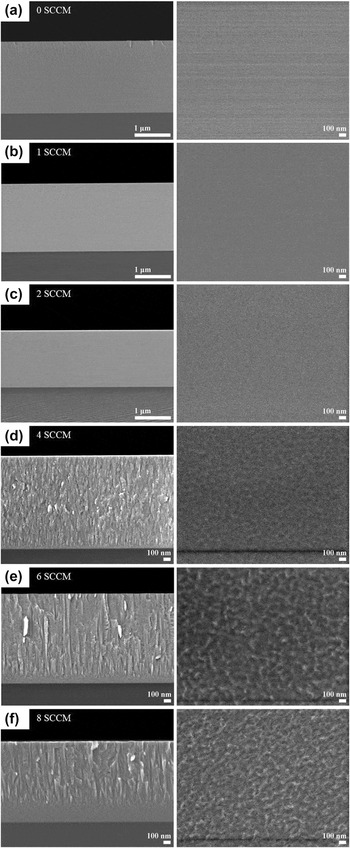
Figure 6 shows the SEM micrograph of (CrTaTiVZr)Nx coatings deposited at various N2 flows. The coatings deposited at N2 flows of ≤2 SCCM had a very smooth morphology without any special feature, which is typical for an amorphous structure. When the N2 flow was increased to 4 SCCM, the coatings exhibited a fibrous structure with a slightly rough surface. When the N2 flow was further increased to 6 SCCM and higher, the structure was transformed into a columnar type with increased column width. Two distinct layers separated by a boundary were observed. The underlayer has a smooth morphology without any special feature, whereas the upper layer had a columnar structure. To verify the structural evolution during coating growth, TEM characterizations were performed to achieve a more detailed evaluation of the microstructure.
SEM micrographs of the (CrTaTiVZr)N coatings deposited at different N2 flows: (a) 0, (b) 1, (c) 2, (d) 4, (e) 6, and (f) 8.

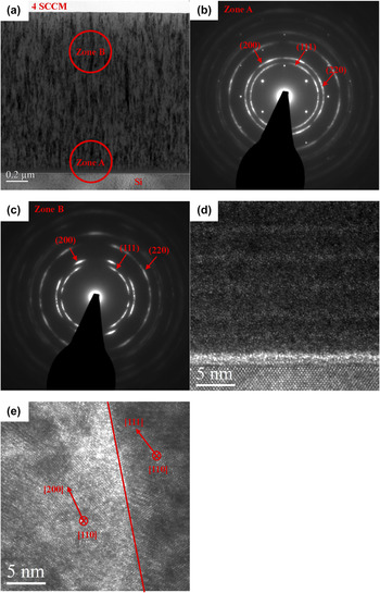
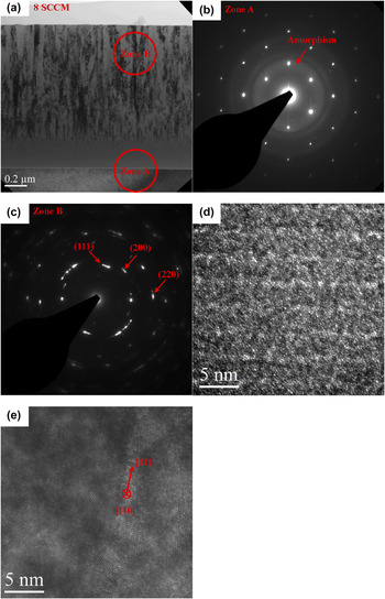
Figure 7 shows the TEM images with the selected area diffraction (SAD) pattern of (CrTaTiVZr)Nx coatings deposited at a N2 flow of 4 SCCM. The structure of the coating had two distinct layers [Fig. 7(a)]. The upper layer had a fibrous microstructure with the fiber widths of 20–30 nm. The lower layer shows an amorphous structure of approximately 15 nm thick. Two SAD patterns of equal size were labeled as Zone A and Zone B. Zone A exhibited diffraction rings that correspond to the (111), (200), (220), and (311) planes of the FCC phase [Fig. 7(b)]. Zone B contains arc-like FCC diffraction rings [Fig. 7(c)], which indicates the existence of a slight (200) preferred orientation. High resolution TEM (HRTEM) observations [Figs. 7(d) and 7(e)] further demonstrated that the underlayer had an amorphous phase, whereas the upper layer is composed of (111)- and (200)-oriented FCC grains. Based on these aforementioned analyses, the structural evolution of coating thickness can be concluded. The coating was initially formed as a continuous 15 nm-thick amorphous layer. As the coating grew, nucleation of randomly oriented grain occurred from the amorphous layer. Afterward, tapered crystallite with FCC phases began to develop and induced competition between neighboring grains. This competition led to an evolutionary selection of the fastest-growing grains.Reference van der Drift30 However, the coating is only slightly favored by the (200) preferred orientation, which may be ascribed to limited grain growth. Figure 8 shows the TEM images with the SAD pattern of (CrTaTiVZr)Nx coatings deposited at a N2 flow of 8 SCCM. The coating still exhibited two distinct layers [Fig. 8(a)]. However, the column width increased to approximately 30–50 nm. Meanwhile, the amorphous underlayer on the substrate thickened to about 135 nm. Based on the SAD and lattice images [Figs. 8(c) and 8(f)], the columnar structure revealed a strong (111) preferred orientation. These phenomena have been discussed previously.
Cross-sectional TEM micrographs of the (CrTaTiVZr)N coatings deposited at a N2 flow of 4 SCCM. (a) Bright-field image. (b) SAD patterns of Zone A. (c) SAD patterns of Zone B. (d) HRTEM lattice image of the bottom part of the cross-section. (e) HRTEM lattice image of the top part of the cross-section.

Cross-sectional TEM micrographs of the (CrTaTiVZr)N coatings deposited at a N2 flow of 8 SCCM. (a) Bright-field image. (b) SAD patterns of Zone A. (c) SAD patterns of Zone B. (d) HRTEM lattice image of the bottom part of the cross-section. (e) HRTEM lattice image of the top part of the cross-section.

From the SEM and TEM observations, it is interesting that the thickness of the amorphous layer increased with increasing N2 flow. Hu et al. demonstrated that stress induced the formation of the amorphous layer, which indicated that the formation of the amorphous layer is a form of stress relaxation.Reference Hu, Kong, Wang, Wan and Duan31 Song et al. proposed that the amorphous layer thickness is dependent on process parameters, such as sputtering power, N2 partial pressure, substrate temperature, and substrate bias.Reference Song, Wang, Sung, Huang and Lii32 In the present study, the deposition was under tremendous compressive stress, thereby preventing the formation of the crystalline phase.Reference Kim and Jin33,Reference Tsai, Chang, Kuo, Lin, Lin and Shieu34 As mentioned, increasing the N2 flow enhances the atomic peening effect and decreases the amount of ductile amorphous metal for stress relaxation, thereby leading to high compressive stress. As a result, the increase in amorphous layer thickness is expected. This unusual transition in the microstructure has been seldom reported in other nitride coating systems. The determination of the multiprincipal components may be an important issue for the expansion of the amorphous interlayer. Noticeably, layering structure in the coatings was found in the TEM images [Figs. 7(d) and 8(d)]. This observation can be attributed to the deposition conditions used in this study. The layer thickness was associated with the rotation speeds of the substrate.
C. Mechanical properties
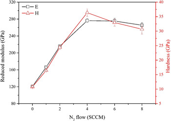
Figure 9 displays the hardness and reduced modulus of (CrTaTiVZr)Nx coatings as functions of N2 flow. For the alloy coating, the hardness and modulus were 10.8 and 120.8 GPa, respectively. The higher hardness of CrTaTiVZr alloy coatings than those of typical coatings of pure metals and alloys was attributed to the strong interaction between atomic pairs and the amorphous structure, which contains no dislocations for slip. When the N2 flow was increased to 4 SCCM, the hardness also continued to increase and reached a maximum value of 36.4 GPa. The enhanced hardness is attributed to the increased N content, which indicates a high amount of strong Me–N bonding in the coatings. By further increasing the N2 flow to 8 SCCM, the hardness significantly decreased to 30.7 GPa. The larger grain size is considered as the main factor according to the Hall–Petch effect.Reference Veprek35 It is well known that grain boundaries impede dislocation movement and that the number of dislocations within a grain have an effect on how easily dislocations can traverse grain boundaries and travel from grain to grain. So, by changing the grain size, one can influence the dislocation movement and mechanical property, which is typical for Hall–Petch effect. In the present study, the reduced modulus of the coating exhibited the same trend as hardness. This finding was due to an intense pressure experienced by the material in the indenter during the hardness and modulus measurements. At a fixed applied load, a higher material hardness caused smaller projected area of the remaining indentation and higher average pressure in the indenter. Therefore, high hardness resulted in high values of the measured reduced modulus.Reference Veprek and Argon36
Hardness and reduced modulus of the (CrTaTiVZr)N coatings deposited at different N2 flows.

IV. CONCLUSION
The microstructural and mechanical properties of (CrTaTiVZr)Nx coatings deposited on an Si substrate via reactive radio-frequency magnetron sputtering as a function of N2 flow were investigated. The N content increased rapidly at low N2 flows and reached about 44.2 at.% when the N2 flow was at 8 SCCM. At low N2 flows (≤2 SCCM), the structure of the coatings was amorphous with featureless morphology because of deficient N content. At a N2 flow of 4 SCCM, a fiber structure with a FCC phase (200) preferred orientation was observed. Moreover, a 15 nm-thick amorphous layer was formed near the substrate. When the N2 flow was increased to 8 SCCM, the microstructure obviously changed to a columnar structure with large grain size because of decreased N vacancy. However, the amorphous structure thickened to about 135 nm. The transformation of unusual microstructure was attributed to the enhanced atomic peening effect at high N2 flows. The (111) orientation is preferred because the (111) plane exhibited low strain energy. The hardness of the coating attained a maximum of 36.4 GPa when deposited at a N2 flow of 4 SCCM. This attributed to a high amount of strong Me–N bonding and small grain size (∼5 nm). The present alloy design is effective and may have high potential in hard coating applications after further research and development.
ACKNOWLEDGMENT
The authors gratefully acknowledge the financial support for this research by the Ministry of Science and Technology of Taiwan under Grant No. 103-2622-E-167-011-CC3.