Introduction
The development of the ubiquitous information technology (IT) industry has been driven by Moore’s law on transistor scaling, the exponential increase in complementary metal oxide semiconductor (CMOS) transistor density on a chip with time. Also key to performance improvement is the associated increase in clock speed, enabled by a systematic reduction in voltage with time (Dennard or classical scalingReference Baccarani, Wordeman and Dennard1). The voltage reduction concomitant with the speed increase is vital, as otherwise increased speed would result in increases in power and hence in unacceptable heat production. After 2003, the voltage could no longer be lowered below about 1 V because a fundamental physical limit of the CMOS transistor had been reachedReference Haensch, Nowak, Dennard, Solomon, Bryant, Dokumaci, Kumar, Wang, Johnson and Fischetti2 that then stalled further increases in speed. The fundamental limit on voltage arises from the need to turn the device off by applying an electrostatic potential to the channel, creating a statistical-mechanical barrier that single carriers (electrons/holes) find hard to cross.Reference Haensch, Nowak, Dennard, Solomon, Bryant, Dokumaci, Kumar, Wang, Johnson and Fischetti2 The barrier height cannot be larger than the electronic charge e times line voltage V DD, while the temperature T sets a scale k BT for the carrier energy, where k B is the Boltzmann constant. Since eV DD/k BT must not fall below a certain value for effective switch-off, there is a floor under the line voltage value at room temperature. Engineering and materials science innovation applied to CMOS cannot overcome its fundamental physical limitation, and hence the only route to restore scaling is the development of a conceptually novel low voltage/low power and high frequency device.Reference Theis and Solomon3 If developed and implemented successfully, the new device could reinvigorate the IT industry.
Approaches toward developing an alternative computer switch concept have been reviewed by Theis and Solomon.Reference Theis and Solomon3, Reference Theis and Solomon4 They included “energy filtering,” as exemplified by the tunnel field-effect transistor (FET),Reference Banerjee, Richardson, Coleman and Chatterjee5 “internal potential step-up,” as illustrated by the ferroelectric-gate FETReference Salahuddin and Datta6 and quantum capacitive devices,Reference Kopp and Mannhart7 and “internal transduction.” Among the latter are the spin-FETReference Datta and Das8 and nano-electromechanical switch.Reference Buettiker, Imry, Landauer and Pinhas9 However, none of the present embodiments of the mentioned concepts has been demonstrated to perform at a level that would make it competitive with the FET as device scales are further reduced.
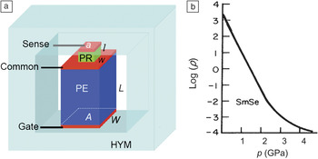
In response to this challenge, a new device concept, the piezoelectronic transistor (PET) has been put forward (see Figure 1a). Simulations of the PET design, described later, show that it can indeed meet the challenge of operability at low voltages and higher speeds than conventional CMOS. The PET functions by transducing an electrical gate signal into acoustic form via a high performance relaxor piezoelectric (PE) element.Reference Park and Shrout10–Reference Baek, Park, Kim, Aksyuk, Das, Bu, Felker, Lettieri, Vaithyanathan, Bharadwaja, Bassiri-Gharb, Chen, Sun, Folkman, Jang, Kreft, Streiffer, Ramesh, Pan, Trolier-McKinstry, Schlom, Rzchowski, Blick and Eom12 The acoustic signal then compresses a rare-earth chalcogenide intermediate valence piezoresistive (PR) element, which undergoes an insulator-to-metal transition driven by f-electron physics.Reference Jayaraman, Narayanamurti, Bucher and Maines13, Reference Jayaraman and Maines14 The insulator-to-metal transition makes the channel (sense-common path—see next section) of the device conductive and transduces the acoustic signal back to electrical form. This transduction mechanism circumvents the direct electrostatic gating principle of CMOS FETs, allowing lower voltage operation to be supported.Reference Newns, Elmegreen, Liu and Martyna15 Based on measured properties of known bulk materials, PET devices are predicted by theory and simulation to support Dennard-like constant field voltage-scaling, with line voltage a factor of 10 below the roughly 1 V limit of the CMOS FET, while consuming 1/100ththe power of a comparable FET.Reference Newns, Elmegreen, Liu and Martyna16
The piezoelectronic transistor and components. (a) The piezoelectronic transistor (PET)Reference Newns, Elmegreen, Liu and Martyna15, Reference Newns, Elmegreen, Liu and Martyna16 showing gate, common, and sense contacts, and the piezoelectric (PE) and piezoresistive (PR) elements. The device is surrounded by a mechanical clamping structure fabricated from a high yield material (HYM—semitransparent, light blue). Typical dimensions for a post-complementary metal oxide semiconductor device would be {l = 2 nm, w = 4 nm, W = 20 nm, L = 26 nm}. (b) Piezoresistive response of the SmSe PR material,Reference Jayaraman, Narayanamurti, Bucher and Maines13 showing an exponential drop of resistance (ρ) under pressure (p) until metallization occurs at 3.5–4 GPa. Note: l, thickness of piezoresistor; w, width of piezoresistor; a, area of piezoresistor; L, thickness of piezoelectric; W, width of piezoelectric; A, area of piezoelectric.

Here, we review the PET device, describe the relationship between its structure and function, and discuss the key role played by the piezoresistive and PE materials in its performance.Reference Newns, Elmegreen, Liu and Martyna15 We then present the results of theory and simulation of simple PETReference Newns, Elmegreen, Liu and Martyna16 circuits, which suggest that this can indeed supply the low voltage/low power and high speed demanded by post-CMOS computer architecture. This finding strongly motivates experimental development of the PET. The PET concept can be thought of as a general class of devices wherein piezoelectric actuators drive piezoresistive elements, suggesting it could be extended further.
The piezoelectronic transistor
We review the basic principles underlying the PET, the physics of the materials that enable its operation, and then present predictions of PET performance from simulation and modeling based on bulk material properties.Reference Newns, Elmegreen, Liu and Martyna15, Reference Newns, Elmegreen, Liu and Martyna16
Principles of PET operation
The PET is sketched in Figure 1a.Reference Newns, Elmegreen, Liu and Martyna15, Reference Newns, Elmegreen, Liu and Martyna16 The essentials of the structure consist of a stack of two distinct materials: the PE and the PR sandwiched between three contacts: the gate, common, and sense. The PE is located between the gate and common contacts, and the PR between the common and sense contacts. Electrically, the gate can be thought of as the device input, and the sense as the output.
When an input signal is placed on the gate, a voltage is applied across the PE. During manufacture, the PE is “poled” (i.e., given a permanent polarization direction so that the applied voltage expands it along the vertical axis). Expansion of the PE element results in compression of the adjacent piezoresistive element. For this to occur, the whole PET stack needs to be vertically clamped within a rigid structure made of a high yield material (HYM), sketched in semi-transparent form in Figure 1a. The piezoresistive material being compressed has a strongly pressure-dependent resistivity, as shown by the example of SmSe in Figure 1b, where the resistivity changes by almost 7 orders of magnitude for up to ~4 GPa of pressure, from a highly resistive semiconductor down to a low value found in some metallic alloys.Reference Jayaraman, Narayanamurti, Bucher and Maines13, Reference Jayaraman and Maines14 Hence the application of pressure can make the “channel” of the material, between the common and sense contacts, conducting, turning on the device. The net effect is that the input voltage, applied across the capacitor-like input between gate and common, can turn on the path between the common and sense contacts.
The geometry of the PET structure is designed to optimize its function both mechanically and electrically. The area, A, of the PE is made larger than the area, a, of the PR (the areas a and A are shown in Figure 1a) to enhance the pressure in the latter (“hammer and nail” principle). This also reduces the necessary pressure in the PE, which avoids pressure-induced depoling. The aspect ratio of the PE is pillar-like (see Figure 1a) to reduce the clamping (motional constraint in the horizontal plane) by its substrate—clamping lowers the effective PE response.
The aspect ratio of the PR is plate-like (see Figure 1a), its thickness vertically being less than its width. This facilitates transmission of current in the vertical direction, lowering the electrical resistance. This is important for device speed. The small thickness of the PR relative to that of the PE enhances strain in the PR and hence also increases the pressure there.
In absolute terms, the thickness of the PE is only tens of nanometers at scale. So the pressure pulse initiated by applying a sharp electric voltage pulse to the gate is rapidly transmitted across the device. To estimate this time, if we assume a PE thickness of 20 nm and a sound velocity of 4000 m/s, the acoustic transmission time or “sonic time” would then be 5 ps.Reference Newns, Elmegreen, Liu and Martyna15, Reference Newns, Elmegreen, Liu and Martyna16 This is an acceptably short time corresponding to a computer clock frequency on the order of 10 GHz—much faster than current computer clock speeds.
Basic PET equations
An approximate static analysis of PET behavior, illustrating the geometrical effects just described, can be done within an effective one-dimensional approximation.Reference Newns, Elmegreen, Liu and Martyna16 Key equations are
 $${\rm{\mu }} = - \left({1/2} \right)\ln \left({r_{{\rm{ON/OFF}}} } \right),$$
 $$r_{{\rm{ON/OFF}}} = e^{ - V_{{\rm{DD}}} /V_{\rm{\theta }} } <italic>, and </italic>$$
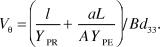 $$V_{\rm{\theta }} = \left({{l \over {Y_{{\rm{PR}}} }} + {{aL} \over {AY_{{\rm{PE}}} }}} \right)/Bd_{33}$$
.
Here μ is the device voltage gain, r ON/OFF is the ratio between the ON and OFF electrical resistance, V DD is the operating line voltage, and V θ is an intrinsic switching voltage threshold. The dimensions l and L and the areas a and A are shown in Figure 1a. Y PR and Y PE are the Young’s moduli of the PR and PE, respectively, B is the slope  $ - \partial \ln \left({\rm{\rho }} \right)/\partial p$ of the resistivity/pressure plot in Figure 1b, and d 33is the PE sensitivity coefficient (matrix notation is used to describe the anisotropic PE response: the induced polarization and strain are both parallel to the direction of the remanent polarization in the PE).
For purposes of engineering a high fidelity device, an ON/OFF ratio r ON/OFF = 10-4 is adequate, giving a gain of μ = 4.6 from Equation 1, which is also an adequate gain for circuit operation. Equations 2 and 3 specify what is needed to get this ON/OFF ratio. From Equation 2, we see that for an (extremely low) operating line voltage, V DD = 0.15 V, we need approximately V θ = 0.016 V. The threshold voltage must be quite low; for this we turn to Equation 3. We see that a low threshold voltage is favored by a large slope in Figure 1b, for the resistivity/pressure curve, and by a large PE sensitivity. The other factors involve PET geometry and mechanical properties of the materials. If the Young’s moduli are both 100 GPa, L = 40 nm, l = 5 nm, and the area ratio A/a = 10.0; then we need a PE d 33 of 1.0 nm/V. Values of d 33 = 2.5 nm/V have been achieved in PMN-PT (Pb[Mg1/3Nb2/3]O3–PbTiO3) single crystals,Reference Li, Zhang, Xu, Wei, Luo and Shrout11 but d 33= 1.0 nm/V is still aggressive for a thin film. Evidently, materials optimization will be needed for PETs to reach the extreme low-voltage goals desired by the electrical engineering community.
The PET is expected to be a fast device for two reasons. First, the sound propagation time is short on the nanoscale. In the previous example, L = 40 nm for a sound velocity of 4000 m/s, and the delay is 10 ps. Second, the pressure mechanism used in the PET is able to gate a metal: the PR can be metalized to resistances as low as a few tens of ohms. This makes the electrical engineering resistance-capacitance (RC) time constants for the PET output to charge the gate of another PET potentially extremely small. Simulations described later show that indeed very short inter-stage logic delays can be achieved by using PET logic.
Hence simple analysis shows that the PET is a device with an adequate ON/OFF ratio, significant gain, and device switching time (both sound transmission time and RC time constant) intrinsically very short. These are very promising characteristics; however, they depend on achieving excellence in material properties.
High response piezoelectric and piezoresistive materials and potential for scaling
Reference 15 describes in detail the materials of interest for the PET. These include relaxor piezoelectricsReference Park and Shrout10, Reference Li, Zhang, Xu, Wei, Luo and Shrout11 discovered in the 1990s and rare-earth intermediate valence chalcogenide compounds such as SmSe and SmxEu1–xS studied extensively in the 1970s and 1980s.Reference Jayaraman, Narayanamurti, Bucher and Maines13, Reference Jayaraman and Maines14 We summarize the mechanism underlying the behavior of these materials, their role in optimizing PET performance, and the prospects for scaling these materials down to the nanoscale.
Relaxor-based PEs such as PMN-PT (Pb[Mg1/3Nb2/3](1–y)O3–PbTiyO3) are known for their high PE response coefficients, d 33, approximately 5–10 times larger than those of standard materials such as PZTReference Park and Shrout10, Reference Li, Zhang, Xu, Wei, Luo and Shrout11 (Pb[ZrxTi1–x]O3). Their mechanism has been discussed in the framework of a Landau-Devonshire free-energy functional by Iwata et al.Reference Iwata, Orihara and Ishibashi17 and by Damjanovic et al.Reference Davis, Budimir, Damjanovic and Setter18 These materials, such as PMN-PT, are intrinsically cubic perovskites, with a lattice distortion induced by the ferroelectric polarization; for example, if the polarization lies along (111), the crystal is rhombohedral, or if along (001), it is tetragonal. As a function of composition y, PMN-PT is rhombohedral for low y and tetragonal for large y, while there is an intermediate transitional region around the PMN-PT stoichiometric parameter y = 0.33, termed the morphotropic phase boundary (MPB), where several symmetries coexist. At the MPB, polarization rotation is facile. For a rhombohedral composition, y < 0.33, the polarization is poled so as to be along a combination of one of the four directions (±1, ±1,1). The polarization can be rotated toward the z-axis (0,0,1) by an electric field E along the z direction (0,0,E). This distorts the crystal in a manner proportional to E, giving rise to the PE effect. When the composition y is close to the MPB but still in the rhombohedral phase, the rotation by the field E is very easy, giving a large PE coefficient d 33. This effect is coupled to other properties,Reference Iwata, Orihara and Ishibashi17, Reference Davis, Budimir, Damjanovic and Setter18 such as the elastic moduli and dielectric constant, which also exhibit anomalies near the MPB.
Both in the bulkReference Park and Shrout10, Reference Li, Zhang, Xu, Wei, Luo and Shrout11 and thin-film forms,Reference Baek, Park, Kim, Aksyuk, Das, Bu, Felker, Lettieri, Vaithyanathan, Bharadwaja, Bassiri-Gharb, Chen, Sun, Folkman, Jang, Kreft, Streiffer, Ramesh, Pan, Trolier-McKinstry, Schlom, Rzchowski, Blick and Eom12 relaxors have been shown to support large strains and survive large applied fields (compared to PZT). Regarding the potential for scaling down to the nanoscale, we note the novel work described in Reference 12 on PMN-PT thin films and that in Reference 19, which shows that ferroelectric behavior in PbTiO3 is present down to nearly the Angstrom scale. Lastly, PE materials are known to survive repeated cycling on the macroscale.Reference Kholkin, Colla, Tagantsev, Taylor and Setter20 Although scaling of this property to the nanoscale has not been studied, it seems reasonable to expect it to continue, as nanoscale materials often exhibit remarkable toughness.
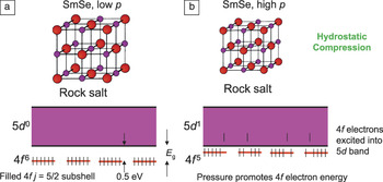
The high piezoresistive response of rare-earth intermediate valence chalcogenide compoundsReference Jayaraman, Narayanamurti, Bucher and Maines13, Reference Jayaraman and Maines14 such as SmSe and SmxEu1–xS arises as follows (see Figure 2a). In these materials, there is an empty 5d conduction band, an occupied 4p valence band, and in the bandgap a narrow, occupied, 4f band derived from the j = 5/2 4f subshell. Under pressure (see Figure 2b), the energy gap E g between the filled 4f band and the empty 5d conduction band narrows, allowing the 4f electrons to be thermally promoted into the 5d conduction band. If the gap narrows linearly with pressure, then there is an exponentially increasing concentration of 5d carriers with pressure, explaining the exponential resistivity/pressure curve in Figure 1b. At high enough pressure, most of the 4f electrons have been promoted into the 5d band, and the system becomes a metal, with no further increases in conductivity (see the foot in resistivity at p = 3.5–4 GPa in Figure 1b). This pressure-induced insulator-to-metal transition occurs at constant space group (rock salt structure) of the material and is reversible with insignificant hysteresis.Reference Jayaraman, Narayanamurti, Bucher and Maines13, Reference Jayaraman and Maines14 It is expected that the 4f electrons will inject on the femtosecond time scale from bandwidth considerations (e.g., much faster than the time scale for the PR lattice contraction, which is on the order of picoseconds). As rock salt is a simple structure and the mechanism of the metal-insulator transition is not complex (electrons are simply ‘‘squeezed out’’ of the 4f-band into the conduction d-band) and essentially local on the atomic scale, prospects are good for piezoresistive property scaling to small dimensions, as described later. The isostructural nature of the transition bodes well for reproducible, repeated cycling in a device.
Functional mechanism of the piezoresistive material.Reference Jayaraman, Narayanamurti, Bucher and Maines13, Reference Jayaraman and Maines14 (a) Top, rock salt lattice of SmSe. Bottom, band structure of SmSe showing filled j = 5/2 4f sub-band in gap, and empty 5d conduction band; E g denotes the bandgap between 4f and 5d bands. Note: purple atoms = Sm; red atoms = Se. (b) Top, SmSe lattice under isostructural compression. Bottom, effect of pressure p on bands. 4f band moves close to the bottom of the 5d band, enabling promotion of 4f electrons into the conduction band, allowing the system to become an electrical conductor.

Last, we have shown elsewhere that by assuming piezoresistive and PE bulk materials properties scale appropriately,Reference Newns, Elmegreen, Liu and Martyna15 the PET device possesses its own analogue of Dennard scaling.Reference Newns, Elmegreen, Liu and Martyna16 We, therefore, next investigate PET speed and performance through simulation and modeling using bulk material properties.
Complementary PET devices
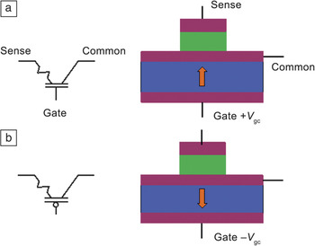
The standard computer logic CMOS involves complementary pairs of transistors, which are turned on by the opposite sign of gate voltage. The advantages include the absence of the need for auxiliary resistors and the fact that logic circuits draw current and dissipate power only during switching—the circuits can have very low standby currents. With PETs, very similar logic circuit families to CMOS with the same advantages can be designed around the concept of complementary PETs. In one approach, the complementary PET is exactly the same as the PET shown in Figure 1a except that the poling direction of the PE is reversed, and it is hence activated by negative gate voltage (see Figure 3). An alternative way to build complementary PETs uses the concept of the 4-terminal PET.Reference Elmegreen, Martyna, Newns and Solomon21
Complementary piezoelectronic transistors (PETs) for piezotronic logic.Reference Newns, Elmegreen, Liu and Martyna15, Reference Newns, Elmegreen, Liu and Martyna16 The piezoelectric in a PET may be poled in two opposite directions (blue piezoelectric, green piezoresistor); the orange arrow shows the polarization direction; purple areas are the contacts labeled sense, common, and gate. (a) Illustration shows poling sense for a positive voltage V gc (gate-common voltage drop) to expand the piezoelectric and compress the piezoresistor. (b) Illustration shows poling sense for a negative voltage V gcto expand the piezoelectric and compress the piezoresistor. These choices form noninverting and inverting PETs, respectively. The corresponding circuit symbols are illustrated at left; conventionally a bubble at the input signifies inversion.

It is axiomatic that inverters and NAND (Not And) gates are sufficient to comprise all logic operations. Piezotronic logic provides complementary inverters (see below) and NAND gates, hence it follows that PETs and complementary PETs are sufficient to construct all CMOS logic gates as well as some useful gates that do not exist in CMOS.Reference Newns, Elmegreen, Liu and Martyna16 We have also demonstrated through theory and simulation that PETs possess non-trivial gain (see Equation 1) that allows them to function in circuits.Reference Newns, Elmegreen, Liu and Martyna15, Reference Newns, Elmegreen, Liu and Martyna16
Simulation and modeling of PET performance
We have modeled complementary PET circuits as described in Reference 16. In order to study the dynamical response of PET logic gates, we developed an electro-acoustic modeling approach to treat complementary PET circuits.Reference Newns, Elmegreen, Liu and Martyna16, Reference Landau and Lifschitz22–Reference Chen24 Briefly, to summarize the elements of the simulation: (1) The PR is treated within linear elasticity theory,Reference Landau and Lifschitz22 and the PE with the standard equations of linear piezoelectricity,Reference Tiersten23, Reference Chen24 with bulk materials properties taken from References 25 and 26. (2) The time evolution of the charge density on the two PE surfaces is coupled to the system via the gate-common current. (3) The variable resistance of the PR is assumed to respond adiabatically to the internal stress generated by PE motion. (4) The HYM is replaced by a “perfect clamp” boundary condition such that L+1 (see Figure 1a) is constant, a good approximation as the HYM is both thick and built from a stiff material such as silicon nitride. (5) The capacitance of each individual PET in a circuit is treated explicitly (due to the high permittivity of piezoelectrics, the capacitance of a PET is dominantly the internal gate capacitance—external parasitic capacitances are relatively small).
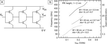
A very simple piezotronic logic circuit is the inverter; Figure 4a shows a chain of three inverters.Reference Newns, Elmegreen, Liu and Martyna15, Reference Newns, Elmegreen, Liu and Martyna16 The inverter consists of two complementary PETs (see Figure 3) in series with the gates joined to form the input. Under static conditions, one of the two PETs is always off, so no standby current is drawn. With the input low (at ground, zero, potential), the lower PET is off, the upper PET on, then the output is high (at the line voltage V DD). With the input high, the upper PET is off, the lower PET is on, and the output is low. Changing the input from low to high changes the output from high to low.
Modeling and simulation of a piezoelectronic transistor (PET) inverter chain.Reference Newns, Elmegreen, Liu and Martyna15, Reference Newns, Elmegreen, Liu and Martyna16 (a) A chain of PET inverters. The complementary PET is denoted by the bubble next to the bars denoting the PE (shown as a capacitor). (b) Simulation of PET performance at scale, frequency scale (left scale) shows inverse switching time in a chain of 9 inverters for PETs of selected geometries; clock speed (right scale) is based on 15 logic steps per clock cycle. Horizontal scale is line voltage (V DD). Device dimensions as per Figure 1a. Note: V in, input voltage ; V out, output voltage; 0, 0 V on the ground line in the circuit; A, area of the piezoelectric; a, area of the piezoresistor; L, thickness of the piezoelectric; l, thickness of the piezoresistor; W, width of the piezoelectric; w, width of the piezoresistor; PR, piezoresistor. The results show multi-GHz performance at low voltage.

In Figure 4b,Reference Newns, Elmegreen, Liu and Martyna15, Reference Newns, Elmegreen, Liu and Martyna16 we show the results of the simulation of a chain of nine PET inverters. For each geometry, lower voltage operation leads to lower operating frequency, f (as in CMOS). However, at line voltages between 0.1 V and 0.2 V, PETs are capable of sustaining multi-GHz clock speeds—this is not achievable with CMOS, where line voltages V DDbelow about 1 V lead to a dramatic slowing down/an inadequate ON/OFF ratio. The signal transduction into acoustic form has paid off in lifting the operational voltage constraint that has kept CMOS clock speeds frozen for a decade.
The power (P = CV DD2f) depends on capacitance C. Estimates show that PET capacitances are similar to capacitances of comparable CMOS logic devices.Reference Newns, Elmegreen, Liu and Martyna15, Reference Newns, Elmegreen, Liu and Martyna16 Hence at V DD = 0.1 V, power will be reduced by 100x relative to CMOS at the same operating frequencies, f. These simulations show that satisfaction of the desired engineering goal of low power combined with high speed by piezotronics is within sight.
Summary and conclusion
The challenge to the information technology (IT) industry posed by the end of complementary metal oxide semiconductor (CMOS) voltage scaling in 2003, resulting in freezing of processor clock speed, can only be met by a computer switching device based on a novel principle.Reference Theis and Solomon3 The piezoelectronic transistor (PET) computer switch that we have proposed is found by modeling and simulation to have an adequate ON/OFF ratio, significant gain, and high speed both in terms of the sound transmission time and the resistance-capacitance (RC) time.Reference Newns, Elmegreen, Liu and Martyna15, Reference Newns, Elmegreen, Liu and Martyna16 The device can be made in complementary forms and can provide a complete set of computer logic, including memory such as static random access memory (SRAM). Simulations based on properties of known materials show that the device can operate at very low voltages on the order of 0.1 V at very high multi-GHz clock speeds. The power requirements of piezotronic logic circuits are on the order of 0.01 times the power requirements of corresponding metal oxide semiconductor field-effect transistor (MOSFET) circuits, even before logic design optimizations, such as higher fan out, are implemented. The PET device therefore needs to be considered seriously as a possible solution to the post-CMOS logic challenge.
Currently, work is under way to implement the fabrication of prototype PET devices in collaboration among IBM, Pennsylvania State University, and the University of Wisconsin at Madison. This program involves developing deposition techniques for thin piezoelectric and piezoresistive films, developing etching and lithography techniques, and fabricating devices.
Acknowledgments
This research was partially supported by the DARPA MESO (Mesodynamic Architectures) Program under contract number N66001–11-C-4109. (The views expressed are those of the authors and do not reflect the official policy or position of the Department of Defense or the US Government.) We would like to thank project collaborator, S. Trolier-McKinstry, for sharing her insight and knowledge.