Introduction
Antenna arrays designed as traveling wave antennas have the advantage of a relatively wide operating bandwidth compared to resonant antennas. Leaky wave antennas (LWAs) are a broad class of travelling wave antennas that are often designed as composite right/left-handed (CRLH) transmission lines [Reference Lee, Leong and Itoh1] and that are capable of radiating both forward and backward waves depending on the frequency of the feed signal. These arrays can be constructed as arrays of rectangular conducting arrays known as mushroom cells [Reference Lai, Itoh and Caloz2].
For many applications it is advantageous to control the direction of the main antenna beam by some external means, usually electronically using a DC voltage, so reconfigurable antennas are used in these applications.
Over the last 20 years, a number of approaches have been studied to achieve reconfigurability. In the survey [Reference Beneck, Das, Mackertich-Sengerdy, Chaky, Wu, Soltani and Werner3], the most important works and advances in the field of reconfigurable elements were presented, with the main focus on antennas with clear practical applications in the emerging areas of millimeter wave, 5G/6G communications, IoT, etc.
Typical elements controlling the radiation pattern of the antenna are varactors, in which the p-n junction capacitance is controlled by a DC bias varying the thickness of the depletion layer of the junction. The first information on reconfigurable LWAs with radiation pattern controlled by DC bias varactors was reported in [Reference Lim, Caloz and Itoh4]. The presented antenna exhibited a beam sensed by a DC voltage in the range of 0 to 20 V from −49° to 50° at 3.33 GHz. In [Reference Chen, Zhang, He, Chen and Zhu5], an LWA based on a corrugated substrate integrated waveguide (C-SIW) with beam steering capability was presented. The beam is steered within 72° from backward to forward direction at 4.5 GHz using varactors operated by a DC bias in the interval 7.5–32 V. The LWA presented in [Reference Wang, Ma, Zhang, Tang, Zhang and Cui6] was composed of a corrugated microstrip line loaded with varactor diodes. The beam was steered within 45° from the backward to the forward direction at 4.5 GHz using varactors operated by a DC bias boosted up to 20 V. A beam scanning circularly polarized LWA was presented in [Reference Fu, Li, Chen, Lv, Wang, Li and Wu7]. The structure consisted of a CRLH transmission line. Varactor diodes steered the beam continuously from −17° to +40°. The antenna operated at 2.4 GHz. A reconfigurable array of unit cells with varactor load was presented in [Reference Xu, Eleftheriades and Hum8]. The varactors were fed individually using an optimized biasing scheme. A very wide sensing range equivalent to 130° was achieved.
Another way of electronically controlling the antenna beam can be achieved by using liquid crystals, as done by the authors [Reference Torabi, Rozhkova, Chen and Erricolo9]. In the proposed antenna, the SIW transmission line was used. The gap between the middle SIW conductor and the top conductor was filled with liquid crystals. The beam was steered within 30° at a frequency of 52 GHz. The substrate of the antenna presented in [Reference Martini, Pavone, Albani, Maci, Martorelli, Giodanengo, Ferraro, Beccherelli, Toso and Vecchi10] was formed by liquid crystals, which directly changed its permittivity. The beam was driven within 24° at a frequency of 30 GHz. The reflect array antenna composed of an array of 55 × 55 elements based on liquid crystal technology was proposed in [Reference Guirado, Perez-Palomino, Carrasco, de la Rosa and Quintana11]. This antenna exhibited a scanning range of 35° at a frequency of 98 GHz.
The coplanar waveguide (CPW) LWA was introduced in [Reference Zvolensky, Chicherin, Räisänen, Simovski, Sterner, Oberhammer and Hakojärvi12]. The beam was steered by MEMS crossing slots in the CPW center strip. This antenna presented an extreme scanning capability 126°, from −73° (backward wave) to 53 (forward wave) at 77 GHz.
The reconfigurable SIW LWA, which was presented in [Reference Zheng, Wang, Zhao, Li, Geng, Li, Chen and Zhang13], exhibited a wide scanning range of the 99° beam at 5.98 GHz. The slot period of this antenna was varied electronically by switching between ON and OFF states of the PIN diodes. This changed the phase constant of the higher order spatial harmonics and controlled the beam direction.
The technology of monolithic integration of 11 × 11 metal arrays controlled via 208 thin-film transistor switches was used to design the reconfigurable antenna in [Reference Wu, Ma, Venkatesh, Mehlman, Ozatay, Wagner, Sturm and Verma14]. The beam was steered in elevation through 90° at a frequency of 2.1–2.5 GHz.
An electronically reconfigurable antenna with beam steering using an embedded RF PIN was proposed in [Reference Sabapathy, Jamlos, Ahmad, Jusoh, Jais and Kamarudin15], operating at 5.8 GHz. This antenna did not offer continuous scanning, but three operating modes in which the antenna operates with the beam directed to – 30°, 0° and 30° elevation.
A Wi-Fi smart antenna was introduced in [Reference You and Dong16]. The design is based on the electromagnetic complementary Huygens principle. The omnidirectional and end fire directional radiation patterns were obtained by controlling the states of the mushroom cells using two PIN diodes, therefore the antenna switched between two important operating modes of the Wi-Fi system.
Beam steering in the azimuthal plane is often solved by switching the beam into individual sectors using several emitters. PIN diodes are usually used for this purpose. In [Reference Nakano, Abe and Yamauchi17], four sectors were used using four leaky-wave antennas. In [Reference Sheel and Coetzee18], eight switchable Vivaldi type radiators were used providing radiation to eight switchable azimuthal sectors. The antenna proposed in [Reference Roychoudhary, Dutta, Chatterjee, Chakrabarti and Mittra19] demonstrated 360° azimuthal scanning performed in four sectors, requiring only four array elements for beam switching. Four low-profile, wide-bandwidth edge antipodal antennas were used to realize the four-element radiation pattern. The authors of [Reference Rezaee, Farahani and Bösch20] presented a reconfigurable planar antenna with beam switching and filtering capability. The structure was designed using SIW technology. By integrating PIN diodes, the structure effectively divided the azimuthal plane into eight sectors, which enabled a reconfigurable pattern within 360°. The operating frequency of the proposed antenna was 12.7–13.3 GHz. The Alford loop antenna was used in [Reference Sheel and Coetzee21, Reference Zhang, Han, Tang, Shen, Chiu and Murch22]. Here, the sensing resolution is finer depending on the number of activated line segments located on the antenna perimeter. In all these antennas with azimuthal beam steering, the beam was steered in elevation by changing the frequency.
The ultimate goal of the research described in this paper is to design and implement a 1D antenna array that is fed at a single point but has continuously steerable radiation patterns in elevation at a constant frequency. The antenna consists of mushroom-shaped cells. This work is based on a modification of the reconfigurable LWA presented by the authors in [Reference Machac, Svanda and Kabourek23]. The array has been redesigned to allow the connection of varactors, which allows the use of only one DC voltage source. This is due to the etched interdigital slots that cut through the conducting patches located on the dielectric substrate. The simulation results were verified by experiments, which demonstrated the effectiveness of the design. By varying the capacitances of the used varactors between 0.1 and 1 pF, the proposed LWA exhibits a change in the main lobe direction of the radiation pattern from 20° to 75° in the direct direction, i.e., within 55° in the frequency interval from 8 to 8.2 GHz. Measurements of the constructed antenna sample showed a narrower range of elevation angles at the selected DC voltages between 12 and 0 V equal to 40°. The measured maximum gain is 9 dBi, while the simulation shows 10 dBi. A comparison of the obtained results with some data reported in the literature is shown in Table 1.

The presented antenna array has a wide range of applications in systems requiring reconfigurable functions. The paper proposes this antenna array as part of a star structure antenna. Eight specific antenna arrays are connected in a star and are centrally excited. Eight PIN diodes select the radiation pattern of one of the antenna arrays. Thus, the structure radiates in the azimuthal plane in eight specific sectors covering 360°. The direction of radiation is controlled in elevation by the DC varactor bias of the antenna array, which is switched on. The whole structure was simulated in the CST Microwave Studio software. The results obtained show the control of the direction of the main radiation lobe throughout the half-space.
Design of a varactor-controlled LWA
A rectangular conducting patch known as a mushroom cell [Reference Lai, Itoh and Caloz2] is shown in Fig. 1. It is used as the basic cell of the proposed LWA array. This array works as a CRLH. The parallel inductances of the L L are represented by the central pins. The series capacitances C L are represented by the slots between the edges of the rectangular array cells. Such a line is capable of transmitting a leaky wave, which behaves as a backward wave below the resonant frequency (the phase constant is negative here) and behaves as a forward wave above the resonant frequency (the phase constant is positive here). For a balanced line where the series and parallel resonant frequencies are equal, the phase constant is equal to
 \begin{equation}\beta = \frac{1}{{j\omega }}\left( {\omega \sqrt {{C_R}{L_R}} - \frac{1}{{\omega \sqrt {{C_L}{L_L}} }}} \right),\end{equation}
Unit cell of the antenna. (a) Dimensions, (b) view of the cell with the invisible dielectric substrate.

where C R (parallel capacitance) and L R (serial inductance) are the parameters of the host transmission line. The antenna has been designed to radiate in the forward direction, i.e. above the resonant frequency, because of its intended use as an antenna radiating to the full hemisphere described in “The antenna with the beam steered in the whole hemisphere” section.
The design of the basic LW antenna array with mushroom-shaped cells was presented in [Reference Machac, Svanda and Kabourek23]. We have chosen a low-loss dielectric substrate with a thickness of d = 0.762 mm with a relatively low permittivity of 3.48 and tan δ = 0.0037, the thickness of the plating is equal to 0.035 mm. In order to obtain the effective radiation in the forward direction in the frequency band around the desired value of 8 GHz, we obtained the following cell parameters based on simulations in CST Microwave Studio (CST MWS) [24]: the pin diameter a = 0.4 mm, the ground plane area is 7 × 7 mm, and the patch size is equal to 6.9 × 6.9 mm, so that the gaps between the patch edges are 0.1 mm wide.
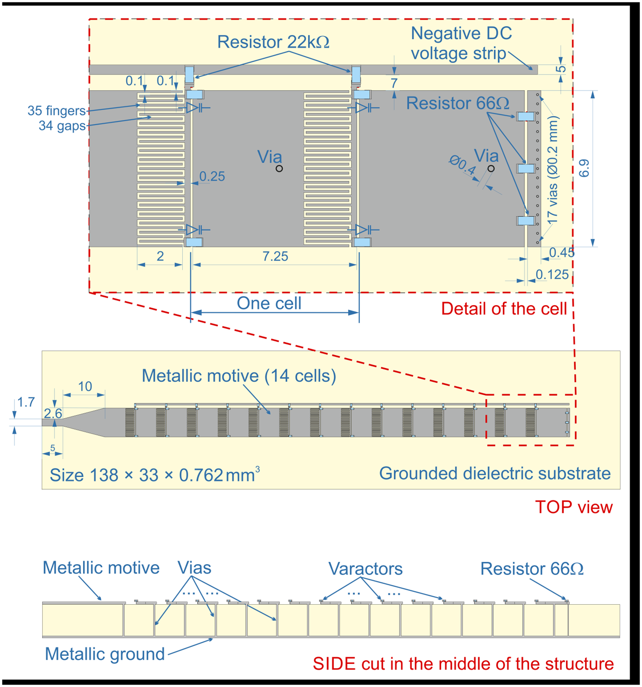
The cell has been modified to incorporate varactors that control the emitted beam by changing its capacity. Two varactors are attached to each slot between the arrays. For simple operation of the antenna, only one voltage source needs to be used, so the varactors must be connected in parallel to a DC voltage. Therefore, the conductive top patches are slotted with interdigital capacitors (IDCs) that isolate the negative ports of the varactors from the ground to which the positive ports are connected. These IDCs reduce the capacitances between the arrays and de-tune the arrays originally designed without varactors. The IDC layout was adjusted using CST MWS simulations to bring the radiation frequency back to 8 GHz. This results in IDC finger lengths equal to 2 mm and slit widths equal to 0.1 mm. There are 35 fingers in each IDC. The arrangement of the cells and array terminations is shown in detail in Fig. 2 with the basic dimensions marked.
Sketch of antenna with a detail of the cell with included varactors and resistors.

A new form of antenna termination was used. It consists of a parallel combination of three 66 Ω resistors connected through a set of 17 conductive shunts of 0.2 mm diameter to ground. These resistors model the Bloch impedance of the array determined by [Reference Sabah, Urbani and Uckun25], which is approximately 20 Ω. This termination eliminates the need for a second port that would be matched without reflection. The antenna array is composed of 14 elements to achieve sufficient traveling wave drop across its entire length. The width of the 50 Ω microstrip feed line is 1.7 mm.
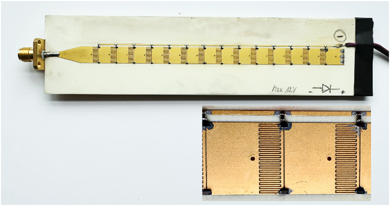
Adjacent cells are connected by two varactors that bridge the gap between them. In series with these two varactors, a resistor 22 kΩ is connected to the negative DC voltage strip (see detail in Fig. 2). In this way, all varactors are connected in parallel and only one DC voltage source can be used. The varactors used in the system are MA46H120 varactors from Macom [26]. These varactors operate with DC voltages in the range of 0 to 12 V with a corresponding capacitance change from 1 to 0.15 pF. The varactor diodes are represented in the CST MWS model by a single p-n junction capacitor only. The dependence of capacitances on DC bias voltage is given in [26].
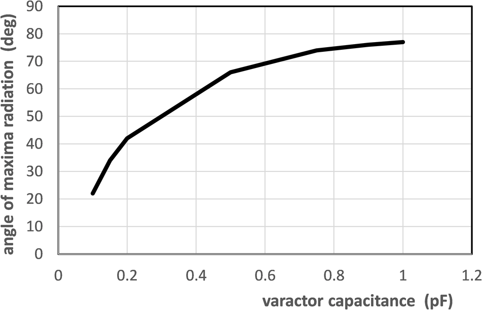
The increased capacities of the embedded varactors shift the radiation maximum of the antenna array forward. The array shall be part of a finite star structure placed on a single substrate; see Fig. 10. The individual arrays will be fed at the center of the star and must therefore radiate towards the perimeter of the structure. The dependence of the maximum radiation angle on the varactor capacitance, calculated using the CST MWS, is plotted in Fig. 3 for a frequency of 8 GHz.
Calculated dependence of the angle of maximal radiation on the varactor capacitance at 8 Ghz.

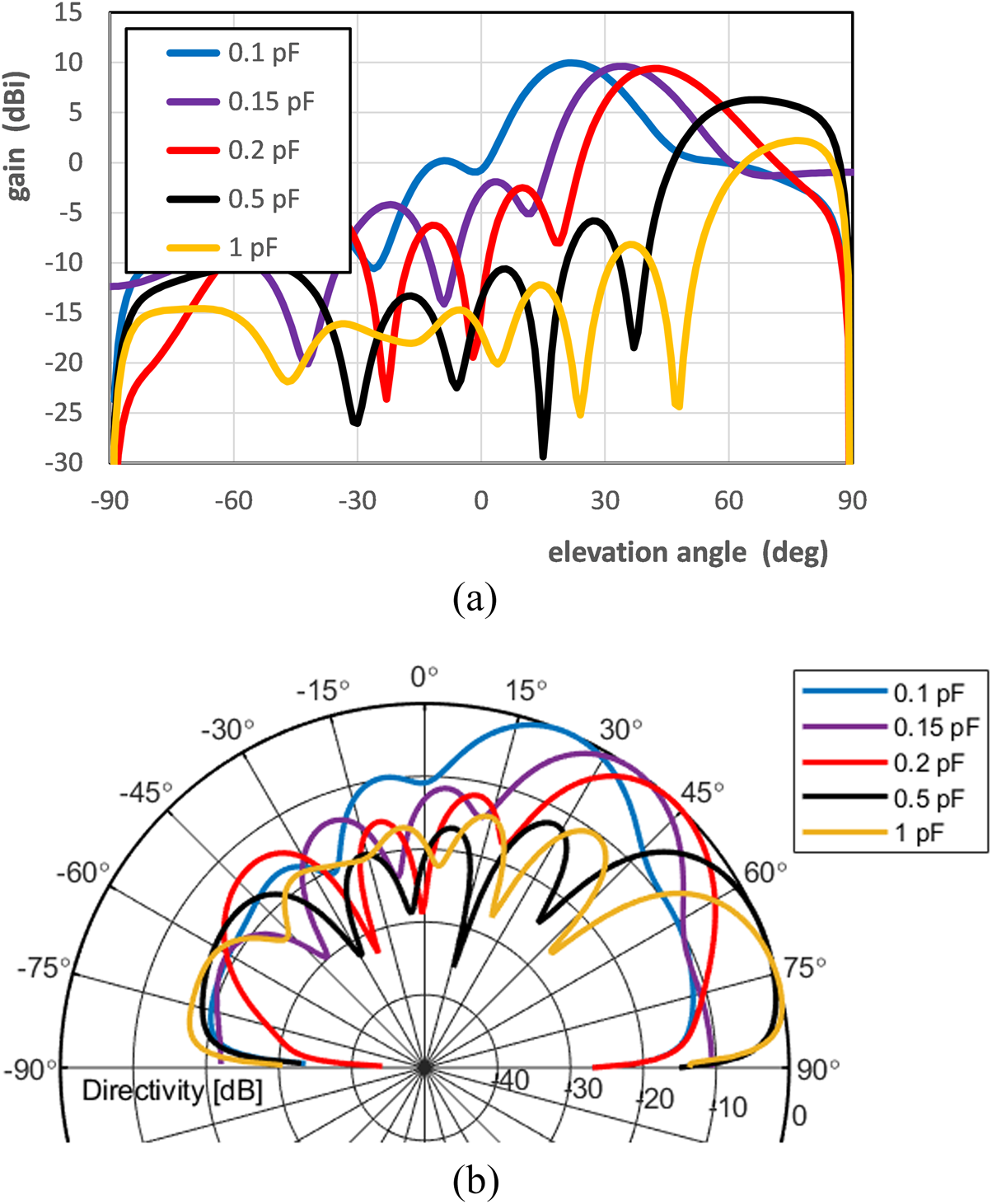
The radiation patterns calculated by CST MWS at 8 GHz are plotted in Fig. 4 for selected values of varactor capacitances. The angle θ = 0° corresponds to the broad radiation. Positive angles represent the forward direction. Figure 4 shows the approximate 55° range of elevation angles for capacitance values from 0.1 to 1 pF. It coincides with Fig. 3. The radiation is directed forward. Unfortunately, increasing the varactor capacitances reduces the gain of the antenna.
Calculated radiation patterns of the array at selected varactor capacitances at 8 Ghz. (a) Gain in rectangular coordinates, (b) normalized directivity in polar coordinates.

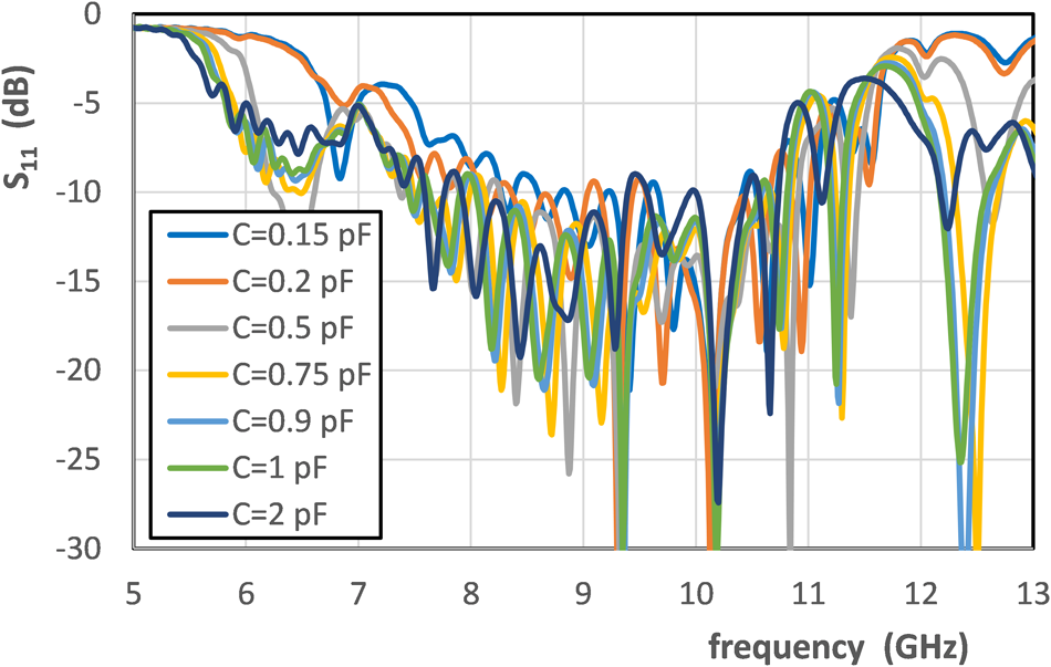
The calculated input reflectivity S 11 versus frequency for the selected varactor capacitances is shown in Fig. 5. The antenna can operate with a sufficient reflection coefficient value in the frequency band from 8 to 10.5 GHz. The exact bandwidth depends on the varactor capacity value. Increasing capacity widens this frequency band.
Calculated S 11 of the antenna array for selected varactor capacitances.

The varactor-controlled antenna array behaves similarly to a standard LWA array at the selected varactor DC bias values. The direction of maximum radiation is controlled by increasing the frequency in the forward direction.
Experiment
The antenna array designed in “Design of a varactor-controlled LWA” section was fabricated using a standard PCB process. Rogers RO4350B substrate material [27] with the parameters defined above was used. The structure is shown in Fig. 6. The varactors are connected across the slots at the conducting patch edges. The resistors 22 kΩ are connected between the patch edges and the negative DC voltage strip. The better view of this circuit is in the detail of Fig. 2. In this way, all varactors are connected in parallel and only one DC voltage source can be used.
The fabricated antenna photo with the detailed view of the cell.

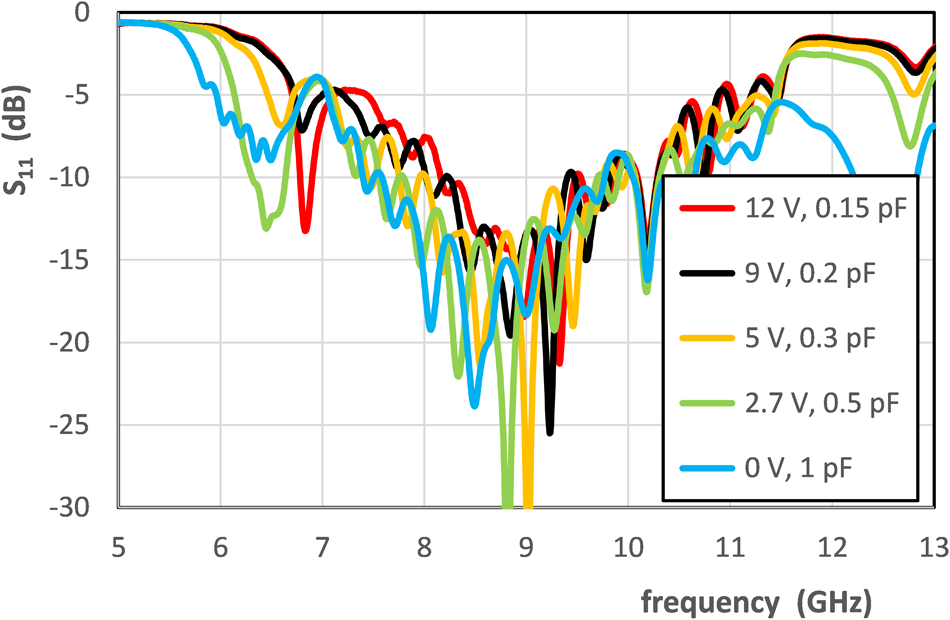
S 11 measured over a wide frequency band of 5–13 GHz is plotted in Fig. 7. The measurements were performed using a Rohde & Schwarz ZVA40 vector network analyzer (VNA) for selected voltages in the range 0–12 V. The voltages used correspond to varactor capacitances taken from [26]; see the legend of the graph. It can be seen that the measured data of S 11 agrees well with the calculated data plotted in Fig. 5.
Measured S 11 of the antenna array for selected varactor voltages.

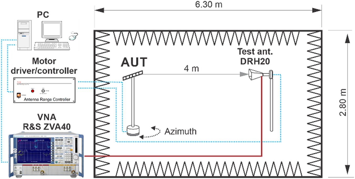
The antenna radiation patterns were measured in a full anechoic chamber using the NSI automatic scanning system for the far-field controlled by the NSI 2000 measurement software [28]. A Rohde & Schwarz ZVA40 dual-port VNA was used to measure the transmission coefficient S 21 between the antenna under test and the DRH20E test horn antenna [29]. The gain was determined by the gain transfer method using a calibrated DRH20E antenna with a known gain. The radiation pattern measurement setup is shown in Fig. 8.
Antenna radiation pattern measurement setup in the full anechoic chamber.

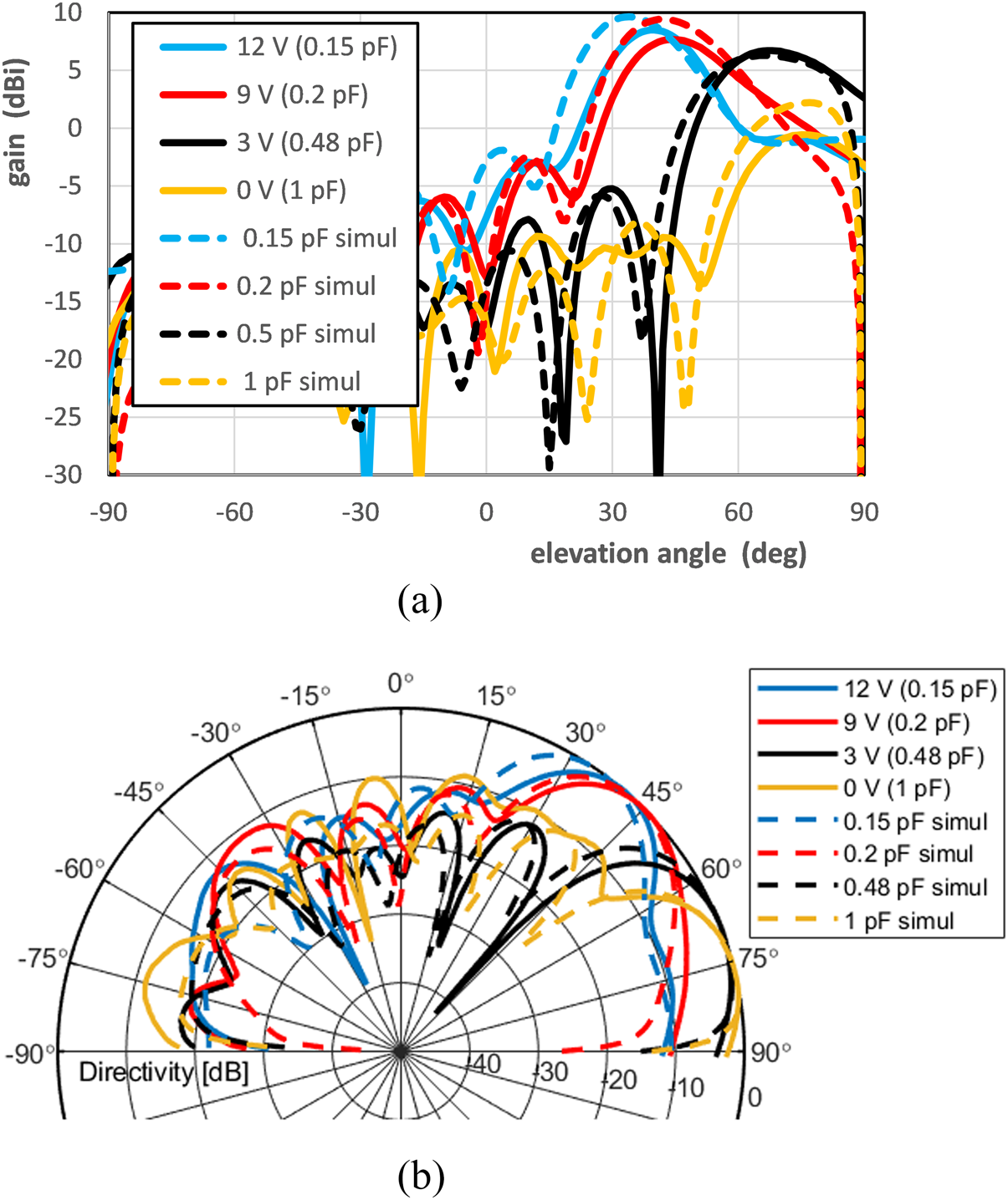
The radiation patterns measured at 8 GHz are plotted in Fig. 9 for selected DC bias voltages of varactors between 12 and 0 V. This gives the range of elevation angles 40°. Extrapolating the radiation pattern measured at 12 V, which corresponds to a varactor capacitance of 0.15 pF, to a voltage corresponding to a capacitance equal to 0.1 pF yields the range of elevation angles 50°, which corresponds to the simulated value 55°. The measured maximum gain is approximately 9 dBi. The measured side lobe level (SLL) is approximately −10 dB. Fig. 9 compares the measured and simulated data at DC voltages equal to 12 V and 0 V corresponding to 0.15 pF and 1 pF. The curves are similar except for the gain maximum.
Measured radiation patterns of the antenna array at 8 Ghz for selected varactor voltages. Dashed lines represent simulated data for corresponding capacitance values. (a) Gain in rectangular coordinates, (b) normalized directivity in polar coordinates.

The measured radiation patterns shown in Fig. 9 do not change as the frequency increases up to 8.2 GHz. Increasing the frequency further causes a narrowing of the range of elevation angles along with a decrease in the maximum gain at low values of the applied DC voltage.
Table 1 summarizes the details of selected reconfigurable antennas that have been reported in the literature. Our design offers an antenna with a wider controllable range of maximum radiation angle than previous designs [Reference Machac, Svanda and Kabourek23, Reference Machac, Svanda and Kabourek30]. The gain of 10 dBi is higher than most of the presented designs, and the SLL equal to −10 dB is similar to the antennas presented in Table 1. The used range of DC control voltage values of 0–12 V is due to the varactors MA46H120 [26] needed to provide relatively low capacitances to control effectively the radiation in elevation. The presented structure has relatively compact dimensions 3.36 × 0.88 λ0. The antenna presented in [Reference Guirado, Perez-Palomino, Carrasco, de la Rosa and Quintana11] needs very complex drivers controlling the individual liquid crystal cells. Its electrically large structure corresponds to a large gain.
The antenna with the beam steered in the whole hemisphere
The reconfigurable antenna array presented, see Figs. 2 and 6, was designed as part of an antenna with electronically controlled radiation at a constant frequency throughout the hemisphere. The arrangement of this antenna is shown in Fig. 10. The eight antennas are connected in a star geometry and are fed centrally. They are switched “ON” by PIN diodes. This switching determines the direction of radiation to selected sectors in the azimuthal plane. The radiation pattern calculated by the CST MWS at 8 GHz is plotted in Fig. 11. The horizontal left-facing array is switched “ON” and all other antennas are disconnected by PIN diodes in the “OFF” state. The capacitances of all varactors are set to 1 pF. At this value of the varactor capacitances, the antenna radiates almost in the plane of the substrate surface at an elevation angle equal to 80°, see Figs. 4 and 9. The direction of radiation in elevation is controlled, as described above, by the DC bias determining the capacitances of the varactors used, see the simulation results shown in Fig. 4 and the measured results shown in Fig. 9. The radiation patterns when the other specific antennas are “ON” are similar due to the structure symmetry.
The star antenna layout with the beam steered in the whole hemisphere.

The radiation pattern in the azimuthal plane of the antenna presented in Figure 10. Frequency is 8 Ghz, varactor capacitances are 1 pf. Only one antenna is switched “ON,” all other are in the “OFF” state.

Figure 10 schematically indicates the possible location of the bias for PIN diode switching. The central circular conducting patch serves as a common ground for all PIN diodes, while the control voltage (bias supply) of the individual PIN diodes is applied to the microstrip lines via the separation RF inductors. This is only a schematic drawing, as the exact design of the layout for switching individual PIN diodes is beyond the scope of this paper, which only aims to present the concept of this star-shaped arrangement of LWA arrays from “Design of a varactor-controlled LWA” section and “Experiment” section, respectively.
The individual LW arrays are fed by DC voltage sources separately as explained above.
Conclusion
The presented 1D LWA array was designed as a reconfigurable array composed of rectangular conducting patches placed on a dielectric substrate (mushroom cells). These patches are intersected by IDCs allowing the connection of varactors that bridge the slits between the patches. This allows the varactors to be powered from a single DC source. The controlled range of maximum radiation angles is 55° as determined by simulations performed by the CST MWS program for a range of varactor capacitances from 0.1 to 1 pF in the frequency band from 8 to 8.2 GHz. This band is the band in which the beam is steered, as described above in Figs. 4 and 9, at 8 GHz, the design frequency. The MA46H120 varactors used are recommended to operate at a DC bias voltage between 0 and 12 V, which corresponds to a capacitance range of 1 to 0.15 pF. This limits the range of measured elevation angles to 40°. The frequency band defined by S 11 < − 10 dB is 1.5 GHz and depends in detail on the DC bias voltage defining the capacitances of the varactors. The proposed antenna has a compact size and a simple structure that has been fabricated inexpensively by a printed circuit board procedure. The originality of the presented reconfigurable antenna array lies in its ability to be integrated into complex systems, as has been documented for an electronically steerable full-hemisphere beam antenna.
The presented antenna was assembled in a star configuration. Eight antennas were connected in a star structure with a central feed. The radiation patterns of these individual antennas are switched by PIN diodes to determine the specific azimuthal sector of radiation. The radiation in elevation is controlled by the DC bias of the varactors of the particular antenna array that is switched on at any given time. This reconfigurable antenna therefore represents the original antenna with the direction of the main radiation pattern electronically steerable throughout the hemisphere at a constant frequency.
Acknowledgement
This work was funded by the Czech Science Foundation through the project number GA23-07518S.
Competing interests
The authors declare none.

Jan Machac is currently a Professor with the Department of Electromagnetic Field, Faculty of Electrical Engineering, Czech Technical University in Prague, Czech Republic. He is the author or a coauthor of more than 250 publications in scientific journals and scientific international and national conferences. His main scientific interests include planar passive elements and subsystems of microwave technology, planar antennas, and microwave filters, propagation of electromagnetic waves in periodic, and artificial electromagnetic structures, chipless RFID, and power wireless transport.

Milan Svanda received the M.S. and Ph.D. degrees in radioelectronics from Czech Technical University in Prague, in 2007 and 2011, respectively. He currently a Research Scientist with CTU in Prague. He is the author or a co-author of more than 60 articles published in international journals or conference proceedings and co-author of eight patents. His main research activities are focused on antennas operating in close proximity to the human body, low-profile, and wearable RFID and sensor antennas.

Vaclav Kabourek was born in 1985. He received his M.Sc. and Ph. D. degree from the Czech Technical University in Prague in 2010 and 2017. His research interests include antenna design and measurement, RCS measurement. His contemporary research activities are also focused on EMC measurements.