Introduction
The present scenario demands highly compact and efficient devices to realize effective wireless communication with almost negligible losses. This drives researcher, academia, and industries to dive deeper into realization of highly compact structure with low-profile and low-cost devices [1, 2]. Filter-integrated antennas pronounced as filtennas are one among such devices that come with multi-functional characteristics with miniaturized in size, as it delivers filtering and radiation properties simultaneously with minimal delay and losses. Owing to this, filtennas are highly demanding for integrated wireless communication and RF front-end systems [Reference Rao and Ram3].
In early days, microstrip filtennas were researched and designed by integrating antennas and filters together. In reported filtennas, filtering characteristics such as selectivity and out-of-band rejection are in good level, whereas low-level gain and high radiation losses lag the performance of filtenna [Reference Tang, Shi and Ziolkowski4–Reference Ranjan and Kumar7]. Substrate integrated waveguide (SIW) technology overcomes the issues that were occurring in the microstrip topology. It has multiple advantages over microstrip, i.e. highly compact, low radiation and conducting loss, low fabrication cost, and high-power handling capacity to produce high gain. However, due to high-density integration, some leakage loss can be considered [Reference Sun, Ma, Feng, Shi and Xu8]. In [Reference Liang, Wang and Dong9], a cavity-backed SIW antenna is reported with a gain value of 7 dBi across the pass band, which is quite good as compared to microstrip antennas. Similarly, SIW antenna based on these topologies with single- and dual-pass band are reported in [Reference Ho, Pistono, Corrao and Ferrari10] and [Reference Shen, Geng, Yang, Yang and Chen11].
Various SIW topology-based filtennas have been reported till date for different applications [Reference Hu, Tang, Li and Ziolkowski12–Reference Hu, Guo, Pan, Yan, Tang and Wang23]. In [Reference Hu, Tang, Li and Ziolkowski12], a multilayer-structured SIW filtenna is presented with 6.3% fractional bandwidth (FBW) and 6 dBi gain. Similarly, a filtenna with two radiation nulls (RNs) and 5.8 dBi gain with 2.5% FBW, designed on a single layer, is presented in [Reference Wang, Wang, Liu, Chen and Han13]. A planar wideband filtenna with 9% FBW and more than 7dBi gain is discussed in [Reference Liu, Zhu, Wang and Wu14]. A synthesis approach-based filtenna with a parasitic patch as a radiator is presented in [Reference Hu, Tang, Li, Wang and Li15], in which two RNs and more than 12 dB out-of-band rejection with 5% FBW and 6 dBi gain are achieved. A single cavity backed and resonator topology-based filtenna with wideband response of 11.8% FBW is discussed in [Reference Yin, Bai, Deng, Ren, Sun, Zhang and Guo16]. The presented filtenna have two RNs generated by resonators with 5 dBi pass band gain along with more than 8 dB out-of-band suppression level. A compact SIW resonator-based hybrid filtenna with 7 dBi gain two RNs and 5% FBW is presented in [Reference Li and Deng17]. In [Reference Zhao, Lin, Sun and Zhang18], a dual-band pass filtenna with multi-layered structure and three RNs is discussed, and filtenna with three passband response and six RNs is reported in [Reference Zheng, Li, Tan and Chen19]. However, both the filtenna suffer with narrow band response and 5 dBi maximum gain in pass band. A slot-based topology followed dual-band SIW filtenna with a very wide stop band and three RNs is reported in [Reference Zhou, Zhang, Tam, Lin and Zhang20]. However, it has 5.5% FBW and 6.3 dBi pass band gain. A planar structured and differential feed SIW filtenna with 9% FBW, 7.7 dBi gain with more than 13 dB out-of-band rejection level is discussed in [Reference Hu, Yuan, Li, Tang, Chen and Yan21]. In [Reference Li, Zhang, Liu, Liu, Li, Yang, Xu, Wang, Yang and Tang22], a triplex filtenna designed with SIW and slot topology is presented with 7.1 dBi pass band gain, 11 dB out-of-band rejection, and FBW of nearly 4%. A planar SIW filtenna designed with a parasitic patch and defected ground structure is discussed in [Reference Hu, Guo, Pan, Yan, Tang and Wang23]. This filtenna have FBW of 9.2% and 5.75 dBi pass band gain with two RNs and 11 dB out-of-band rejection level. Further application of SIW filtenna is also exposed to array configuration [Reference Yan, Huang, Tang and Chen24] and [Reference Huang, Yan, Tang, Yu and Chen25]. Although gain has increased to more than 10 dBi but they suffer a lesser bandwidth.
In this paper, an LPF-integrated SIW filtenna with multiple RNs, good selectivity along with wider pass band is presented. The detailed design mechanism of SIW filtenna has been discussed in Section “Mechanism of proposed highly selective SIW filtenna,” in which equivalent circuit model (ECM) of proposed filtenna is also discussed. The performance analysis of the proposed SIW filtenna is presented in Section “Results and discussion,” followed by concluding remarks in Section “Conclusion.”
Mechanism of proposed highly selective SIW filtenna
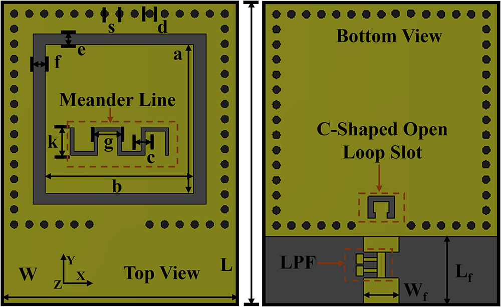
The structural layout of the proposed SIW filtenna fed with 50-ohm microstrip line is shown in Fig. 1. The filtenna is designed on the Rogers RT 5870 substrate having 1.57 mm thickness with permittivity of 2.33. The cavity of filtenna followed the design and spacing rules for via holes is s/d ≥ 2. Calculation of optimized resonant frequency can be obtained from Equation (1) [Reference Hu, Yuan, Li, Tang, Chen and Yan21].
Design configuration of proposed SIW filtenna. L = 40, W = 31, LF = 9, WF = 4.7, a = b = 19.7, c = 0.5, d = 1, s = 2, e = 1.45, f = 1.65, g = 3.6, k = 3.6, m1 = 3.5, m2 = 0.7, m3 = 1.5, m4 = 2.9, LF 1 = 0.75, LF 2 = 1, LF 3 = 1, LF 4 = 1.4, LF 5 = 0.5, LF 6 = 1.8, GP = 0.2, W1 = 1.1 mm.

The operational mechanism of the proposed antenna can be understood by the mode analysis. The modes can be calculated by Eigen mode solver tool of the CST software. It is observed that two different modes TE310 and TE230 existed within the cavity at 11.5 and 13 GHz, respectively, as shown in Fig. 2. As two modes are obtained in the operating frequency band (11–13.1 GHz), the two resonant frequencies are also obtained within the operating frequency in the S11 (dB) of simulation of the SIW antenna configurations, as shown in Fig. 3(a). Initially, the closed-loop slot is removed from the top of the cavity which produces the response of antenna. The removal of slot produces the first RN at 7.7 GHz with a gain value of −9.8 dBi, as shown in Fig. 3. In the next step, a LPF is integrated with the feedline of antenna. This LPF generates another RN at 13.4 GHz, which realizes the filtenna property. To sharpen the selectivity at lower side, a meander-line structure designed at half wavelength at 10 GHz is removed from the radiator. This removal step improves the reflection coefficient response and generates another RN at 10 GHz. Similarly, a C-shaped open loop slot (CSOLS) designed at half wavelength at 14.1 GHz is removed from the bottom side of the cavity, which is placed near the feedline of filtenna. This step shows a significant impact on the response of reflection coefficient as well as the gain curve. The removal of this slot creates another RN at 14.1 GHz with a gain value of −20 dBi and improves the levels of other RNs, which improves the overall selectivity of filtenna.
 \begin{equation}{f_{mn0}} = \frac{c}{{2\sqrt {\mu \in } }}\sqrt {{{\left( {\frac{m}{W}} \right)}^2} + {{\left( {\frac{n}{W}} \right)}^2}} \end{equation}
Electric field distributions (a) at 11.5 GHz (TE310) and (b) 13 GHz (TE230).

(a) S11 (dB) of different configurations. (b) Gain of different configurations.

Furthermore, as in the proposed SIW filtenna four RNs are obtained by incorporating the various slots and an LPF, as shown in Fig. 3(b). The first RN at 7.7 GHz is obtained by the removal of loop quadrilateral slot. The dimension of this loop is determined by calculating the value of wavelength ( ${\lambda _0}$) at 7.7 GHz. The formula, used for calculation, is mentioned in Equation (2), where c is the speed of light and
 ${f_0}$is the corresponding frequency.
 \begin{equation}{\lambda _0} = \frac{c}{{{f_0}}}\end{equation}
The calculated value for a loop is obtained as approximately 39 mm. After optimization with proper impedance matching, the value of this loop is increased to 78.8 mm, which is almost twice of the calculated fundamental wavelength. Similarly, for the third RN, the calculation of meander-line slot at 10 GHz is carried out at the fundamental wavelength and the value is obtained as 30 mm calculated by using Equation (1). Finally, for the fourth RN, the length of CSOLS at 14.1 GHz is calculated at the half of the fundamental wavelength ( $\frac{{{\lambda _0}}}{2}$). The obtained value for this slot is 11 mm. Overall, in the final design of the proposed SIW filtenna, the length of the loop quadrilateral slot is chosen at
 $\left( {2{\lambda _0}} \right)$ twice of the fundamental wavelength,
 ${\lambda _0}$ for the meander-line slot and
 $\frac{{{\lambda _0}}}{2}$ for the CSOLS, which generates three different RNs at the respective frequency.
The length of meander line directly impacts on the position of the third RN. As depicted in Fig. 4(a), a decrease in the length shifts position of the RN to upward and reduces the maximum gain value and vice versa. Hence, the optimized overall length of meander line is obtained as 32 mm. Similarly, the length of CSOLS is affecting the position of the fourth RN. As the length decreases, the RNs starts shifting upwards with reducing the maximum gain value and vice versa. An optimized length value is noted as m1 = 3.5 mm, as shown in Fig. 4(b).
(A) Effect of meander-line length (MLL). (b) Effect of CSOLS length.

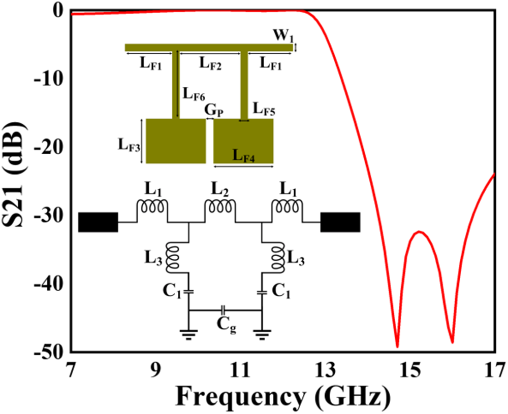
Further working mechanism of filtenna (filter and antenna) is investigated through the ECM analysis. ECM of the LPF along with its transmission-line structure is depicted in Fig. 5. LPF can be modelled with inductor and capacitor according to the inductive line and capacitive stub. The gap between two capacitive stub is represented by gap capacitor, which creates another transmission zero, as shown in the same figure [Reference Kumar and Parihar26]. Calculation of lumped element values (inductor  ${L_i}\,\left( {i\, = \,1,\,2\,,\,3} \right)$ and capacitor
 ${C_1}$) is followed by Equations (3) and (4), where,
 ${{\text{Z}}_{Hj}}\left( {j{\text{ = L}}{{\text{F}}_{\text{1}}}{\text{,}}\,{\text{L}}{{\text{F}}_{\text{2}}}{\text{,}}\,{\text{L}}{{\text{F}}_{\text{6}}}} \right)$ and
 ${Z_{LF3{\text{ }}}}$ are the impedance of inductive and capacitive line, respectively. Phase constant and length of respective lines are denoted by
 ${\beta _{Hj{\text{ }}}}$ and
 ${L_{j{\text{ }}}}$and
 ${L_{F3{\text{ }}}}$, respectively, while
 ${f_c}$ is the cutoff frequency, obtained as 13.1 GHz. The optimized value of LC model of LPF is as follows:
 ${L_1} = {\text{ }}0.527nH$,
 ${L_{2{\text{ }}}} = {\text{ }}0.906nH$,
 ${L_{3{\text{ }}}} = 0.789nH$,
 ${C_1} = {\text{ }}0.18pF$, and
 ${C_g}\, = \,\,0.0006pF$
 \begin{equation}{L_i} = \frac{{\left( {{Z_{Hj{\text{ }}}} \times {L_{j{\text{ }}}} \times {\beta _{Hj{\text{ }}}}} \right)}}{{2\pi {f_c}}}{\text{ }}\end{equation}
 \begin{equation}{C_1} = \frac{{\left( {{L_{F3{\text{ }}}} \times {\beta _{LF3{\text{ }}}}} \right)}}{{{Z_{LF3{\text{ }}}} \times {\text{ }}2\pi {f_c}}}{\text{ }}\end{equation}
Layout and ECM of LPF with S21(dB) curve.

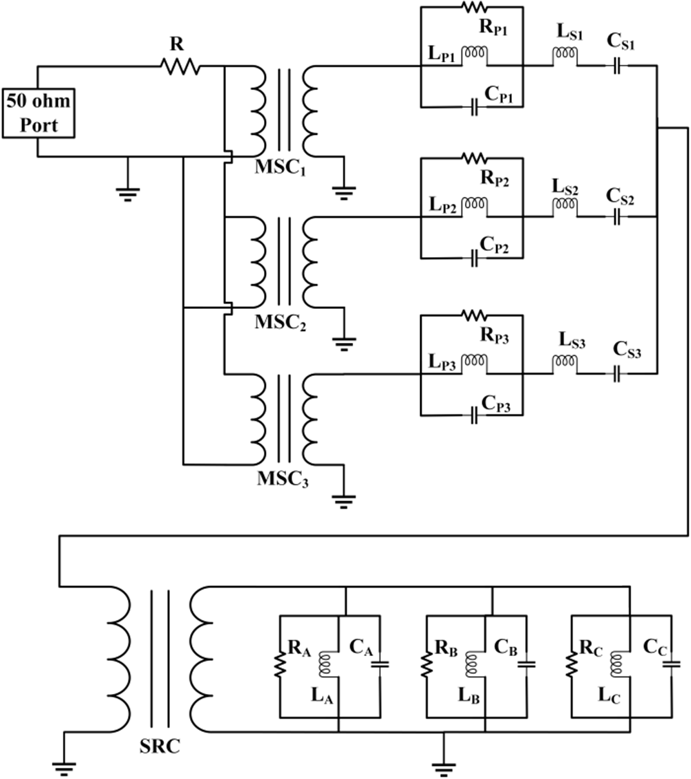
In the next stage, ECM of SIW antenna is designed and optimized with the matching of CST software simulated reflection coefficient [27]. As in electromagnetic model (EMM), three resonant frequencies are observed at 11.5, 12.4, and 13 GHz. Hence, three ideal transformers (MSC1,2,3) are taken for microstrip feedline to SIW cavity coupling, with three parallel RLC circuit combinations (R/L/C (P1, P2, P3)). Furthermore, three series LC circuits (L/C (S1, S2, S3) are connected with the each one of the parallel RLC circuit, which accounts for the loading effect between the different resonating frequency cavity. To manage the feedline inherent ohmic losses, a small resistance (R) is included in the circuit. In next, the cavity is further coupled with the radiator slot by another ideal transformer (SRC). Furthermore, the ECM of the radiator is modelled as parallel RLC circuit (RA, LA, CA). Lastly, two more parallel RLC circuit (RB/C, LB/C, CB/C) is added to accommodate the effect of meander-line slot and CSOLS responses [Reference Mukherjee and Biswas28]. The modelled ECM of SIW antenna is depicted in Fig. 6, and the governing equation can be given by Equations (5–8), and  ${S_{11}}$ is the reflection coefficient of the SIW antenna.
Normalized far-field radiation pattern. (a) E-plane at 11.5 GHz. (b) H-plane at 11.5 GHz. (c) E-plane at 13 GHz. (d) H-plane at 13 GHz.

 \begin{equation}{Z_{in}} = \frac{{1 + {S_{11}}}}{{1 - {S_{11}}}}{\text{ }}\end{equation}
 \begin{equation}\frac{1}{Z} = {\text{ }}\frac{1}{R} + {\text{ }}\frac{1}{{j{\omega _L}L}} + j{\omega _L}C = A + jB{\text{ }}\end{equation}
 $\left( {\text{where Z}}\right. = {{\text{Z}}_{{\text{in}}}}{\text{*}}50{\text{ and }}{{{\omega }}_{\text{L}}} = 2{{\pi }}{{\text{f}}_{0{\text{L }}}}\left( {{\text{f}}_{0{\text{L }}}} = {\text{corresponding }} \right.$
 $\left.\text{resonant frequency} \right)$
ECM of SIW antenna.

 \begin{equation}{f_{0U{\text{ }}}} = {\text{ }}\frac{1}{{2\pi \sqrt {LC} }}{\text{ }}\end{equation}
 \begin{equation}{Q_{U{\text{ }}}} \approx {\text{ }}\frac{{{f_{0U{\text{ }}}}}}{{{f_c}}} = {\text{ }}\frac{R}{{j{\omega _U}L}}\end{equation}
 $\left( {\text{where }}{{{\omega }}_{\text{U}}} \right.= 2{{\pi }}{{\text{f}}_{0{\text{U }}}} \left({{\text{f}}_{0{\text{U }}}} = {\text{unloaded resonant frequency}} \right.$
 $\left.\text{obtained by eigen mode solver and }{{\text{f}}_{\text{c}}}{\text{ is the center frequency}} \right)$
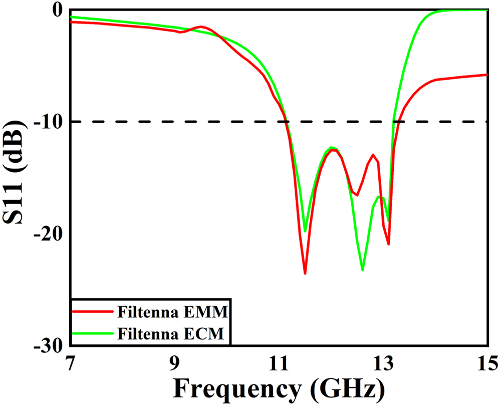
By using Equations (5–8), for the resonant frequencies at 11.5, 12.4, and 13 GHz, the values of RLC are calculated and optimized to match with the EMM (CST simulation) results. Initially, the coupling coefficient (turn ratio) of the ideal transformer kept at 1 but further optimized to the respective values of MSC1,2,3 = 0.22 and SRC = 3. The value of resistance R (chosen to accommodate with inherent ohmic losses) is chosen as 1 and further it is optimized to 0.5 Ω. The remaining values are calculated by using Equations (2–5). In the final stage, ECM of filter and ECM of antenna is integrated together, which generates the filtenna response matched with the EMM of filtenna, as shown in Fig. 7. The optimized value of ECM model of SIW antenna is as follows: R = 0.5 Ω, MSC1 = MSC2 = MSC3 = 0.22, RP1 = 3.1 Ω, RP2 = 3.3 Ω, RP3 = 3.7 Ω, RA = 0.8 Ω, RB = 0.6 Ω, RC = 0.7 Ω, LP1 = 1.54nH, LP2 = 1.78nH, LP3 = 1.34nH, LS1 = 0.43nH, LS2 = 0.4nH, LS3 = 0.43nH, LA = 0.48nH, LB = 0.38nH, LC = 0.58nH, CP1 = 0.18pF, CP2 = 1.26pF, CP3 = 1.41pF, CS1 = 0.36pF, CS2 = 0.51pF, CS3 = 0.31pF, CA = 0.52pF, CB = 0.42pF, CC = 0.62pF, SRC = 3.
Reflection coefficient (S11 (dB)) of ECM and EMM model of filtenna.

Results and discussion
The proposed SIW filtenna has been verified by its fabrication and measurement. The proposed SIW filtenna is fabricated by LPKF S103 Machine, whereas testing has performed with the help of Agilent E5071C VNA. The snapshot of fabricated structure of proposed SIW filtenna is shown in Fig. 8. The measured FBW of antenna is of 17% (11–13.1 GHz) with closely matched to the simulated S11(dB) curve of filtenna. The peak gain of filtenna is of 8.56 dBi is measured with four RNs in the stop band, as shown in Fig. 9. The simulated efficiency of filtenna is above 80% in the pass band and below 25% in the stop band. We observed that the out-of-pass band rejection level is 15 dB at lower edge and 22 dB at upper edge. The selectivity of the proposed filtenna can be measured by lower edge FL and upper edge FU [Reference Zhou, Zhang, Tam, Lin and Zhang20]. The obtained value of FL and FU are 0.65 and 0.05, respectively, which show that the proposed SIW filtenna is highly selective in nature with wider pass band response.
Snapshot of fabricated SIW filtenna.

Simulated and measured S11(dB) and gain with simulated efficiency.

Surface current distribution of filtenna is depicted in Fig. 10. It is determined from the figure that current is distributed throughout the radiator in frequency of pass band, while current is completely concentrated around the LPF at out-of-pass band frequency. Normalized far-field radiation patterns are stable with low cross-polarization value in both the planes (E-Plane and H-Plane) at 11.5 and 13 GHz, respectively, as shown in Fig. 11. The proposed SIW filtenna is compared with the earlier reported state-of-the-art filtennas (Table 1), which shows that the presented SIW filtenna is a good candidate for the short-range radar system, satellite communication (uplink and downlink), IoT-based indoor and outdoor communications, surveillance applications, and modern RF front-end systems.
Surface current distributions at (a) 11.5 GHz and (b) 14 GHz.

Comparison of proposed work with current reported SIW filtennas

Abbreviations: Ref. = Reference; Size = λ0 × λ0 (where λ0 is the free-space wavelength at the center frequency for the antenna), OFR = Operating Frequency Range in GHz; FBW = Fractional bandwidth in %; RN = No. of Radiation Null; RL = Rejection Level (lower edge/upper edge); FL = Lower edge selectivity; FU = Upper edge selectivity; Gain = dBi; PW = Proposed work.
Conclusion
A highly selective SIW filtenna integrated with an LPF with low-profile and compact structure is discussed in this section. The removal of meander-line slot and C-shaped slot improves the selectivity and impedance bandwidth significantly. The analysis of ECM explains the working mechanism of filtenna, which closely matched with the result of EMM. The proposed filtenna has FBW of 17% and a peak gain of 8.56 dBi, with four RNs. The lower edge selectivity is 0.65 with 15 dB out-of-band rejection, while upper edge selectivity is 0.05 with 22 dB out-of-band rejection level. With these promising characteristics, the proposed SIW filtenna can be the best suitable candidate for the short-range radar system, satellite communication (uplink and downlink), IoT-based indoor and outdoor communications, surveillance applications, modern RF front-end systems, and modern wireless communication applications.
Competing interests
The authors report no conflict of interest.

Abhishek Patel received his B.E. degree in Electronics Engineering from MITS Gwalior, India, in 2018 and M.Tech. degree in Microwave and Communication Engineering from PDPM-IIITDM Jabalpur, India, in 2020. He is currently pursuing his Ph.D. degree in Microwave and Communication Engineering from PDPM-IIITDM Jabalpur, India. His current research interests include ultra-wideband antenna and filtenna for RF front-end systems.

Trivesh Kumar received his PhD in Electrical Engineering from Indian Institute of Technology Kanpur, India. He is presently an assistant professor in the Department of Electronics and Communication Engineering, Indian Institute of Information Technology, Design and Manufacturing, Jabalpur, India. The main areas of his research feature circularly polarized antennas and analysis, microwave-measurements, RFID, substrate-integrated waveguide structures, and many more.

Manoj Singh Parihar received his BE and MTech degrees from RGPV Bhopal, Bhopal, India, in 2001 and 2004, respectively, and a PhD degree from IIT Delhi, New Delhi, India, in 2012. From 2010 to 2013, he was senior project scientist with the Center for Applied Research in Electronics (CARE), IIT Delhi. In 2007, he received an Institute of Electronics and Telecommunication Engineers (IETE) Research Fellowship for continuing his research work in reconfigurable antennas at IIT Delhi, and simultaneously, he was selected for the invitation programme sponsored by the National Institute of International Education (NIIED) of the Ministry of Education and Human Resources of Republic of Korea to visit Korean Universities and Industries. He is currently assistant professor with the Indian Institute of Information Technology, Design and Manufacturing (IIITDM) Jabalpur, Jabalpur, India. His current research interests include reconfigurable antennas, microwave integrated circuits, microwave and millimeter-wave device characterization, and RF MEMS.