
I. INTRODUCTION
Over the past several decades, zinc oxide (ZnO) has been the focus of semiconductor research as a high band gap direct material, with the goal of improving its properties for optoelectronic applications and transparent electronics. ZnO nanostructures, such as nanowires and nanobelts, have also been intensively studied for their use as chemical sensors, Reference Ramgir, Yang and Zacharias1 UV photodetectors, Reference Guo, Zhang, Zhao, Li, Zhang, Jiang and Shen2,Reference Soci, Zhang, Xiang, Dayeh, Aplin, Park, Bao, Lo and Wang3 or as piezoelectric devices. Reference Wang and Song4 Possible applications based on ZnO bulk or layer systems cover transparent thin film transistors (TTFT), Reference Hoffman, Norris and Wager5,Reference Grundmann, Frenzel, Lajn, Lorenz, Schein and von Wenckstern6 surface acoustic wave (SAW) filters, Reference Du, Fu, Tan, Luo, Flewitt, Maeng, Kim, Choi, Lee, Park, Park and Milne7 or buffer layers and sacrificial substrates for the growth of gallium nitride (GaN). Reference Ougazzaden, Rogers, Hosseini Teherani, Moudakir, Gautier, Aggerstam, Ould Saad, Martin, Djebbour, Durand, Garry, Lusson, McGrouther and Chapman8–Reference Detchprohm, Hiramatsu, Amano and Akasaki10 To meet the special demands for the large number of different applications, various possibilities for synthesizing ZnO have been investigated, and the growth of single crystalline material Reference Maeda, Sato, Niikura and Fukuda11 as well as nanostructures in a variety of morphologies has been reported. Reference Wang12 In addition to sophisticated and expensive growth methods like molecular beam epitaxy (MBE) Reference Wang, Iwaki, Murakami, Du, Ishitani and Yoshikawa13 or metalorganic vapor phase epitaxy (MOVPE), Reference Ogata, Kawanishi, Sakurai, Kim, Maejima, Fujita and Fujita14,Reference Oleynik, Adam, Krtschil, Bläsing, Dadgar, Bertram, Forster, Diez, Greiling, Seip, Christen and Krost15 which allow for outstanding crystalline quality and control, a large number of publications are focused on the less expensive wet-chemical growth of ZnO. Reference Ouerfelli, Regragui, Morsli, Djeteli, Jondo, Amory, Tchangbedji, Napo and Bernède16,Reference Ortega-López, Avila-García, Albor-Aguilera and Sánchez Resendiz17 The technical realization of these low-temperature methods is considered to be straightforward, and a high flexibility in the choice of the substrate is possible. However, the crystalline quality grown by these methods cannot reach the level obtained by high-temperature growth methods.
The ZnO growth method presented here is based on a chemical vapor deposition (CVD) process, which fulfills both requirements of good controllability of the growth conditions as well as technical simplicity, which are crucial for industrial up-scaling. By using methane (CH4) as a precursor to reduce the ZnO source material, it is possible to control the source material consumption - and in this way the final II–IV ratio - very precisely. With this method, high growth rates and high crystal quality have been realized. By appropriately adjusting the growth conditions, it is possible to switch between the growth of layers and of nanowires, even while using the same CVD process and setup. In our experiments, ZnO nanowires have been grown catalyst-free on c-plane as well as on a-plane sapphire, and their excellent optical properties are established using low-temperature photoluminescence (PL) spectroscopy.
II. EXPERIMENTAL
A. CH4 as a precursor for the growth of ZnO
The growth of ZnO layers and nanowires was established in a three-zone tube furnace (Carbolite HZS 12/600, Carbolite Gero GmbH & Co. KG, Neuhausen, Germany) with a horizontal quartz glass liner tube. On the upstream-side, three gas inlets are located for argon (99.998%), oxygen (99.995%), and CH4 (99.5%). Three computer controlled mass flow controllers (MFCs) are used for the precise intake of the different gases. A closed-loop regulated vacuum pump is connected to the downstream side, stabilizing the tube pressure at 930 mbar. As source material, 0.5 g of a commercially available ZnO powder (99.9%, Grillo Zinkweiss Pharma 8, Gillo Zinkoxid GmbH, Goslar, Germany) is placed in a quartz glass boat on the upstream side of the furnace and heated to 910 °C under argon atmosphere. To obtain elemental zinc vapor, CH4 is added as a reductant as soon as the final process temperature is reached. The reduction of the source material follows the simple chemical equation Reference Steinfeld, Brack, Meier, Weidenkaff and Wuillemin18,Reference Ale Ebrahim and Jamshidi19 :
 $${\rm{ZnO}} + {\rm{C}}{{\rm{H}}_4} \to {\rm{Zn}} + 2{{\rm{H}}_2} + {\rm{CO}}\quad .$$
The elemental Zn vapor generated is transported by the argon stream (50 mL/min) to the substrate, which is located in a lower temperature region downstream from the source material boat. Together with additional oxygen, which is added to the main Ar stream, the Zn vapor oxidizes again, and crystalline ZnO is deposited on the substrate. The high argon stream dilutes the inflammable gas mixture to prevent the direct burning of CH4 in the presence of O2. Reference Cheng and Luo20–Reference Razus, Molnarne and Fuß22 Moreover, the temperature is too low to ignite the gas mixtures used in our growth experiments. Reference Zabetakis23 A part of the CH4 might be lost by the oxidation, but the majority leads to direct reduction of the ZnO powder to elemental Zn vapor. A part of the diluted O2 must also be left over to re-oxidize this Zn to ZnO on the surface of the substrate.
With this configuration, either ZnO layers or nanowires can be grown on different substrates by adjusting the gas flows and substrate temperature. An important control parameter is the flux of oxygen added on the upstream side of the system. We do not use an additional O2 insertion tube, showerhead etc., and therefore we expect an up-scaling to larger growth setups to be straightforward. Even in our small system with an inner tube diameter of only 40 mm, a homogeneous growth over several cm2 has been achieved, implying that the zone of homogeneous growth conditions (i.e., a constant II–VI ratio) is relatively large as compared to systems using a small diameter lance for oxygen insertion at the location of the substrate. On the other hand, the addition of oxygen to the main gas stream leads to a partial re-oxidation of the elemental Zn vapor generated before the latter reaches the substrate. In Sec. III we discuss the interrelation of source material consumption, CH4 and O2 flux in more detail.
B. ZnO seed layer growth
For the growth of ZnO, c- and a-plane sapphire are used as substrate materials. To avoid the use of a metallic catalyst which might be partially incorporated in the resulting layers or nanostructures, a ZnO seed-layer is deposited in a prior growth step using the same CVD setup. For this purpose, 0.5 g of zinc acetate dihydrate (Zn(CH3COO)2·H2O, 99.5%, Alfa Aesar GmbH & Co. KG, Karlsruhe, Germany) is sublimated by heating it to 190 °C. Using an argon gas stream (76.5 mL/min) mixed with 4.6 mL/min of oxygen, the sublimated acetate is transported to the substrate, which is placed in a region with a temperature of 500 °C. The whole process takes only 2 min after the temperatures are reached, and is performed at 550 mbar. In this step, a thin layer (with a few nm thickness) of polycrystalline ZnO seeds is deposited. These seed crystals serve in the subsequent main process as nucleation sites for the growth of ZnO layers and nanowires. Further details about the seed layer formation can be found in Ref. Reference Reiser, Raeesi, Prinz, Schirra, Feneberg, Röder, Sauer and Thonke24.
C. Conventional carbo-thermal growth of ZnO nanowires
For comparison of the quality, we have also grown ZnO nanowires by the carbo-thermal technique. In this process, the ZnO source material (99.99%, Alfa Aesar) is mixed with graphite powder (99.9999%, Alfa Aesar). For the growth, 140 mg of the mixture is heated up to 1050 °C under pure argon atmosphere at 900 mbar. Instead of CH4, carbon now reduces the ZnO powder, leading to elemental Zn in the vapor phase, which is transported to the substrate by the main argon stream (160 mL/min). Directly above the substrate (at 1060 °C), oxygen is introduced to the system using a thin quartz glass lance, locally oxidizing the Zn vapor and forming ZnO on the substrate. With this procedure nanowires were grown either on sapphire with the ZnO seed layer described above, or on silicon (111) substrates using a 3 nm thin gold layer serving as catalyst. A detailed description of the carbo-thermal growth processes can be found in Refs. Reference Subannajui, Ramgir, Grimm, Michiels, Yang, Müller and Zacharias25 and Reference Li, Feneberg, Reiser, Schirra, Enchelmaier, Ladenburger, Langlois, Sauer, Thonke, Cai and Rauscher26.
D. Characterization
The morphology of the grown samples was characterized using a SEM with a field-emitter cathode (Zeiss Leo DSM982, Carl Zeiss Microscopy GmbH, Oberkochen, Germany). The optical properties were investigated by low-temperature (T ≈ 5 K) PL spectroscopy using a cw HeCd-laser (Kimmon Koha Co. Ltd., Tokyo, Japan) operated at 325 nm wave length for excitation. The light emitted from the sample was recorded by a liquid nitrogen cooled CCD camera attached to a grating monochromator with a 1 m focal length.
III. RESULTS AND DISCUSSION
A. Reduction of the source material by CH4
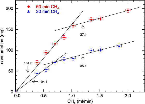
In our growth studies, the most crucial parameter for the successful growth of ZnO nanowires using CVD-based methods was the consumption of the source material, which controls the partial pressure of Zn during the growth. In most vapor-transport based methods, ZnO powder mixed with carbon is commonly used as the source material, having the disadvantage that the amount of Zn in the vapor phase cannot be controlled directly. In the method presented here, we substitute the graphite powder by a CH4 gas, enabling a precise control over the source material consumption and hence the Zn concentration in the vapor phase. To characterize the consumption in our growth process, we reduced 0.5 g of the ZnO source material using different CH4 flows without adding additional oxygen to the system. Figure 1 shows the measured consumption after 30 min and after 60 min of elapsed time. Without CH4 added to the argon stream, no reduction occurred, and thus no source material was consumed. By increasing the CH4 flow, a linear increase of source material consumption was found, leading–as expected–to a linear interdependence (i.e., a line through the origin). A clear change in the slope was found for both series when the CH4 flow was further increased. We attribute this lower consumption rate for higher CH4 flow to the limited amount of source material available in our system. We found that the size of the source boat and especially the area covered by the ZnO powder is a crucial factor for the reduction rate. If the same amount of source material was spread over a larger area, a higher consumption was measured, due to the larger surface available for the chemical reaction. Increasing the flow even further still led to higher consumption, but at a significantly reduced rate. In this region of higher flow, we observe a linear dependence, showing approximately the same slope for both reduction time intervals (see Fig. 1).
Dependency of the source material consumption on the CH4 flow. 0.5 g of the ZnO source material have been reduced at 910 °C for 60 min (red dots) or 30 min (blue triangles) respectively, using different CH4 fluxes. The numbers at the arrows are the slopes of the respective linear regressions.
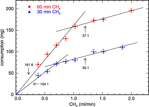
Comparing the absolute values obtained for both series, it appears that the consumption was not exactly doubled when doubling the reduction time. This is clearly seen for the small CH4 fluxes, where a difference is obvious. Nevertheless, the values have the expected magnitude when taking the indicated errors into account. The linear dependency of the reduced material on the CH4 flow found in this consumption series shows a very good control of the reduction, and hence of the amount of Zn in the vapor phase. This is especially true in the regime of higher CH4 flows, where a smaller slope of the linear regression was observed, and the amount of reduced source material can be adjusted very precisely.
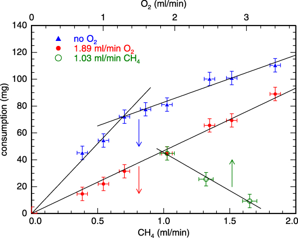
For the realization of ZnO growth, additional O2 has to be added to the gas flow. For simplicity, the oxygen influx was also located at the upstream side of the tube, where the Ar carrier gas is introduced. As already discussed in the experimental section, as a result of this design, the oxygen flows relatively homogeneously over the source ZnO material. The oxygen re-oxidizes parts of the Zn vapor directly at the source material location, which is a process competing with its reduction by CH4. A growth series with 1.89 mL/min O2 during 30 min of growth time revealed a linear dependency of the source material consumption on the CH4 flow (Fig. 2). For comparison, the series without additional O2 is also added to Fig. 2. As expected, the O2 reduced the overall consumption during the growth phase. Furthermore, a change in the reduction rate for higher CH4 flow was no longer observed; a single linear fit describes the process. The re-oxidation leads to a lower reduction rate, resulting in more source material available during the growth phase, leading to a linear dependency of the consumption on the CH4 flow. This confirms the assumption that the limited amount of source material is responsible for the reduced reduction rate for higher CH4 flows when no additional oxygen is added.
Source material consumption for different CH4 flows without additional O2 (blue triangles), and with 1.89 mL/min O2 added to the system. The consumption is decreased by re-oxidation of the source material directly at the source material location. A further increase of the O2 flow for constant CH4 decreases the consumption substantially (green circles, referring to the upper x-axis).
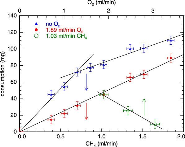
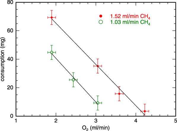
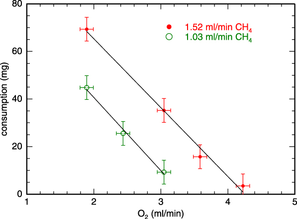
The competing process of re-oxidation of the source material becomes even more prominent when the O2 flow is increased while keeping the CH4 constant. As shown in Fig. 2 (green circles), the consumption decreased further when the O2 flow was increased from 1.89 mL/min to 3.05 mL/min while keeping the CH4 flow constant at 1.03 mL/min. This linear behavior could be observed for different CH4 concentrations (Fig. 3). An increased amount of CH4 increased the overall consumption, as expected. The consumption was also reduced drastically when adding more O2. Here, an O2 flow of 4.23 mL/min compensated almost completely the reduction of the ZnO source powder by a flow of 1.52 mL/min CH4.
Influence of oxygen on the reduction of the source material with 1.52 mL/min (red dots) and 1.03 mL/min (green circles) flow of CH4. The increased amount of O2 increases the re-oxidation of the source material, thus leading to lower consumption.
For the growth of ZnO layers and nanowires, an optimal set of parameters has to be found. Enough oxygen must be added to achieve growth, but should be low enough to not suppress the reduction of the source material.
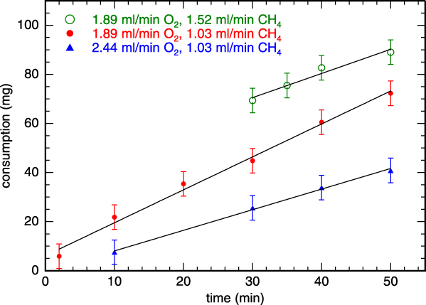
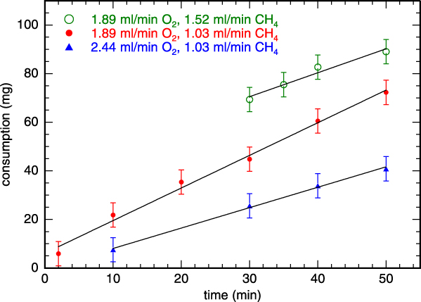
To have control over the resulting thickness of the ZnO layer or the length of the nanowires, a linear time dependence of the process is desirable. As shown in Fig. 4, we performed growth experiments with different parameter sets for several growth times, leading to a linear dependency of the consumption on the process time for all parameter configurations. Starting from the series with 1.89 mL/min O2 and 1.03 mL/min CH4 (red dots), which are typical parameters used in our setup for the growth of ZnO layers, a higher CH4 flux resulted again in higher consumption (green circles). Adding more oxygen instead led to the opposite behavior, i.e., the amount of consumed ZnO powder was decreased by the enhanced re-oxidation of the Zn vapor (blue triangles).
Time dependency of the source material consumption. For different CH4/O2 flows, a linear increase of the consumption with longer growth times was found.
B. Growth of ZnO layers and nanowires
With the method presented, we have successfully grown ZnO layers as well as nanowires on different kinds of substrates. The layers are typically grown at temperatures around 800 °C with a CH4 flux of 1.03 mL/min and an oxygen flux between 1.9 and 6 mL/min. As substrate material, either GaN layers grown on c-sapphire, or c-sapphire with an AlN nucleation layer (both grown by MOVPE) have been used. High resolution X-ray diffraction (HRXRD) and low-temperature PL spectroscopy have confirmed the excellent material quality of the layers grown by our procedure. A comprehensive discussion of the characterization results as well as further details about the layer growth on these substrates have been published earlier. Reference Huber, Madel, Reiser, Bauer and Thonke27
For the growth of ZnO layers on sapphire, a ZnO nucleation layer was deposited on c- and a-plane sapphire substrates as described in the experimental section above. The growth of a closed ZnO layer with crystal quality comparable to the samples on GaN and AlN was only possible on a-plane sapphire. An improved in-plane alignment of c-oriented ZnO on a-plane sapphire was observed before Reference Fons, Iwata, Yamada, Matsubara, Niki, Nakahara, Tanabe and Takasu28 and might be the reason for the higher quality of ZnO layers on this type of substrate compared to c-plane sapphire.
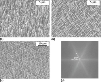
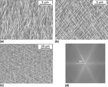
To realize the growth of ZnO nanowires, we increased the CH4 flux to 1.52 mL/min while keeping the O2 flow at a relatively low level (from 1.89 to 3.05 mL/min). This led to a ≈30% higher source material consumption and thus to a higher Zn concentration in the gas phase compared to the layer growth process. At a sample temperature of 830 °C, nanowires were grown both on c- and a-plane sapphire. In Fig. 5 SEM micrographs of the resulting samples are shown. On the a-plane sapphire [Fig. 5(a)], dense nanowires with typical diameters between 50 and 100 nm and uniform length of ≈6 µm were grown, showing no clear lateral orientation. The polycrystalline seed layer led to a random nucleation of the ZnO during the growth process on the a-plane sapphire. Using the same seed layer on c-plane sapphire also resulted in nanowire growth with typical diameters between 50 and 70 nm, but now with clear preferential alignment, as visible in the SEM image recorded with 30° tilt [Fig. 5(b)]. The orientation of the nanowires can be seen even more clearly in the top-view image of the sample, shown in Fig. 5(c). Three preferred growth directions, rotated by an angle of 120° in between, are observable. The Fast Fourier Transformation (FFT) of this SEM micrograph shows an angle of 60° between two adjacent streaks [Fig. 5(d)] corresponding to the 120° orientation of the nanowires. This 3-fold symmetry is commonly attributed to the epitaxial relationship
 ${\left( {0001} \right)_{{\rm{ZnO}}}}\Vert{\left( {10\bar 14} \right)_{{\rm{sapphire}}}}$
, for which the in-plane lattice mismatch is considerably reduced compared to the upright growth along the c-direction of the sapphire.
Reference Kong and Cho29–Reference Weigand, Tveit, Ladam, Holmestad, Grepstad and Weman31
The length of the nanowires is determined by the growth time during which the mixture of CH4 and O2 flows into the system. A growth time of 50 min resulted in wires with ≈10 µm length.
SEM micrograph of ZnO nanowires grown on (a) a-plane sapphire (tilt: 30°), and (b) c-plane sapphire (tilt: 30°). The top-view SEM image (c) of the nanowires on c-plane sapphire shows 3-fold symmetry, which is confirmed by the corresponding Fourier transformed image (d).

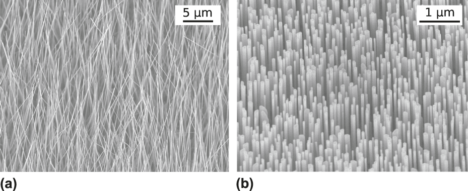
To compare the ZnO nanowires grown by this new growth method with those grown by an established method, nanowires were grown by carbo-thermal CVD as described in the experimental section. Fig. 6 shows the SEM micrographs of the resulting ZnO nanowires on silicon with a thin Au catalyst layer, and on a-plane sapphire. On silicon, very dense, randomly arranged nanowires with a diameter of ≈100 nm are seen. In contrast, the resulting ZnO nanowires on a-plane sapphire are homogeneous in height, whereas the diameters of the nanowires have a broad distribution. A clear orientation of the nanowires in c-direction can be observed, caused by the in-plane alignment given by
 ${\left[ {11\bar 20} \right]_{{\rm{ZnO}}}}\Vert{\left[ {0001} \right]_{{\rm{sapphire}}}}$
.
Reference Fons, Iwata, Yamada, Matsubara, Niki, Nakahara, Tanabe and Takasu28
This c-orientation of the ZnO nanowires was not observable for the growth on a-plane sapphire with CH4 as reducing agent, but the resulting nanowires show a narrower distribution of thinner diameters.
SEM images (tilt: 30°) of ZnO nanowires grown by “classical” carbo-thermal CVD (a) on silicon (111) with a 3 nm thin gold catalyst-layer and (b) on a-plane sapphire with a ZnO seed layer.

C. Optical properties of ZnO nanowires
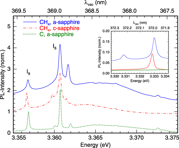
The PL spectra of the ZnO nanowires (Fig. 7), recorded at low temperature (≈5 K), show several sharp emission lines, which all can be assigned to donor-bound-exciton transitions. Both the samples grown with CH4 as reducing agent, as well as the reference sample for which carbon was used, showed similar emission characteristics. The most prominent line in all three spectra is the aluminum-related D0X I6 at 3.3608 eV Reference Meyer, Alves, Hofmann, Kriegseis, Forster, Bertram, Christen, Hoffmann, Straßburg, Dworzak, Haboeck and Rodina32 with a full with of half maximum (FWHM) of 450–500 µeV, followed by the indium-related D0X I9 at 3.3567 eV. Reference Meyer, Alves, Hofmann, Kriegseis, Forster, Bertram, Christen, Hoffmann, Straßburg, Dworzak, Haboeck and Rodina32 While the aluminum incorporation might be caused by the substrate, indium is presumably introduced by residual impurities in the source material.
Low-temperature PL spectra for ZnO nanowires grown on sapphire substrates. For better visualization, the spectra are normalized to the I9 line, and an offset has been added.
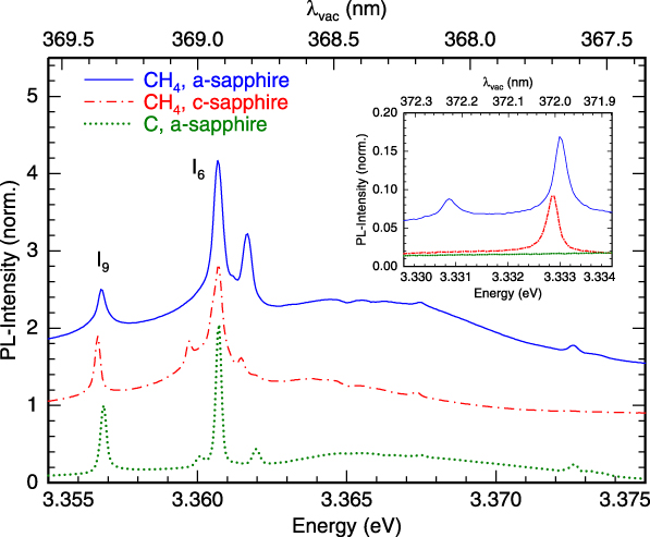
In the inset the lower energy part of the spectra is shown. The line at 3.333 eV is commonly assigned to stacking faults. Reference Schirra, Schneider, Reiser, Prinz, Feneberg, Biskupek, Kaiser, Krill, Thonke and Sauer33 While for both samples grown with CH4 a weak contribution was observable, no defect-related line was found for the nanowires grown with carbon on a-plane sapphire. One reason might be the improved c-plane alignment of the nanowires, which was observable for this type of samples, and which appears to give less rise to misaligned crystal planes.
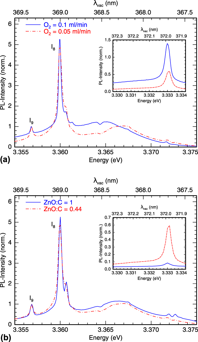
A second series of comparison samples was grown by carbo–thermal CVD on silicon (111) substrates varying the oxygen concentration as well as the ratio of ZnO and graphite powder in the source material. The PL spectra of the first set of samples grown using a ZnO/C powder mixture with a molar ratio of 0.44 is shown in Fig. 8(a). Besides the indium-related D0X I9, which was already observed for the samples using CH4 for reduction, the main contribution at 3.3598 eV corresponds now to the gallium-related D0X Reference Meyer, Alves, Hofmann, Kriegseis, Forster, Bertram, Christen, Hoffmann, Straßburg, Dworzak, Haboeck and Rodina32 (I8, FWHM: 400–500 µeV), which again might be caused by residual impurities in the source material. A variation of the oxygen concentration did not lead to a significant reduction of the defect-related PL around 3.333 eV. However, by changing the molar ratio in the source material to 1, a clear decrease of the defect-related line could be observed, while the line width of the donor-bound-exciton transitions remained comparable [Fig. 8(b)].
Low-temperature (T = 5 K) PL spectra of ZnO nanowires grown on Si(111) substrates (for better visualization, the spectra are normalized to the I9 line). (a) The samples grown with a molar ratio of 0.44 of the ZnO/C source material show a stacking fault related signal around 3.333 eV. (b) By increasing the molar ratio to 1, a significant reduction of this line could be observed (O2 = 0.05 mL/min).
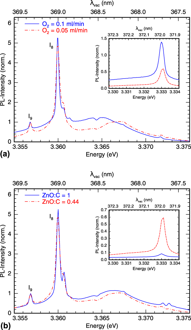
The PL measurements show that both methods resulted in nanowires with equivalent optical properties. Furthermore, the reduced defect-related line at 3.333 eV for the sample with the adjusted source material mixture substantiates the presumption that the amount of Zn atoms in the vapor phase is crucial for successful nanowire growth. This was also observed in the growth using CH4 for reduction, where a higher consumption was necessary to switch from layer to nanowire growth.
IV. CONCLUSIONS
We obtained the growth of ZnO layers and nanowires on different substrate materials using CH4 as reducing precursor in a CVD-based method. Excellent controllability of the source material consumption by this reduction agent was clearly demonstrated. The precise control of the amount of reduced source material, and hence the concentration of Zn atoms in the vapor phase, is crucial for high quality growth of ZnO. The technical design of the process presented leads to a partial re-oxidation of the source material. This has to be taken into account for the optimization of the gas fluxes applied to obtain the optimal II–VI ratio. In addition to high growth rates, a large area of homogeneous growth on the substrate could be achieved. ZnO layers with high crystal quality as well as nanowires were grown both on c- and a-plane sapphire substrates. On c-sapphire, a 3-fold rotational symmetry of the resulting wire tilt was observable. In low-temperature PL spectroscopy the optical properties of the nanowires were investigated, showing several sharp donor-bound exciton transitions and a weak stacking-fault related line, similar to that seen for nanowires grown by more traditional methods.
ACKNOWLEDGMENTS
The authors thank Prof. C. Littler, M. Hocker, M. Lamprecht, and A. Reiser for scientific support.