I. INTRODUCTION
Nanostructured crystalline TiO2 materials have attracted enormous research interest over the last two decades due to the excellent electrochemical, photochemical, and photoelectrochemical performances for potential applications in energy and environmental fields. Reference Hagfeldt and Gratzel1–Reference Ma, Wang, Jia, Chen, Han and Li6 Nanocrystalline TiO2 thin films with large specific surface areas are preferable for application in photovoltaic solar cells, micro-supercapacitors, sensors, self-cleaning windows, and large-area photocatalytic degradation and reduction. However, large-scale and cost-efficient manufacturing has been a significant challenge for commercialization due to the industrial requirements: relatively simple setup, safe and pollution-free processing, low power consumption, and high throughput production. Traditional crystallization processes of metal oxides nanomaterials are initiated by chemical, electrochemical, kinetic, and thermal energies, but these conventional conversion processes require either complex reaction conditions and equipment or processing for long durations with high-energy consumption. Although capable of producing high-quality films, physical and chemical vapor deposition processes, electrochemical methods, and wet chemical processes combined with post thermal annealing do not meet the industrial requirements.
Combining low-cost and scalable processing of organometallic precursor solution deposition with the rapid processing and high-throughput production of industrial-scale pulsed visible light irradiation is one potential pathway to the manufacturing of nanostructured crystalline metal oxides thin films. Reference Nakjima, Shinoda and Tsuchiya7–Reference Kang, Ryu, Kim and Hahn11 Normally, photosensitive materials could absorb pulsed light to generate heat through non-radiative energy dissipation and exothermic photochemical reaction. Photoinitiated decomposition of photosensitive organometallic precursor would open a new path to achieve crystalline metal oxides once the generated heat supplies enough activation energy for oxidation and crystallization of the metallic component. There are 3 mechanisms for pulsed light irradiation to rapidly process materials: (i) for one-dimensional light-absorbing nanomaterials, the small structures cannot efficiently dissipate the absorbed energy and hence the absorbance of light results in near instantaneous high temperatures, Reference Ajayan, Terrones, Guardia, Huc, Grobert, Wei, Lezec, Ramanath and Ebbesen12–Reference Wang, Yao, Chan and Zhang14 (ii) for traditional polymer films and bulks, similar to ultraviolet (UV) curing, a radiation-induced polymerization occurs, (iii) for metals and inorganic nonmetallic materials showing high attenuation of light, the large photothermal conversion rate results in internal heating of the materials. Pulsed light irradiation would supply light energy to initiate the photodecomposition and photothermal post-treatment.
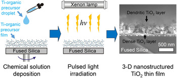
In this work, we demonstrate a novel approach for the instantaneous photoinitiated synthesis of TiO2 thin films with a three-dimensional (3-D) nanostructure through pulsed white light irradiation of photosensitive Ti-organic precursor films made by chemical solution deposition (see Fig. 1). To minimize the effect of substrate heating on the precursor film under pulsed light irradiation, transparent fused silica glass substrates (1.5 mm thickness) were used for the film processing. Precursor solutions of Ti diisopropoxide bis-acetylacetonate (Ti-acac) dissolved in isopropanol were spin-coated on the silica glass substrates to form films for irradiation. Instantaneous photoinitiated synthesis combined with subsequent in situ pulsed photothermal treatment was performed through a continuous pulsed light irradiation implemented by the PulseForge 1300 photonic curing system. The microstructures of the thin films were characterized and analyzed to demonstrate the approach, and mechanisms are discussed.
Schematic of instantaneous photoinitiated synthesis of 3-D nanostructured TiO2 thin film.

II. EXPERIMENTAL
A titanium diisopropoxide bis(acetylacetonate) (Ti-acac) solution (75 wt% in isopropanol, Sigma-Aldrich, St. Louis, Missouri) was diluted to further low concentrations in isopropanol for the deposition of Ti-acac precursor films. The Ti-acac precursor films were deposited on fused silica (1-inch diameter circle, Ted Pella, Redding, California) substrates by a spin-coating process at 500 r.p.m for 10 s and 3500 r.p.m for 20 s. The substrates were cleaned prior to coating by sequential ultrasonic treatment in ethanol, acetone, and deionized water for 5 min before drying by nitrogen blowing, respectively. 2 droplets of 5 μL precursor solution were drop-casted on the substrate for the spin coating process. The as-spin-coated precursor films were irradiated by using an industrial-scale photonic curing system (PulseForge 1300; NovaCentrix Corp., Austin, Texas). The parameters of pulsed light irradiation including lamp discharge voltage and pulse train of a pulsed Xe lamp were controlled by a computer and the energy density of a pulse sequence onto the samples was measured by an integrated bolometer. The parameters used for all films are voltage: 650 V, envelope width: 1930 μs, μpulses: 8, fire rate: 1.2 Hz, pulse fluence: 7.7 J/cm2, total pulses: 200. A temperature simulation was performed by the integrated program for the surface of the system (film/substrate/aluminum test bed). The irradiated film samples were plasma cleaned at 29.6 W RF power to remove its carbon materials using a plasma cleaner (PDC-001; Harrick Plasma, Ithaca, New York). The whole process was carried out in ambient condition and at room temperature.
The surface and cross section morphologies of films were observed by field-emission scanning electron microscopy (Hitachi S-4800, Hitachi Corp., Tokyo, Japan). The films’ surfaces were scraped off from the substrate for transmission electron microscopy (TEM), high-resolution transmission electron microscopy (HRTEM), and selected area electron diffraction (SAED) characterizations performed by using FEI’s TECNAI G2 F30 FEG TEM (FEI Company, Hillsboro, Oregon) at the acceleration voltage of 300 kV. The optical transmission measurement of precursor solutions and irradiated films was conducted using a UV–visible spectrophotometer (Shimadzu UV-1700, Shimadzu Corp., Kyoto, Japan). NovaCentrix Corp. supplied the spectra of a xenon lamp in the PulseForge photonic curing system. Raman spectra were recorded using a DXR Raman microscope (Thermo Scientific, Waltham, Massachusetts) with a 532 nm laser as the excitation source and spot size of 2 μm. X-ray photoelectron spectroscopy (XPS) measurements were performed by using a VG MultiLab 2000 system with a monochromatic Al Kα X-ray source (Thermo Scientific). A charge neutralizer was used to neutralize the charge effect and a 0.05 eV scan step energy was used for the core scan. The films’ surfaces were in situ cleaned by Ar+ ion bombardment for 3 min in the vacuum chamber before the XPS measurement. After Shirley-type background subtraction, the raw XPS spectra were fitted for the quantification and hybridization analysis. The binding energy shifts of the C1s and Ti2p core-levels due to relative surface charging were corrected by using the C–C level at 285.0 eV and Ti4+(–O)2p 3/2 level at 458.5 eV as the internal standards, respectively. All of the operations were carried out at room temperature.
III. RESULTS AND DISCUSSION
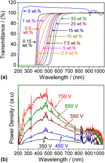
The UV–visible transmission spectra of Ti-acac precursor solutions with various concentrations show a concentration dependent light absorption range, as shown in Fig. 2(a). With air as a reference scan, pure isopropanol solvent (0 wt% Ti-acac solution) shows transmittance over 100% and a UV cutoff at 200 nm, indicating isopropanol absorbs negligible light energy from the lamp source. All of the Ti-acac precursor solutions show a sharp cutoff in the visible or UV region. The light source of a xenon lamp emits mostly as visible light, and its spectra are shown in Fig. 2(b). The wave length range of the light source is from 200 to 1100 nm, and the visible lights (390–780 nm) make up >60% light energy while the UV lights make up 20–30%. The absorption edge of precursor solutions shows an apparent blueshift as Ti-acac concentration decreases, indicating that solutions in a lower concentration absorb less visible light and light energy from the light source. The Ti-acac precursor solution needs to be diluted to low concentrations (<30 wt%) in isopropanol solutions to avoid the rapid hydrolysis from ambient humidity. We selected the Ti-acac precursor solution with a moderate concentration of 10 wt% to demonstrate the process. The pulsed white light irradiation was carried out with a moderate shot fluence of 7.7 J/cm2.
(a) UV–visible transmission spectra of Ti-acac precursor solutions with various concentrations from 0 wt% (pure isopropanol) to 50 wt%. (b) Spectra of xenon lamp in the PulseForge photonic curing system.

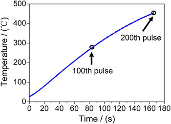
A fused silica glass with a thickness of 4 mm is placed between the aluminum stage (6 mm) and the 1.5 mm thick fused silica substrate to prevent direct heating of the sample from the aluminum stage with a gradual rise in temperature during processsing. The surface temperature simulation of the fused silica substrate under 200 pulses of light irradiation is shown in Fig. 3. The simulated temperature on the surface of fused silica substrate rises with increasing pulse count, or irradiation time, then reaching 280 °C after the 100th pulse (84 s) and rises to 460 °C after 200 pulses (166 s). The crystallization temperature of TiO2 is considered above 350 °C. To determine if sample heating caused crystallization, a spin-coated 10 wt% Ti-acac (Ti-10) precursor film was baked at 150 °C for 20 min to form an amorphous titanium oxide thin film that was then irradiated with 200 pulses. This irradiated sample showed amorphous character as shown in Fig. S1. A rapid thermal annealing (RTA) treatment of the spin-coated Ti-10 precursor film was performed in a RTA furnace (with a IR lamp) from room temperature to 500 °C in 180 s. The RTA-treated film also exhibited amorphous character as shown in Fig. S2. From this it is concluded that pulsed light irradiation with the parameters described above does not work as rapid heat treatment for thermal crystallization of the amorphous titanium oxide films and hence would not obviously affect the film processing as a traditional heat treatment.
Temperature simulation on the surface of fused silica substrate under the experimental setting.

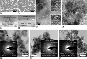
Subsequently, we processed the as-spin-coated Ti-10 liquid precursor films by pulsed light irradiation. The SEM surface and cross-sectional morphologies of the spin-coated Ti-10 films after 1 pulse and 100 pulses irradiation are shown in Figs. 4(a)–4(d). The liquid Ti-10 precursor film was transformed into a 3-D nanostructured thin film after the first pulse irradiation [Figs. 4(a) and 4(c)]. As-synthesized Ti-10 thin film consisted of a relatively flat and dense bottom layer with a thickness of about 60–80 nm on the substrate and a porous top layer composed of many dendritic islands with a maximum height of about 1 µm above the bottom layer which correspond to the dark continuous areas and the bright discrete regions shown in Figs. 4(a)–4(b), respectively. TEM images and SAED patterns of the Ti-10 films after 1 pulse, 100 pulses, and 200 pulses irradiation are shown in Figs. 4(g)–4(i). The indexed diffraction patterns in Fig. 4(g) demonstrate that the 1-pulse irradiated Ti-10 film contains the polycrystalline TiO2 components with mixed phases of anatase and rutile despite poor crystalline quality as shown by the diffuse ring patterns. The clear SAED patterns with indexes in Fig. 4(h) indicate that the 100-pulses irradiated film is well-crystallized and has mixed phases of TiO2. The more prominent SAED patterns shown in Fig. 4(i) indicate that 200 pulses irradiation resulted in better crystal quality of TiO2 thin film. The HRTEM images shown in Figs. 4(e)–4(f) further confirm that the 100- and 200-pulses irradiated Ti-10 films are well-crystallized nanocrystalline TiO2 thin films with a grain size around 10–30 nm. As shown in Fig. S3, the high magnification SEM images of the cross-sectional morphology with a tilt angle and the surface morphology of the 100 pulses-irradiated Ti-10 film confirm that the dense bottom layer is pore-free and with a grain size around 10–30 nm. Combining SEM morphologies with TEM images, it is clear that the 50–100 nm nanoparticles composed of 10–30 nm TiO2 nanograins self-assembled into the 3-D nanostructured thin films. The subsequent hundreds of pulses remarkably improved the crystalline quality without obviously affecting on the grain size and morphology of the films. In addition, the polycrystalline TiO2 thin films should not have preferential orientation from the HRTEM and SAED results.
SEM (a), (b) surface morphologies and (c), (d) cross-sectional images of Ti-10 films on fused silica substrates after (a), (c) 1 pulse and (b), (d) 100 pulses irradiation. High-resolution TEM lattice images of the Ti-10 film after (e) 100 pulses and (f) 200 pulses irradiation. TEM images with inserted SAED patterns of the Ti-10 films after (g) 1 pulse, (h) 100 pulses and (i) 200 pulses of irradiation. A and R represent anatase and rutile, respectively.

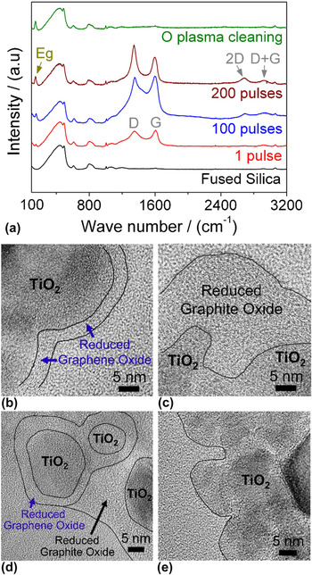
An audible photoacoustic phenomenon was observed during the first pulse irradiation of the spin-coated Ti-10 precursor film, and the yellow liquid precursor film transformed into a transparent light-grey solid thin film after the irradiation, implying that a pulsed photoinitiated decomposition accompanied by a high-temperature chemical reaction process that took place in Ti-acac molecules, Reference Chen and Diebold15 and resulted in carbon-related materials. Figure 5(a) shows the Raman spectra of the Ti-10 thin films after 1 pulse, 100 pulses, and 200 pulses irradiation, and further 1-h oxygen plasma cleaning. The D band (1350 cm−1) and G band (1580 cm−1) relate to the first-order scattering of sp 2 carbons by defects that broke the basic symmetry of the graphite sheet and the vibration in all sp 2 carbon materials, Reference Dresselhaus, Jorio, Hofmann, Dresselhaus and Saito16 respectively. The appearance of the 2D band presents the existence of reduced graphene oxides. It indicates that the carbon components resulted from the pulsed photodecomposition of Ti-acac molecules that mainly existed in the form of graphitic oxides. The increase in intensity ratio of D versus G and the sharper D peak indicate an evident reduction of graphitic oxides as an increasing pulse number of light irradiation due to the photothermal effect as well as photocatalytic TiO2. Reference Cote, Cruz-Silva and Huang17–Reference Bell, Ng, Du, Coster, Smith and Amal22 The peak located at 150 cm−1 corresponding to the E g mode of anatase TiO2 was observed in all the films. Furthermore, all peaks corresponding to the carbon materials disappeared after 1-h oxygen plasma cleaning, indicating that the carbon components in the films can be easily and completely removed to obtain pure TiO2 thin films. The HRTEM images in Figs. 5(b)–5(e) clearly show that the reduced graphitic oxides, including reduced graphene and graphite oxides, coat the TiO2 nanograins in the 100- and 200-pulses irradiated thin films and have been completely removed from the film after subsequent 1-h oxygen plasma cleaning. It is noteworthy that reduced graphitic oxides previously have been added into the TiO2 nanocrystalline materials to increase the electrical conductivity and the light absorption for enhanced performance in photocatalytic and photovoltaic applications. Reference Bell, Ng, Du, Coster, Smith and Amal22,Reference Wang, Ball, Barea, Abate, Alexander-Webber, Huang, Saliba, Mora-Sero, Bisquert, Snaith and Nicholas23
(a) Raman spectra of the Ti-10 films after 1 pulse, 100 pulses, and 200 pulses irradiation and further 1-h oxygen plasma cleaning. HRTEM images of the Ti-10 thin film after (b), (c) 100 pulses and (d) 200 pulses irradiation, and (e) further oxygen plasma cleaning.

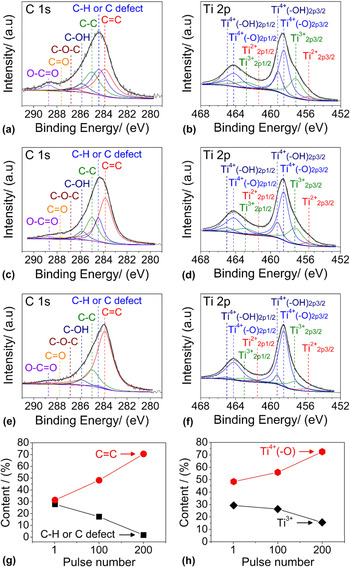
We also performed the XPS study on the surface chemical states of 3-D nanostructured TiO2 thin films. The C1s and Ti2p core-level spectra of the Ti-10 thin films after 1 pulse, 100 pulses, and 200 pulses irradiation are shown in Figs. 6(a)–6(f). After deconvolution and Shirley background fitting, each raw C1s spectrum and Ti2p spectrum fit well with seven chemical carbon-related environments Reference Hong, Song, Sul and Cho24,Reference Koinuma, Tateishi, Hatakeyama, Miyamoto, Ogata, Funatsu, Taniguchi and Matsumoto25 and four chemical states of Ti ion. Reference Sayers and Armstrong26 The area fractions of C1s and Ti2p peaks are shown in Tables SI and SII, respectively. The content of C–H or C defect and O–C=O relating to graphitic oxides remarkably decreases while that of C=C significantly increases as increasing pulse number from 1 to 200, suggesting that the original graphitic oxides were evidently reduced under continuous pulsed light irradiation. The content of Ti4+ (–O) peak increases while that of Ti3+ decreases remarkably as increasing the pulse number, indicating that the crystalline quality of TiO2 is markedly improved by the subsequent pulsed light irradiation, which is in agreement with the TEM and SAED analysis results.
XPS core-level spectra of (a), (c), (e) C1s and (b), (d), (f) Ti2p for the Ti-10 film after (a), (b) 1 pulse, (c), (d) 100 pulses and (e), (f) 200 pulses irradiation. Curves of (g) C–H or C defect, C=C contents versus pulse numbers and (h) Ti3+, Ti4+ (–O) contents versus pulse numbers.

According to the audible photoacoustic phenomenon and the resulting graphitic oxides from the pulsed photoinitiated decomposition of the Ti-acac precursor film, it is believed that the photodecomposition is a violent and complex process accompanied by high-temperature chemical reactions as well as a large thermal expansion of the body due to the pulsed conversion of absorbed optical radiation to heat. Reference Chen and Diebold15 The high-temperature process resulted in the instantaneous oxidation and crystallization of TiO2 nanograins while the thermal expansion led to the instantaneous self-assembly of 3-D nanostructure with a top layer of dendritic islands and the dense bottom layer due to the surface tension constraint of the substrate. Normally the characteristic absorption of light is required for organometallics to activate the photochemical decomposition that prefers to organic intermediate products rather than the instantaneous formation of graphitic oxides or graphitized carbon materials that require high-temperature circumstance. As shown in Fig. 2(a), Ti-acac precursor solutions do not indicate any distinguished characteristic absorption but exhibit a wide absorption range from visible light to UV light, suggesting that Ti-acac molecules can absorb lots of pulsed light energy that is converted into heat to initiate the photodecomposition process. We believe that it is the pulsed photoinitiated pyrolysis that makes preliminary organic decomposition products transform into graphitic oxides instantaneously through complex photo-physical and -chemical processes due to the instant high temperature.
The Ti-acac precursor solution in a higher concentration absorbs more visible light and light energy from the light source. It was determined that there are energy thresholds needed for the pyrolysis to occur. At 10 wt% a fluence of 4.5 J/cm2 was necessary while at 5 wt% the fluence had to be at least 6 J/cm2. In addition, at 1 wt% it could not occur even the fluence is above 10 J/cm2. Accordingly, the irradiated precursor films without pyrolysis occurring just transformed into amorphous dense thin films that could not be crystallized by the 200 pulses irradiation. Examining the concentration-dependent absorption of pulsed light energy for the Ti-acac precursor solutions, it is suggested that a critical projected area density of Ti-acac molecules that absorbed pulsed light energy is necessary to initiate the pyrolysis process. Pulsed photothermal energy conversion only initiates pyrolysis if enough Ti-organic molecules absorb sufficient energy.
It is well known that TiO2 shows very low attenuation of light and becomes an effective UV absorber when the grain size is below 100 nm but the penetration depth of UV on crystalline TiO2 surface is only around ten nanometers. Reference Jellison, Boatner, Budai, Jeong and Norton27,Reference Krylova and Na28 It is hard for nanocrystalline TiO2 thin film to achieve effective internal heating under pulsed light irradiation through traditional photothermal conversion based on light absorption. For TiO2, the heat could be generated through both the non-radiative recombination of photogenerated electrons and holes and the absorption of high energetic photons with a wave length below 300 nm, the latter only affects the shallow surface of TiO2 thin films due to the small penetration depth. It is believed that the heat generated by the recombination of photogenerated electrons and holes in the TiO2 nanograins, coupled with inefficient heat dissipation due to the low thermal conductivity of 10–30 nm TiO2 grains, Reference Kim, Kim, Cho, Kim, Lee and Kim29,Reference Fang, Reitz, Brezesinski, Nemanick, Kang, Tolbert and Pilon30 supplies enough thermodynamic driving force to rapidly improve the crystalline quality of TiO2 thin films despite its very low attenuation of light.
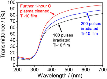
The elemental analysis from the XPS data indicates that the carbon content is around 22 atomic percent in the films. As shown in Fig. 7, the difference in transmittance is around 15% on the visible light region between the 100 pulses-irradiated Ti-10 films and the film after further oxygen plasma cleaning, indicating that the graphitic oxides only absorb a small part of pulsed light energy to generate heat. On the other hand, both the light absorption and photocatalytic reduction of graphitic oxides inevitably reduce the efficiency in recombination of photogenerated electrons and holes and hence reduce the generated heat. We believe that the original and reduced graphitic oxides do not contribute obvious heat for the improvement of the crystalline quality of TiO2 thin films.
UV–vis transmission spectra of the Ti-10 films after 100 and 200 pulses irradiation, and further 1-h oxygen plasma cleaning.

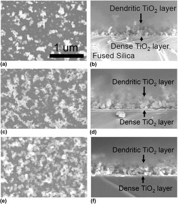
The easy control in the 3-D surface nanostructure of the thin films is significant for both of industrial manufacturing and practical device applications in energy and environmental fields. The precursor films spin-coated by 15 wt% Ti-acac (Ti-15) and 25 wt% Ti-acac (Ti-25) precursor solutions were irradiated for a comparison with irradiated Ti-10 films. As shown in Figs. 8(a)–8(f), it is clearly observed that as increasing concentration of the precursor solution, the density of dendritic islands (bright regions on surface morphologies) remarkably increased and the dendritic top layer transformed from isolated islands into a 3-D network with bridge formation between nanoparticles of dendritic islands. All the films consist of a 60–80 nm thickness dense bottom layer and a dendritic top layer with a height range from several hundreds of nanometer to about 1 μm. It is believed that the more Ti-acac molecules in the precursor films absorb pulsed light energy to participate in the photoinitiated pyrolysis process, the more complex 3-D nanostructure of dendritic top layer forms. Apparently, the projected area density of Ti-acac molecules in the as-spin-coated precursor films, being increased by increasing either the concentration of precursor solution, can be easily adjusted to control the surface nanostructure of the thin films.
SEM surface and cross-sectional morphologies of (a), (b) Ti-10 thin film, (c), (d) Ti-15 (15 wt% Ti-acac) thin film and (e), (f) Ti-25 (25 wt% Ti-acac) thin films on fused silica substrates after 100 pulses irradiation. Pictures (a)–(f) have the same scale bar.

IV. CONCLUSION
To summarize, we demonstrated a novel approach to the instantaneous (milliseconds) photoinitiated synthesis of 3-D nanostructured thin films with mixed phases of rutile and anatase TiO2 through pulsed photoinitiated pyrolysis accompanied by instantaneous self-assembly and crystallization processes, which was achieved through pulsed white light irradiation (xenon flash lamp, pulse width of 1.93 ms, fluence of 7.7 J/cm2, and frequency of 1.2 Hz) of photosensitive Ti-acac precursor films made by chemical solution deposition. Once enough molecules absorbed sufficient pulsed light energy to achieve sufficient photothermal energy conversion, the pulsed photoinitiated pyrolysis process of precursor films occurred to result in graphitic oxides coated TiO2 nanograins. The instantaneously self-assembled 3-D nanostructure consists of a dense bottom layer and a controllable dendritic top layer that transformed into a 3-D network from isolated islands as increasing the projected area density of light-absorbing Ti-acac molecules in the precursor film. Subsequent pulses rapidly (within a couple of minutes) improved the crystalline quality of nanocrystalline TiO2 thin films and led to the reduction of the graphitic oxides. The non-radiative recombination of photogenerated electrons and holes, coupled with inefficient heat dissipation due to low thermal conductivity resulted from 10 to 30 nm nanograin size and thin structure of the films, generated enough heat to provide thermodynamic driving force for rapid improvement of the crystalline quality despite the very low attenuation of light. The further oxygen plasma cleaning can completely remove the carbon materials in the films. The instantaneous photoinitiated synthesis combined with in situ pulsed photothermal treatment achieved through pulsed light irradiation supplies a straightforward and scalable technology to achieve the low-cost and high-throughput manufacturing of nanostructured metal oxides thin films with a large specific surface area for energy and environmental applications.
Supplementary Material
To view supplementary material for this article, please visit https://doi.org/10.1557/jmr.2017.139.