I. INTRODUCTION
The 7 GHz unlicensed frequency band around 60 GHz provides the possibility of high throughput wireless data communication like Wireless Local Area Network (WLAN) or Wireless Personal Area Network (WPAN) up to several Gbit per second. Currently, different 60 GHz implementations based on III/V technologies, silicon bipolar, and Bipolar Complementary Metal Oxide Semiconductor (BiCMOS) have been reported. However, in heterodyne systems [Reference Floyd1–Reference Grass3], the chip-external circuitry is often complicated and costly since IF filtering is required. The off-chip components can be reduced to a minimum using a homodyne concept [Reference Wang4–Reference Marcu6], but non-idealities of the different building blocks have to be overcome, since accurate and precise circuit performance is difficult to achieve at the high operating frequency of 60 GHz. Despite these challenges, the problems have been overcome in mobile communication systems operating up to frequencies of 6 GHz. The goal of this work was to develop and implement a similar approach and evaluate the circuit characteristic. The 60 GHz upconverter and downconverter have been described separately in [Reference Forstner, Ortner and Verweyen7, Reference Ortner, Forstner and Verweyen8], respectively.
II. TECHNOLOGY
The chip is fabricated in Infineon's automotive-qualified B7HF200 SiGe:C bipolar technology which is based on the process technology presented in [Reference Böck9]. The transistors have a double-polysilicon self-aligned emitter–base configuration with an effective emitter width of 0.18 µm. The SiGe:C base of the transistors has been implemented by selective epitaxial growth. The NPN transistor exhibits a monocrystalline emitter contact in the active transistor region without any interfacial native oxide. The process provides a transit frequency f T and a maximum oscillation frequency f MAX of more than 200 GHz, the ring oscillator gate delay amounts to 3.7 ps. The technology provides four copper metallization layers, two different types of polysilicon resistors, a TaN thin film resistor, and an MIM capacitor.
III. CIRCUIT ARCHITECTURE
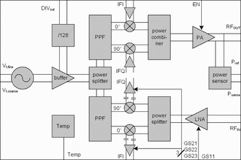
The overall block diagram of the homodyne transceiver is shown in Fig. 1. Superheterodyne architectures are widely used and provide good LO to RF suppression, weak TX carrier feedthrough, and the quadrature phase generation at IF frequencies is easier. However, image and IF filtering is needed, multiple LO frequencies exist and spurs can occur. In contrast, the homodyne or direct conversion architecture is simpler, no image or IF filtering is needed and one single LO frequency generates fewer spurs. These advantages are at the cost of a reduced LO to RF suppression, higher TX feedthrough, and a less precise quadrature phase generation at the high operating frequency of 60 GHz.
Overall block diagram of the transceiver chip.

A fundamental 60 GHz VCO is used for LO signal generation. A buffer amplifier isolates the oscillator core from the rest of the circuit. To ease the frequency synchronization, a fixed divide-by-128 frequency divider has been implemented. The LO signal is split by a passive power divider and polyphase filters are used to provide the quadrature phases for the Gilbert-based up- and downconversion mixers. The differential TX baseband signals are amplified, upconverted, and summed up using an active in-phase signal combiner before the RF signal is amplified by a Class-AB power amplifier and finally fed to the RF output pads of the chip. The RX signal is amplified by the Low Noise Amplifier (LNA), split by a passive power divider and fed to the downconversion mixers. After downconversion, the AC-coupled baseband signals are amplified using a programmable gain amplifier (PGA). A temperature sensor and an RF power sensor complete the circuit. On-chip RF interconnects and impedance transformations are realized by microstrip transmission lines (TRLs) with the top metal 4 metallization layer being used as a signal line and metal 2 as a reference ground. One common supply of 3.3 V is used for all different building blocks of the transceiver.
IV. CIRCUIT DESIGN
A) 60 GHz signal generation
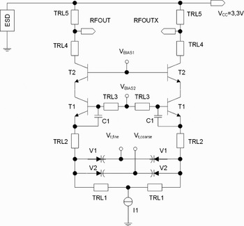
The voltage-controlled oscillator (Fig. 2) is based on a differential Colpitts topology similar to [Reference Li, Rein, Suttorp and Böck10]. In order to achieve low phase noise and sufficient tuning range over process and temperature variations, the circuit uses differential high-Q varactors (V1, V2) available in the B7HF200 process. To ease the implementation of a Phase Locked Loop (PLL), separate coarse and fine tuning inputs with different tuning sensitivities are provided. With this option, the VCO can be pre-adjusted by applying an appropriate tuning voltage to the coarse-tune input (e.g. filtered DAC output) and the PLL is closed using the fine-tune input with less tuning slope. This can help to avoid degradation of the inherent VCO phase noise by parasitic noise injection. To widen the tuning range, a metal–insulator–metal capacitor (C1) is placed in parallel to the base–emitter diffusion capacitance of transistors T1, which is part of the tank circuit. The oscillator covers the full frequency range from 57 to 64 GHz, draws a current of 42 mA, and is buffered from the following circuit using a stacked common base stage T2.
Simplified schematic diagram of the 60 GHz voltage-controlled oscillator.

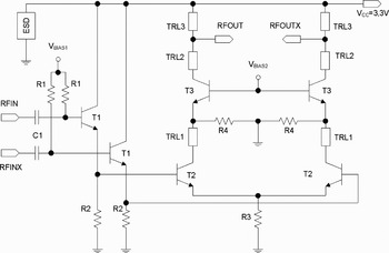
The buffer, shown in Fig. 3, consists of an emitter-follower pair (T1), an emitter-coupled transadmittance stage (T2), and a differential grounded-base stage (T3), additionally biased by a constant current (R4). The output of T3 is matched to the 70 Ω load by TRL2 and TRL3. Under nominal conditions, the buffer provides a differential output power of 13 dBm and draws a current of 61 mA. Its output drives the input of a differential rat-race-type power splitter that delivers the LO signal for the following RC polyphase filters, which generate the quadrature output for the up- and downconversion mixers.
Simplified schematic diagram of the buffer amplifier.

There are basically two options for I/Q signal generation with RC polyphase filters [Reference Notten and Veenstra11]. One approach exhibits a correct wideband amplitude balance, but a correct quadrature phase relationship only at the center frequency. The characteristic of the second approach is vice versa. Since amplitude fluctuations at the LO input of a mixer are reduced by the inherent AM suppression of the LO buffer, the latter approach has been chosen. The tantalum-nitride filter resistor values were initially chosen to be 50 Ω, resulting in a capacitor value of 53 fF. Final optimization of the filter component values and physical size was based on simulations of the extracted layout. The simulated transfer loss of the final filter is 5.2 dB at the center frequency of 60 GHz and the maximum absolute phase variation is 0.4° from 57 to 64 GHz.
To ease the PLL-based synchronization to an external reference frequency, a divide-by-128 frequency divider is integrated. Because of its high maximum operating frequency, wide bandwidth and low power consumption, a regenerative divider is used in the first stage. All following stages are based on Emitter Coupled Logic (ECL) and Current Mode Logic (CML) master–slave flip-flops.
The transceiver chip also contains a temperature sensor for monitoring purposes. It is based on the ΔVBE of NPN transistors operated at different current densities.
B) Gilbert-based upconversion mixer
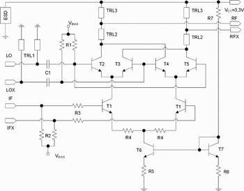
The two upconversion mixers are based on a Gilbert-type topology as shown in Fig. 4. The differential 100 Ω IF input is DC coupled, the transconductance stage T1 converts the input voltage to an output current. The typ. small signal gain of the upconverter is 0.5 dB, adjusted by the emitter degeneration resistors R4 that linearize the upconversion characteristic. At the maximum IF input voltage swing of 200 mVpp, originating from a D/A converter, the upconversion mixer is compressed less than 0.1 dB. A minimum LO signal drive of 0 dBm is required, which is fed to the switching transistors T2–T5 via the input matching network TRL1 and C1. It transforms the input impedance to 100 Ω. At the 60 GHz RF output of the upconverter, microstrip lines TRL2 and TRL3 accompany the output transformation. Since no intentional bandwidth limitation has been implemented on the chip, the mixer offers a −3 dB modulation bandwidth from DC to 10 GHz. The Gilbert-mixer core draws a current of 13.4 mA and the complete upconverter consumes 17.1 mA from the 3.3 V supply.
Simplified schematic of the upconversion mixer.

C) Active in-phase signal combiner
In order to sum up the output carriers of the individual modulators, an active in-phase power combiner has been designed, which is shown in Fig. 5. With respect to a passive structure, the active combiner increases the linear output power of the individual modulators and simultaneously isolates their outputs, which is beneficial in terms of upconversion linearity.
Simplified schematic of the active in-phase signal combiner.

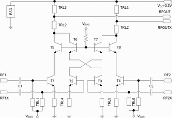
Adopting inductive emitter degeneration by TRL4 and TRL5 on the CE input stages T1/T2 and T3/T4, the overall gain is adjusted to 10 dB. TRL4 and TRL5 series feedback also increases the real part of the input impedance and eases input matching to the 100 Ω differential source. The individual output currents of T1–T4 are summed up by segmented common base stages T5–T8 and their outputs are matched to 100 Ω using TRL2 and TRL3. The typical simulated isolation of the two individual inputs is 30 dB. The circuit is biased at 30 mA and provides an output referred 1 dB compression point of 11.1 dBm. At the maximum PA input drive of approximately +3 dBm, the circuit is compressed by only 0.1 dB and hence provides enough linear drive power.
D) Power amplifier
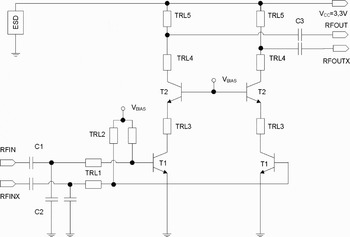
After baseband upconversion and signal combination, the 60 GHz carrier is amplified by a linear Class-AB cascode power amplifier as shown in Fig. 6. Common emitter transistors T1 are biased by a low ohmic current mirror that enables linearization, since the DC current is allowed to increase with rising signal drive. Broadband input matching is done using a shunt inductance TRL2 and a following low-pass match based on TRL1 and C2 (75 fF). C1 acts as a DC block and the output match to the differential 100 Ω load is realized by TRL4 and TRL5. Common emitter transistors T1 operate at the maximum current density of 5 mA/μm2. To ease output matching, common base transistors T2 operate at a slightly lower current density. The PA draws a current of 85 mA from the 3.3 V supply and provides a small-signal gain of 15.7 dB at 60 GHz under nominal operating conditions. The simulated 1 dB compression point is +16 dBm at a collector efficiency of 14% and the simulated saturated output power is 18 dBm. To provide a measure for the output power of the PA, a sensor has been implemented (Fig. 1). The full-wave rectifier is weakly capacitively coupled to the differential PA output and has a linear dynamic range of more than 30 dB.
Simplified schematic of the power amplifier.

E) Low-noise amplifier
To achieve sufficiently high LNA gain in order to overcome the signal loss of the passive power splitter and minimize the contribution of mixer noise to the overall noise figure, three common-emitter stages are used. For power saving reasons, the current of the third stage was reused in the first and second stages. Furthermore, the second stage offers two gain steps. Switching the second stage has the advantage that the input as well as the output remain well matched in both gain step modes and the more complex gain step circuitry has less influence on noise figure.
The current is distributed in a way that the first stage (LNA1) draws a current of 3.5 mA and the second stage (LNA2) draws a current of 7 mA in high-gain mode and 1.8 mA in low-gain mode. This results in a current of 10.5 mA (5.3 mA in low-gain mode) through the third stage (LNA3). The collector voltage of 1.28 V for the first two stages is regulated by a linear regulator. The overall current consumption of the LNA including bias circuitry is about 11 mA from a 3.3 V supply. The simplified schematic of the LNA is shown in Fig. 7. Interstage matching as well as input and output matching to 100 Ω is achieved with the transmission lines TRL1–TRL10. The common-emitter transistors T1, T2, and T4 of the first two stages are biased with current mirrors (not shown). To improve matching of the current mirrors, emitter-degeneration resistors are used (R1, R3, and R5). Transistors T2 and T3 form the high-gain stage of stage two while transistors T4 and T5 form the low-gain stage.
Simplified schematic of the low noise amplifier.

In order to increase gain and reverse isolation, the second stage (LNA2) is neutralized by cross-coupling additional transistors (T3, T5) with the main transistors (T2, T4). Since neutralization also reduces the bandwidth, it was only done once in the second stage. Gain reduction in the low-gain stage is obtained by current reduction as well as resistive emitter degeneration (R6). The resistor R8 together with the capacitance C6 improves common-mode suppression and stability. The LNA has a gain of 17 and 1 dB in high-gain- and low-gain modes, respectively. The noise figure is about 5 dB in high-gain mode and the simulated high-/ low-gain mode input compression points are −16 and −10 dBm.
F) Baseband amplifier
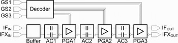
In homodyne receivers, LO self-mixing can cause significant DC-offsets which could compress or even saturate a DC-coupled high-gain IF amplifier. Hence DC-offset removal is desirable. However, an on-chip AC coupling stage with a lower cut-off frequency as low as possible is needed, otherwise receive signal information content is lost. The block diagram of the baseband amplifier is shown in Fig. 8.
Block diagram of the baseband amplifier.

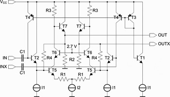
To remove DC-offsets, also introduced by mismatches of the differential amplifier, each PGA is preceded by an AC-coupling stage as shown in Fig. 9.
Simplified schematic of the AC-coupling stage.

In order to achieve a lower cut-off frequency in the kilohertz range as well as an upper cut-off frequency close to 1 GHz with a moderately sized AC-coupling capacitor (C1 = 10 pF), a high-ohmic and low-capacitive biasing for the emitter-follower T2 is needed. This is provided by the current mirror T3/T4, for which T1 acts as a reference path. To avoid stability issues, the cascode amplifier T5/T6 isolates the transistor T2 from the following PGA. Moreover, it shifts the DC-level to provide the biasing for the PGA input transistor. The PGA consists of resistively emitter-degenerated differential amplifiers, which offer high bandwidth and high linearity. The output driver of PGA3 is designed to drive a 100 Ω load. The PGA draws a current of 29.5 mA from a 3.3 V supply and exhibits a maximum voltage gain of 42 dB.
V. MEASURED RESULTS
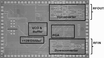
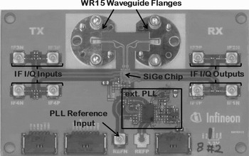
The final chip, shown in Fig. 10, has been characterized using an evaluation board as depicted in Fig. 11.
Chip photo of the transceiver; the chip dimensions are 3.25 × 2.1 mm2.

Photo of the evaluation board of the 60 GHz transceiver chip.

The 360 µm thick chip is attached into a cavity of a 5 mil Taconic TLE-95-0052 substrate and the differential RF output is bonded to the PCB using lateral wedge–wedge bonds. Bondwire impedance compensation on the TX out- and RX input is done by a λ/4 transformer and after a distance of 15 mm differential microstrip TRL, a WR15 waveguide transition, similar to [Reference Tong and Stelzer12] is used. The loss from the chippads to the WR15 interface is characterized by an S-parameter measurement of a test structure on a separate PCB, accommodating two face-to-face-oriented TX out-/RX input structures. Half of the measured overall transmission loss of 4 dB between the chip pads and the WR15 waveguide flange is deembedded from the measurement results. Output power is measured at the WR15 waveguide flange using an Agilent V8486A V-band power sensor. With the help of a chipexternal PLL, see Fig. 11, the 60 GHz VCO can be locked to a stable 478.75 MHz reference frequency. Apart from the off-chip PLL circuitry, just a few blocking capacitors on the 3.3 V supply line are required on the evaluation board. The complete transceiver microwave monolithic integrated circuit (MMIC) draws a current of 415 mA from the 3.3 V supply.
A) 60 GHz signal generation
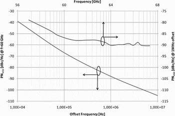
The tuning characteristic of the free-running VCO is characterized by connecting the fine- and coarse-tune inputs together. The oscillation frequency is measured at the output of the frequency divider. The tuning characteristic at different temperatures is depicted in Fig. 12. With a tuning voltage between 0.2 and 4 V, the VCO exhibits a large relative tuning bandwidth of 22%. From −5 to +85°C the output frequency varies by ±0.85 GHz. For a carrier frequency of 60 GHz, the phase noise of the VCO (Fig. 13) is −67 dBc/Hz at an offset frequency of 100 kHz and −88 dBc/Hz at 1 MHz offset. Due to a high tuning slope of up to 10 GHz/V, phase noise degrades toward lower frequencies and amounts to −79 dBc/Hz at 57 GHz. At an oscillator frequency of 67 GHz, it improves to −90 dBc/Hz.
VCO tuning characteristic at T = −5, 25, 55, and 85°C; V CC = 3.3 V, V t,fine = V t,coarse.

VCO phase noise at f = 60 GHz and 1 MHz offset, T = 25°C, V CC = 3.3 V.

B) Upconverter
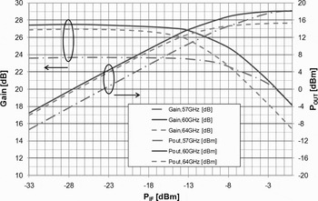
Figure 14 shows the measured upconversion gain and output power of the balanced upconverter versus input power at 57, 60, and 64 GHz. From 60 to 64 GHz, the overall upconversion gain is 26.4 dB, at 57 GHz it drops to 23.6 dB. The output referred 1 dB compression point is 14 dBm from 57 to 60 GHz and drops to 11.5 dBm at 64 GHz. The maximum saturated output power ranges from 15.5 to 18 dBm.
Measured output power P OUT and upconversion gain G C of the balanced upconverter versus input power at f IF = 50 MHz, V CC = 3.3 V, and T = 25°C.

The LO leakage at the RF output, caused by upconverter non-idealities and parasitic coupling effects is minimized using a static offset on the IF inputs of the upconversion mixers. Using this method, the LO leakage can be suppressed below −30 dBm by destructive superposition and the linear dynamic range of the upconverter can be increased by 20 dB. The quality of the upconversion is characterized in Single Sideband (SSB) mode. Between 57 and 64 GHz the image rejection is 24–32.5 dB as depicted in Fig. 15. The integrated power sensor provides a measure for the output voltage swing at the output of the PA and generates an almost linear output voltage from 1 mV to 1 V for output power levels between −20 to +15 dBm. It is used for LO leakage cancelation.
Measured image rejection of the balanced upconverter versus RF frequency (SSB operation mode, f IF = 50 MHz, P IF = −16 dBm, V CC = 3.3 V, T = 25°C).

C) Downconverter
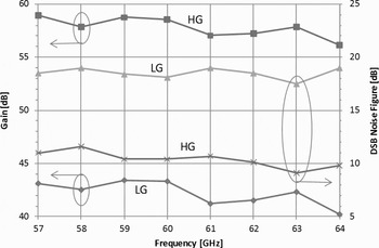
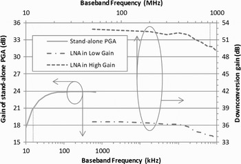
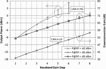
Figure 16 shows the downconversion gain and double-sideband noise figure versus RF input frequency for both LNA gain steps. The double-sideband noise figure ranges from 9 to 12 dB in high-gain mode and from 17.5 to 19 dB in low-gain mode. The high bandwidth of the LNA provides a gain flatness of 3 dB from 57 to 64 GHz. The 3 dB baseband bandwidth at 60 GHz RF input was found to be around 850 MHz to 1 GHz at 53 and 37 dB conversion gain, respectively (Fig. 17). The lower cut-off frequency of the baseband amplifier was verified on a stand-alone PGA test chip. As shown in Fig. 17, it was measured to be 16 kHz, which is much lower than the required 0.1% of the signal data rate [Reference Razavi13] and makes the receiver suitable for radar applications as well. As shown in Fig. 18, the maximum downconversion gain at 60 GHz RF input and 100 MHz IF output is 71 dB and the output referred 1 dB compression point was measured with −1 dBm. The input power at the chip-pads was −62 and −85 dBm, respectively. A PGA gain step resolution of 3 dB over a downconversion dynamic range of 35 dB ensures appropriate IF signal leveling to the ADC input.
Conversion gain and DSB noise figure for high-gain (HG) and low-gain (LG) modes of the LNA.

Downconversion gain versus baseband frequency at 60 GHz and lower cut-off frequency of the PGA.

Downconversion gain versus gain steps and maximum output power at 60 GHz RF input and 100 MHz IF output.

VI. CONCLUSIONS
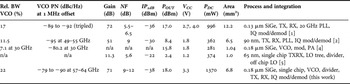
A highly integrated 60 GHz homodyne transceiver MMIC has been designed and fabricated using a SiGe:C HBT technology. A fundamental 60 GHz VCO covers the frequency range from 57 to 64 GHz with a large relative tuning bandwidth of 22%. An upconversion gain of 26.4 dB along with a high 1 dB output power compression of 14 and 18 dBm saturated output power have been achieved at 60 GHz. The downconverter exhibits a maximum gain of 71 dB and a noise figure of 9–12 dB from 57 to 64 GHz. On-chip AC coupling with a lower −3 dB cut-off frequency as low as 16 kHz eliminates DC-offsets prior to baseband amplification. The 3.25 × 2.1 mm2 MMIC consumes 1.37 W from the 3.3 V supply and requires few external components. A performance comparison with published 60 GHz transceivers/transmitters is given in Table 1.
Performance comparison for 60 GHz transceiver/transmitter chip-sets.

ACKNOWLEDGEMENTS
This work was part of the project EASY-A, which was funded by the German Federal Ministry of Education and Research (BMBF). The authors wish to acknowledge Mr. Z. Tong for providing the waveguide transition and all, who contributed to the layout, fabrication, assembly, and measurement of the chips.
 Hans Peter Forstner has been graduated as electrcial engineer in 1993 from the University of Applied Sciences Munich. As a principal engineer he is with Infineon Technologies AG since 1996. His background is GaAs- and SiGe RF circuit design, as well as SiGe mm-wave circuit design up to 80 GHz.
 Markus Ortner was born in 1977. He received his Dipl.-Ing. degree in mechatronics from the Johannes Kepler University of Linz, Austria, in 2005. In 2005, he joined Danube Integrated Circuit Engineering (DICE) in Linz, Austria, a majority-owned subsidiary of Infineon Technologies. There, he gained hands-on experience as an application engineer for radio frequency circuits. From 2008, he started working on millimeter-wave circuit design as Ph.D. student within Infineon.
 Ludger Verweyen (Dipl.-Ing./Ph.D.) graduated from RWTH Aachen in 1994/98. He has been working on a broad range of RF projects, designing GaAs based mmW-MMICs at Fraunhofer IAF in the 1990s, leading development projects on power amplifier and switch modules for wireless communication systems at TriQuint Semiconductor, and managing projects on RF products and mmWave-based transceivers based on Si technologies at Infineon Technologies in Munich.
 Herbert Knapp received the diploma and Ph.D. degrees in electrical engineering from the Technical University Vienna, Austria, in 1997 and 2000, respectively. In 1993 he joined Siemens, Corporate Technology, in Munich, Germany, where he worked on circuits for wireless communications and high-speed data transmission. He is now with Infineon Technologies, Munich, Germany, and is engaged in the design of circuits for automotive radar applications.