I. INTRODUCTION
Work on flexible thin-film transistors (TFTs) using amorphous In–Ga–Zn–O (a-IGZO) Reference Nomura, Ohta, Takagi, Kamiya, Hirano and Hosono1 has revitalized interest in oxide-based electronic devices owing to their high mobility, low temperature process, good transparency to visible light, and relatively larger area coating with more uniformity. Reference Nomura, Ohta, Takagi, Kamiya, Hirano and Hosono1–Reference Jeong7 This research area has risen to a significant advance driven by researchers since a decade, resulting in publications reporting TFTs based on ZnO, SnO2, InZnO (IZO), and In2O3. Reference Wager8–Reference Choi, Jeon, Kim, Shin, Kim and Chung25 ZnO TFTs have been studied more intensively because this structure is anticipated to exhibit better performance than a-Si: H and organic TFTs owing to the large Hall mobility (200 cm2 V−1 s−1) of single-crystal ZnO Reference Feng26 and the prepared formation of semiconducting crystalline thin films even on unheated substrates at room temperature. Nevertheless, the channels of ZnO TFTs are polycrystalline. Therefore, the uniformity in large areas is poor due to defects on grain boundaries, exhibiting high carrier concentrations even at room temperature due to native defects such as zinc interstitials and oxygen vacancies. Thus, it has been hard to control the threshold voltage shift and sustain against bias stress instability under various stress conditions such as thermal, light, and environmental. Reference Kamiya and Hosono2,Reference Jeong27
The most significant characteristic of the oxide semiconductor is the carrier concentration, which should be controllable over several orders of magnitude. However, oxides possess the high carrier concentration without unintentional post annealing. Reference Facchetti and Marks28 Oxide materials such as doped SnO2, In2O3, and ZnO have been used for various optoelectronic applications owing to their highly conducting and transparent properties. Reference King and Veal29–Reference Calnan and Tiwari31 For optoelectronics applications, the transparent conducting oxides are required high density of mobile electrons (typically >1018 cm−3) with high transparency. Reference Minami32 Nevertheless, amorphous oxide semiconductors (AOSs) channel layers are required typically carrier concentrations <1017 cm−3 for achieving good switching operation. Reference Grundmann, Frenzel, Lajn, Lorenz, Schein and von Wenckstern33
As discussed above, the pure form of oxide semiconductors is polycrystalline and possesses the high carrier concentrations. Reference Parthiban, Ramamurthi, Elangovan, Martins and Fortunato34 On the other hand, the same binary oxide compounds, mixing an appropriate amount form amorphous phases such as Zn–In–O (a-ZIO) and Zn–Sn–O (a-ZTO). Reference Hosono3,Reference Chiang, Wager, Hoffman, Jeong and Keszler11 In general, the mixing of two or more cations with different ionic charges and sizes is effective to enhance the formation of an amorphous phase, suppressing crystallization and carrier concentration. Reference Hosono3 Based on this AOSs are mixing multicomponent systems. Moreover, several AOSs have been invented such as a-In–Zn–O (a-IZO), Reference Hosono3 (a-IGZO), Reference Nomura, Ohta, Takagi, Kamiya, Hirano and Hosono1 a-Hf–In–Zn–O (a-HIZO), Reference Chong, Jo and Lee35,Reference Kim, Kim, Lee, Park, Kim, Park, Lee, Lee, Park and Kim36 a-ZTO, Reference Chiang, Wager, Hoffman, Jeong and Keszler11 a-Ga–Zn–Sn–O (a-GZTO), Reference Fortunato, Pereira, Barquinha, Botelho do Rego, Gonçalves, Vilà, Morante and Martins37 a-Al–Sn–In–Zn–O (a-ATIZO), Reference Cho, Yang, Byun, Ryu, Park, Hwang, Yoon and Chu38,Reference Yang, Cho, Ryu, Park, Hwang, Jang and Jeong39 a-Al–Zn–Sn–O (a-AZTO), Reference Cho, Yang, Byun, Shin, Ryu, Park, Hwang, Chung, Cheong and Yoon40 etc. The a-ZTO has identified as an excellent AOS for earth abandoned and low-cost applications. However, the TFT fabrication required a high temperature annealing at >200 °C which is not suitable for flexible substrates. Reference Yang, Huh, Oh, Lee, Kim, Oh, Jeong, Hwang and Kim41 In contrast, the indium-oxide-based AOSs have demonstrated on flexible substrates with an excellent performance. Reference Park, Kim, Stryakhilev, Lee, An, Pyo, Lee, Mo, Jin and Chung42–Reference Hsu, Chang and Cheng44
Many amorphous oxide active channel layers have been developed using metal cations as carrier suppressors to control carrier concentrations for TFT devices, achieving high mobility in the range of 10–20 cm2 V−1 s−1, which depends upon deposition and post-processing conditions. Even though ternary or multi-metal oxide TFTs have high mobility, they often suffer from severe bias, light and environmental instabilities, limiting their potential applications. Reference Jeong27 For instability, three degradation models have been proposed which can be considered as plausible mechanisms such as trapping of photogenerated hole carriers, the creation of ionized oxygen defects, and the photodesorption of oxygen related molecules. Reference Lee, Jung, Son, Park, Kim, Choi, Jeong, Kwon, Koo and Lee45–Reference Chowdhury, Migliorato and Jang49 The trapping of photogenerated hole carriers can be controlled by suitable dielectric and passivation layer. However, the creation of ionized oxygen defects and photodesorption of oxygen, to find out the solution for this, a high bonding strength between dopants and oxygen could be controlled to diffuse out oxygen and creation of oxygen defects. Reference Jeong27 The defects center can be an oxygen vacancy defect, metal interstitial, or hydrogen-related complex. Among the ranges of defects, the negative bias illumination stress instability is often attributed to oxygen vacancy defects. Reference Ji, Kim, Jung, Park, Choi, Kim, Hwang, Lee, Hwang and Jeong50,Reference Ryu, Noh, Choi and Chang51 The possibility of an oxygen vacancy defect is when a neutral oxygen vacancy defect accepts a hole carrier to form a positive oxygen vacancy defect where an oxygen vacancy acts as a donor-like trap. Reference Jeong27 The origin of vacancy defects creation in the active channel layer has been described in more detail in the review papers. Reference Jeong27 The beginner can understand bias stress instability and oxygen vacancy creation which have been explained in more detail in a review paper. Reference Jeong27,Reference Nathan, Lee, Jeon and Robertson52,Reference Kim, Jeon, Park, Kim, Son, Seon, Seo, Kim, Lee and Chung53 Moreover, the mechanisms of oxygen vacancy defect creation have been explained in more depth in the review paper with suitable explanations. Reference Jeong27,Reference Nathan, Lee, Jeon and Robertson52,Reference Kim, Jeon, Park, Kim, Son, Seon, Seo, Kim, Lee and Chung53
Nomura et al. first introduced gallium (Ga) into a-IZO, which has subsequently been shown to endorse amorphicity, controlling carrier concentration and oxygen vacancy via strong bonding strength because the bonding strength of Ga–O is stronger than In–O and Zn–O. Reference Nomura, Ohta, Takagi, Kamiya, Hirano and Hosono1 Subsequently, Hf and Zr are introduced instead of Ga into a-IZO TFTs, which have shown high stability under bias stress and environmental conditions Reference Chong, Jo and Lee35,Reference Park, Kim, Park, Mo, Kim and Jeong54 though the reported mobility is lower than that of the high performance a-IGZO TFTs. This work claimed the reason for improved stability that the bonding strength of Hf–O and Zr–O is stronger than that of In–O, Ga–O, and Zn–O which suppress the carrier concentrations creation via oxygen vacancy and enhance the stability of TFTs. Reference Chong, Jo and Lee35,Reference Park, Kim, Park, Mo, Kim and Jeong54 After, numerous other carrier suppressors or “oxygen getters” Reference Hennek, Smith, Yan, Kim, Zhao, Dravid, Facchetti and Marks55 have been investigated such as Ti, Reference Chong, Han, No and Kim56,Reference Aikawa, Nabatame and Tsukagoshi57 W, Reference Aikawa, Nabatame and Tsukagoshi57–Reference Aikawa, Darmawan, Yanagisawa, Nabatame, Abe and Tsukagoshi59 Gd, Reference Park, Kim, Kim and Lee60 Ba, Reference Kim, Gunduz, Yoon, Kim, Al-Ghamdi and Yakuphanoglu61–Reference Banger, Peterson, Mori, Yamashita, Leedham and Sirringhaus63 Sr, Reference Banger, Peterson, Mori, Yamashita, Leedham and Sirringhaus63,Reference Yoon, Kim, Jeong, Kim, Rim and Kim64 Si, Reference Aikawa, Nabatame and Tsukagoshi57,Reference Chong, Chun and Lee65,Reference Chong, Kim and Lee66 Sc, Reference Choi, Kim, Jeong, Bae, Kim, Hong and Yu67 Y, Reference Ting, Chang, Li and Wang68–Reference Shin, Kim, Jeong, Du Ahn and Kim70 La, Reference Park, Kim, Kim and Lee71 Ta, Reference Park, Kim, Park and Chung72,Reference Lan, Xiong, Xiao, Li, Xu, Yao, Wen and Peng73 Mg, Reference Kim, Jeong, Du Ahn, Shin, Kim, Kim, Ryu, Park, Seon and Lee74 Ce, Reference Koo, Kang, Kim and Hong75 Sn. Reference Jang, Raja, Kim, Lee, Kim and Yi76 To explain the role of a carrier suppressor, some studies have postulated that ionic size and metal–oxygen bonding strength are the key factors to control carrier concentrations. Reference Hennek, Smith, Yan, Kim, Zhao, Dravid, Facchetti and Marks55 But some studies have argued that lower electronegativity is desired, Reference Choi, Kim, Jeong, Bae, Kim, Hong and Yu67,Reference Park, Kim, Kim and Lee71 while some studies argued that higher values better control oxygen vacancies. Reference Park, Kim, Park, Mo, Kim and Jeong54 To improve the stability of oxide TFTs, strong oxygen binders have been identified as a key factor that lead to improved bias stress instability of TFTs. Reference Yang, Huh, Oh, Lee, Kim, Oh, Jeong, Hwang and Kim41,Reference Park, Kim, Park, Mo, Kim and Jeong54,Reference Aikawa, Nabatame and Tsukagoshi57 However, a clear method for choosing appropriate carrier suppressor dopants associated with their ionic size, electronegativity, and metal–oxygen bonding strength to enhance the mobility and stability of TFTs is yet to be reported. In this work, we discuss the role of dopants associated with high Lewis acid strength (L) and bonding strength of dopant and oxygen as carrier suppressors and strong binder in amorphous indium-oxide-based TFTs, presents a method for choosing effective carrier suppressor dopants to enhance the performance and stability of TFTs.
II. ROLE OF CARRIER SUPPRESSOR AND STRONG BINDER DOPANTS IN AMORPHOUS OXIDE TFTs
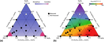
In this section, we discuss the role of the carrier suppressor and strong binder in AOS TFTs. To understand the role of the carrier suppressor, it is useful to compare systems undoped and doped carrier suppressor AOSs such as a-IZO and a-IGZO. As can be seen in Fig. 1(a), Reference Kamiya and Hosono2,Reference Nomura, Takagi, Kamiya, Ohta, Hirano and Hosono4 a-IZO has higher electron mobility than a-IGZO, but is significantly more difficult to control at the low electron concentrations which are required for TFTs (far below 1017 cm−3). The first-principles density-functional theory implies that In–O acts as a mobility enhancer in the a-IGZO system, Zn–O acts as a network former, and Ga–O acts as a carrier suppressor. Reference Kamiya, Nomura and Hosono5 Ga–O bonding strength is much stronger than In–O and Zn–O bonding strength, meaning that the incorporation of Ga suppresses the formation of oxygen deficiencies and the consequent generation of mobile electrons. On the other hand, the incorporation of high Ga content deteriorates the electron mobility [Fig. 1(b)]. Therefore, the addition of an appropriate amount of suppressor ions that form substitution doping and strong chemical bonds with oxygen ions is important for stable AOS materials and TFTs. The strong bonding strength between suppressor dopant and oxygen resulted that it diminishes an oxygen vacancy (V O) that suppress the carrier concentrations because one oxygen vacancy contributes two electrons in the conduction band. Incorporation of high Lewis acid strength and strong oxygen binder dopants could suppress the formation of shallow oxygen vacancy defects as well as deep oxygen vacancy defects in the active channel layers. Therefore, the addition of oxygen binders into the metal oxide channel layer should be chosen vital quantity to secure realistic transport properties, as well as the good photostability. Reference Yang, Huh, Oh, Lee, Kim, Oh, Jeong, Hwang and Kim41
(a) Amorphous formation and (b) electron transport properties of In2O3–Ga2O3–ZnO thin films. The values in (b) denote the electron Hall mobility (cm2 V−1 s−1) with density (1018 cm−3) in parentheses. Reproduced with permission from Ref. Reference Nomura, Takagi, Kamiya, Ohta, Hirano and Hosono4. Copyright 2006, Jpn. J. Appl. Phys.

The strong bonding strength between suppressor and oxygen enhances the stability of TFTs. From these arguments, we could understand that the carrier suppressor dopants and oxygen bonding are significantly important to enhance the performance and stability of TFTs. Most of the carrier suppressors have been chosen based on the electronegativity of metal dopants in the amorphous oxide matrix rather considering effective charge, ionic size, and metal–oxygen bonding strength. Reference Honglei, Mingyue and Qun58,Reference Kim, Kim, Rim, Jeong, Kim, Yoon and Kim62,Reference Chong, Chun and Lee65 Since Ga doped into a-IZO, subsequently, numerous other carrier suppressors have been investigated based on the electronegativity of metal ions. To explain the role of a carrier suppressor in a-IZO properties enhancement, some studies have postulated that metal ion electronegativity is the key factor of oxygen suppressor. Reference Park, Kim, Park, Mo, Kim and Jeong54,Reference Chong, Han, No and Kim56 In addition, ionic radius size is also important to choose an efficacy carrier suppressor. Reference Hennek, Smith, Yan, Kim, Zhao, Dravid, Facchetti and Marks55 The Ga has an ionic radius significantly smaller than that of In and similar to that of Zn, so that Ga placed as substitution sites act as a carrier suppressor in an amorphous oxide. Conversely, lanthanum (La) has larger ionic radii than those of In and Zn which may not be placed as substitution sites that lead to cause local structure disruption, hindering charge transport, degraded mobility, and stability of TFTs. Reference Park, Kim, Kim and Lee71 The zirconium (Zr), Reference Park, Kim, Park, Mo, Kim and Jeong54 hafnium (Hf), Reference Chong, Jo and Lee35 silicon (Si), Reference Aikawa, Nabatame and Tsukagoshi57,Reference Chong, Chun and Lee65,Reference Chong, Kim and Lee66 titanium (Ti), Reference Aikawa, Nabatame and Tsukagoshi57 tungsten (W), Reference Aikawa, Nabatame and Tsukagoshi57–Reference Aikawa, Darmawan, Yanagisawa, Nabatame, Abe and Tsukagoshi59 and tantalum (Ta) Reference Park, Kim, Park and Chung72,Reference Lan, Xiong, Xiao, Li, Xu, Yao, Wen and Peng73 doped indium-oxide-based TFTs have shown that the high bonding strength of dopants is one of the key factors to determine the stability. The W-, Si-, and Ti-doped indium oxide suggested higher bonding strength of dopants and oxygen is an efficacy to improve the performance and stability of TFTs. Reference Aikawa, Nabatame and Tsukagoshi57 However, La-doped a-IZO had reported lower mobility than that of high performance a-IGZO even though the bonding strength of La–O (∼799.0) is higher than that of Ga–O. Reference Kerr77 The reason for this low performance could be due to the ionic size of La which is larger than that of In and Zn. Reference Park, Kim, Kim and Lee71 Based on the above-mentioned postulates we propose that the smaller ionic size, high effective charge, high electronegativity, and strong metal-oxide bonding strength of dopants are the important key factors to determine the mobility and stability of TFTs.
III. RECENT PROGRESS OF CARRIER SUPPRESSOR AND STRONG BINDER DOPED INDIUM-OXIDE-BASED TFTs
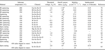
In this section, we have discussed the recent progress of carrier suppressor and strong binder doped amorphous indium-oxide-based TFTs from first reported a-IGZO TFTs to up to now and examined their properties, tabulated in Table I. In recent years, number of dopants incorporated instead of Ga into amorphous indium-oxide-based TFTs to find out an effective carrier suppressor and bonding strength enhancer. The obtained significant novel amorphous indium-oxide-based TFTs and their properties, merits, and demerits are briefly discussed to find out an effective carrier suppressor and strong binder.
TFT properties of various metal cation doped amorphous indium-oxide-based channel layer.

A. Ga–In–Zn–O
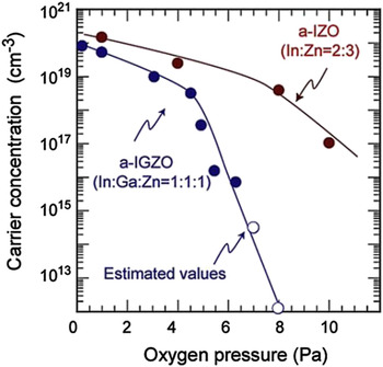
IZO is an excellent AOS. However, the carrier concentration is quite high, and this has impeded TFT device performance such as mobility and stability under thermal and light. To overcome this problem, in 2004, Ga introduced as a carrier suppressor in the IZO matrix and distantly reduced the carrier concentrations as shown in Fig. 2. Reference Nomura, Ohta, Takagi, Kamiya, Hirano and Hosono1,Reference Nomura, Takagi, Kamiya, Ohta, Hirano and Hosono4 The carrier concentration in the a-IGZO is significantly reduced to below 1013 cm−3 by reducing partial pressure oxygen from 0 to 8 Pa, whereas it remains at 1018 cm−3 in the a-InZnO deposited under the same conditions. Reference Nomura, Ohta, Takagi, Kamiya, Hirano and Hosono1,Reference Nomura, Takagi, Kamiya, Ohta, Hirano and Hosono4 The Ga is believed to attract oxygen ions tightly owing to its high ionic potential (+3 valence and small ionic radius), and thereby suppresses electron injection which is caused by oxygen ions escaping from the thin film since the vacancy of one oxygen contributes two electrons in the conduction band. The field effect mobility evaluated from the saturation region was ∼12 cm2 V−1 s−1, which is larger than that of a-Si: H TFT; however, the stability of a-IGZO TFTs still remains the most critical issue for bias thermal and light induced studies. Reference Jeong27
Controllability of a-IGZO and a-IZO films, relationship between carrier density and oxygen pressure during deposition. Reproduced with permission from Ref. Reference Nomura, Takagi, Kamiya, Ohta, Hirano and Hosono4. Copyright 2006, Jpn. J. Appl. Phys.

B. Hf–In–Zn–O
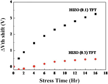
In 2009, Chang et al. introduced Hf as a carrier suppressor in the a-IZO matrix and improved the bias stress stability of the TFT, while the mobility comparable to a-IGZO TFTs. Reference Kim, Kim, Lee, Park, Kim, Park, Lee, Lee, Park and Kim36 TFTs with a-HIZO active channels exhibit good electrical properties with field effect mobility of around 10 cm2 V−1 s−1, subthreshold swing (ss) of 0.23 V/decade, and high I on/I off ratio of over 108. Figure 3 shows that, under a bias-temperature stress test, the HIZO TFTs with 0.3 mol% Hf content showed only a 0.46 V shift in threshold voltage, compared with a 3.25 V shift in HIZO TFT for 0.1 mol%. The Hf ions played a key role in improving the instability of TFTs due to high oxygen bonding ability.
The variation of V th for the HIZO (0.1) and (0.3) TFTs as a function of the bias thermal stress time. The following conditions of BTS were applied to both TFTs: a gate to source voltage (V GS) of 20 V, drain to source voltage (V DS) of 10 V, and substrate temperature of 60 °C. The TFTs were kept under the BTS condition for 16 h. Reproduced with permission from Ref. Reference Kim, Kim, Lee, Park, Kim, Park, Lee, Lee, Park and Kim36. Copyright 2010, American Institute of Physics.

C. Zr–In–Zn–O
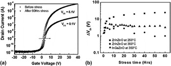
In 2009, J. S. Park et al. reported a novel InZrZnO TFT where the Zr had incorporated as a carrier and oxygen vacancy formation suppressor. Reference Park, Kim, Park, Mo, Kim and Jeong54 They postulated that Zr cations act as carrier suppressors. The electron carrier concentrations in the ZrInZnO films were found to decrease from 4 × 1016 cm−3 to 1 × 1014 cm−3 with increasing Zr concentrations. Figure 4(a) shows the transfer characteristics of the Zr0.4 In1.2Zn0.4O3 TFTs annealed at 350 °C for 2 h. The ZrInZnO TFTs exhibited a field-effect mobility of 3.9 cm2 V−1 s−1, a ss value of 0.98 V/decade, a V th of 1.6 V, and an I on/I off ratio of approximately 107. In addition, InZrZnO TFTs had been investigated and compared with IGZO TFTs under the bias stress of a drain-current stress of 3 mA at V DS = 10 V which was applied to the sample for a period of 60 h. The variation of V th for the ZrInZnO TFT device during the application of the on-state current stress is shown in Fig. 4(b). The stabilities of the a-IGZO TFT sample annealed at 350 °C and the ZrInZnO TFT samples annealed at 250 and 350 °C have been compared. The ZrInZnO device annealed at 250 °C showed a large positive shift (∼24 V) in V th after the application of the bias stress for 60 h. However, the ZrInZnO device annealed at 350 °C exhibited a dramatic improvement; specifically a 0.99 V shift in V th after the 60 h bias stress. Compared with InGaZnO TFTs, the better stability of the ZrInZnO TFT devices can be attributed to more suppression of the carrier concentration and stronger binding energy of the Zr in the ZrInZnO channel layer. These overall transfer characteristics are shown in Fig. 4(b). It has been shown that these ZrInZnO TFTs have excellent stabilities under long-term bias stresses.
(a) The transfer curve after 60 h bias stress. (b) The stability data comparison of a-InGaZnO and ZrInZnO TFTs. Reproduced with permission from Ref. Reference Park, Kim, Park, Mo, Kim and Jeong54. Copyright 2009, Wiley Publications.

D. Al–In–Zn–Sn–O
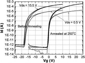
In 2009, Cho et al. invented a novel quaternary a-Al–Sn–In–Zn–O (ATIZO) channel layer and the transfer characteristics of ATIZO TFTs before and post-annealed conditions are shown in Fig. 5. Reference Cho, Yang, Byun, Ryu, Park, Hwang, Yoon and Chu38 The a-ATIZO used as a channel layer and high-K-Al2O x used as the gate insulator for fabrication of TFT at 250 °C. Reference Cho, Yang, Byun, Ryu, Park, Hwang, Yoon and Chu38 The ATIZO TFT exhibited a field effect mobility of 30.2 cm2 V−1 s−1, a ss of 0.17 V/dec, and an on/off current ratio of 109. Reference Yang, Cho, Ryu, Park, Hwang, Jang and Jeong39
Transfer characteristics of ATIZO TFTs with the active layer deposited at room temperature before and after annealing at 250 °C. Reproduced with permission from Ref. Reference Cho, Yang, Byun, Ryu, Park, Hwang, Yoon and Chu38. Copyright 2009, IEEE Electron Device Lett.

E. In–X–O
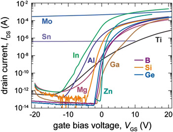
In 2009, Kumomi et al. explored indium-based ternary AOS, i.e., In–X–O with Mg, Al, Si, Ti, Zn, Ga, Ge, Mo, and Sn channel layer materials. Reference Kumomi, Yaginuma, Omura, Goyal, Sato, Watanabe, Shimada, Kaji, Takahashi and Ofuji14 The dopants which were chosen based on their ionic radii and electron affinities. Figure 6 shows the transfer curve of doped indium-oxide-based AOS TFTs. In this work, Si-, Ge-, and B-doped In–O TFTs achieved higher performance than other dopants. The Mo-, Ti-, and Sn-doped In–O TFTs are shown more conductive. The reason for conductive transfer characteristics of Mo-, Ti-, and Sn-doped indium oxide TFTs could be the excess Mo, Ti, and Sn doping amount and oxygen partial pressure.
Transfer characteristics of amorphous In–X–O TFTs at the optimum compositions. Reproduced with permission from Ref. Reference Kumomi, Yaginuma, Omura, Goyal, Sato, Watanabe, Shimada, Kaji, Takahashi and Ofuji14. Copyright 2010, American Institute of Physics.

F. Si–In–Zn–O
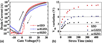
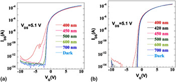
In 2010, Chong et al. reported a-Si–In–Zn–O TFT with a high field effect mobility of 21.6 cm2 V−1 s−1 and an I on/I off of 106 at a process temperature of 150 °C which is suitable for flexible display applications. Reference Chong, Chun and Lee65 The stability of a-SIZO TFT was compared with a-IZO and a-IGZO TFTs as shown in Fig. 7(a). Reference Chong, Chun and Lee65 The a-SIZO TFT showed a 3.7 V shift for threshold voltage (V th) compared with 10.8 V shift in IZO TFT after bias temperature stress. The performance of the a-SIZO TFT was compared with those of a-IZO and a-GIZO TFTs after a bias-thermal stress (BTS); drain current (I D) of 3 µA at drain-voltage of 10 V for 420 min to find the effect of Si on the stability of a-SIZO TFT as shown in Fig. 7(b). As the stress time increased, V th shifted positively for all TFTs. A large positive shift of V th, 10.8 V, was observed for IZO TFT after BTS. However, a positive shift of V th by only 3.7 V was realized for a-SIZO TFT even with only 1 wt% Si in the IZO system. This result indicates that the a-SIZO TFT is more stable than the a-IZO and a-GIZO TFTs. In the case of low processing temperature, including annealing treatment below 150 °C, all these characteristics showed enhanced mobility and bias thermal stability compared with those of others. The electrical properties of the SIZO TFTs confirmed that µFE decreased with increasing Si concentration, indicating that Si was acting as a carrier suppressor due to reducing V O in the SIZO system, due to higher bonding-strengths of silicon (775 kJ/mol) than those of zinc (385 kJ/mol) and indium (470 kJ/mol). Reference Chong, Kim and Lee66
(a) Comparison of transfer curves. (b) Bias-stress stability studies of post-annealed a-IZO TFT, a-GIZO TFT, and a-SIZO TFT with the same deposition condition using optimized post-annealing temperature. Reproduced with permission from Ref. Reference Chong, Chun and Lee65. Copyright 2010, American Institute of Physics.

The light illumination response of the (a) a-IZO-TFT and (b) a-TIZO-TFT (adapted from Ref. Reference Lan, Xiong, Xiao, Li, Xu, Yao, Wen and Peng73). Reproduced with permission from Ref. Reference Lan, Xiong, Xiao, Li, Xu, Yao, Wen and Peng73. Copyright 2013, American Institute of Physics.

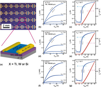
Transfer characteristics of post-deposition annealed a-IWO, TiIO, and SiIO TFTs. Reproduced with permission from Ref. Reference Aikawa, Nabatame and Tsukagoshi57. Copyright 2013, American Institute of Physics.

G. Ta–In–Zn–O
In 2013, Lan et al. developed a novel Ta-doped In–Zn–O (a-TIZO) TFTs which exhibit a field effect mobility of 11 cm2 V−1 s−1 with I on/I off of 109. Reference Lan, Xiong, Xiao, Li, Xu, Yao, Wen and Peng73 This study confirmed that Ta suppresses oxygen from out-diffusing during annealing, resulting in improving the bias stability under positive bias stress and light induced conditions. Furthermore, this work suggested that owing to its wider band gap and lower absorption of Ta2O5 the a-TIZO-TFT exhibited better stability under light illumination than a-IZO-TFT.
H. W, Ti, Si–In–O
In 2013, Aikawa et al. invented a novel tungsten-, titanium-, and silicon-doped amorphous indium oxide (WIO, TiIO, SiIO) TFTs at a process temperature of 150 °C. Reference Aikawa, Nabatame and Tsukagoshi57 50 The WIO, TiIO, and SiIO TFTs have reported a saturation field effect mobility of ∼30, 32, and 17 cm2 V−1 s−1 with an I on/I off ratio of 109. Reference Aikawa, Nabatame and Tsukagoshi57 This work proposed a new mechanism that the presence of a tiny amount of dopants prevents crystallization and leads to the formation of a very flat and smooth surface that reduces the degradation of carrier mobility. Another important key point reported that the higher bonding-dissociation energy, which means higher bonding strength between dopants and oxygen, became less sensitive when thermal annealing. If the energy of the metal-to-oxygen bond is low, then oxygen can be easily released during thermal annealing and bias stress, which increases the carrier density. In contrast, if a dopant with high bond-dissociation energy (to the oxygen atom) resulted it is difficult to create oxygen vacancy. Based on the bonding strength concepts, they suggested that high bonding strength of Si–O-doped metal oxide be efficacy to improve the stability and mobility of TFTs. However, the proposed mechanism is in contrast with La-doped IZO TFTs because La–O (799.0) has high bonding strength which is similar to Si–O (799.6) bonding strength. The La-doped IZO TFTs reported lower mobility than the a-IZO and a-IGZO TFTs. Reference Park, Kim, Kim and Lee71,Reference Kerr77
I. Ga-, Yr-, Sc-, Ga-doped IZO
In 2013, Hennek et al. Reference Hennek, Smith, Yan, Kim, Zhao, Dravid, Facchetti and Marks55 studied chemical similarities and differences in ionic radius cations such as Ga3+, Sc3+, Y3+, and La3+ doped a-IZO TFTs. These ions doped with a-IZO channel layer and processed under identical conditions to understand how their dopant affects in a-IZO TFTs. These works concluded that the metal oxide lattice formation enthalpy and metal ionic radius are the best predictors of doped IZO oxygen getter efficacy. This work studied positive bias stress stability of Ga3+, La3+, Y3+, Sc3+ doped a-IZO TFTs. The bias stress stability has not improved even though the bonding strength of La–O, Y–O, and Sc–O is higher than Ga–O because of larger ionic size than Ga3+ that degraded the transport properties. This study indicates that ionic size and metal–oxygen bonding strength are the most important key parameters to improve the mobility and stability of metal oxide TFTs.
J. Sr, Ba-doped IZO
In 2013, Banger et al. reported high performance of Sr- and Ba-doped a-IZO TFTs after hydrolysis and post-annealed. Reference Banger, Peterson, Mori, Yamashita, Leedham and Sirringhaus63 The Sr- and Ba-doped semiconductors exhibit enhanced electrical stability and reduced threshold voltage shift compared with IGZO. The enhanced stability can be explained based on the higher Gibbs energy of oxidation of Ba and Sr compared with Ga. Ba and Sr metals were chosen as appropriate candidates to dope IZO based on the calculation of the Gibbs energy of oxidation and their larger cation radii. The Sr, and Ba replacement of Ga for the tighter oxygen binding alkaline earth metals is supposed to suppress, the formation of excess charge carriers in the oxide film, which may hinder charge transport and hence reduce device mobility. However, the larger cation radii dopants Ba and Sr contradict with La- and Y-doped IZO TFTs which suggested that larger ionic radii are not suitable for improved performance of TFTs. Reference Hennek, Smith, Yan, Kim, Zhao, Dravid, Facchetti and Marks55 The insertion of large atomic radius dopants makes it difficult for the Zn and In to be in their correct positions. Therefore, the large atomic radius of dopants could cause the creation of trap states. Reference Park, Kim, Kim and Lee71 Lattice distortion due to the large atomic radius of dopants results in the creation of defects, which could be one of the reasons for the reduction in µ. The strong bonding strength of Sr–O and Ba–O could be one of the reasons for enhanced stability of Ba- and Sr-doped a-IZO TFTs. Reference Kerr77 Since the bonding strength of Sr–O and Ba–O is greater than Ga–O which is one of the key factors to improve the stability via tightening oxygen bonding to suppress the formation of excess carrier concentrations in the active channel layer.
IV. HOW TO CHOOSE THE APPROPRIATE CARRIER SUPPRESSOR DOPANTS TO CONTROL CARRIER CONCENTRATIONS IN AMORPHOUS OXIDE TFTs
Most of the amorphous oxide TFTs have been developed based on the electronegativity and standard electrode potential of dopants. Reference Honglei, Mingyue and Qun58,Reference Kim, Kim, Rim, Jeong, Kim, Yoon and Kim62,Reference Chong, Chun and Lee65 Three decades ago, Wen et al., Reference Campet, Han, Wen, Manaud, Portier, Xu and Salardenne80 recently Kim research group Reference Kang, Lim, Lee, Kim and Kim81–Reference Kang, Lim, Na and Kim92 and Parthiban et al. Reference Parthiban, Ramamurthi, Elangovan, Martins and Fortunato34,Reference Parthiban, Elangovan, Ramamurthi, Martins and Fortunato93,Reference Parthiban, Gokulakrishnan, Elangovan, Goncalves, Ramamurthi, Fortunato and Martins94 have developed high-mobility Zr-, Germanium (Ge-), Sn-, W-, Nb-, Mo-, Si-, and Ti-doped indium oxide transparent conducting thin-films, which were followed by the development of empirical relations and postulates by Zhang. Reference Zhang95 The empirical relationship associated with electron negativity, ionic radii, and effective charge of dopants, was proposed by Zhang and defined the function as a scale for strength of Lewis acids. Lewis acid or base is defined as a pair of electron acceptor or donator, respectively. Strength defines how easily it is done by particular acid/base. A stronger Lewis acid will easily accept more electrons than a weaker one. Lewis acid–base interactions play an important role in understanding chemical bonds, relations, and equilibria. A scale for the Lewis acid strengths has been calculated from the dual parameter equation, one parameter is Z/r 2, where Z is the charge number of the atomic core and r is the ionic radius related to the electrostatic force, and another parameter is the electronegativity (χZ) of elements in valence states. The quantity of Z/r 2 was calculated with the use of ionic radii mainly from Shannon Reference Shannon96 and Dean. Reference Dean97 The equation for classification is derived from plotting Z/r 2 against χZ.
 $$L = {{Z \mathord{\left/ {\vphantom {Z r}} \right. \kern-\nulldelimiterspace} r}^2} - 7.7{\chi _{\rm{{\rm Z}}}} + 8.0\quad ,$$
where L is Lewis acid strength of element.
When choosing appropriate dopants, the following must be taken into account.
-
(1) The ideal doping cations should have smaller ionic radius (r k) which is associated with a higher effective nuclear charge (Z).
-
(2) According to the study of Wen et al., the high Lewis acid dopants polarize the electronic charge away from the oxygen 2p valence band more strongly than the weaker Lewis acids, this results in screening of the charge and weakens its activity as a scattering center hence increasing the mobility. The scattering center is one of the significant parameters deciding mobility if the scattering center is low that may expect high mobility. The high Lewis acid strength of elements suppresses scattering by oxygen interstitials that resulted in high mobility.
-
(3) The size of the ionic dopant should be smaller than that of the host materials; otherwise, the dopants will act as a defect which causes deterioration in the electrical properties. Reference Seo, Jeon, Hwang, Park, Ryu, Park and Bae79
-
(4) Choosing an appropriate amount of carrier suppressor dopants is more important to control carrier scattering; otherwise, excess dopants which act as ionized scattering centers lead to deteriorating mobility.
-
(5) The metal-oxide bonding strength of carrier suppressor dopant and oxide should be higher than the host metal oxide to control the carrier generation via formation of oxygen vacancy to enhance the stability of TFTs.
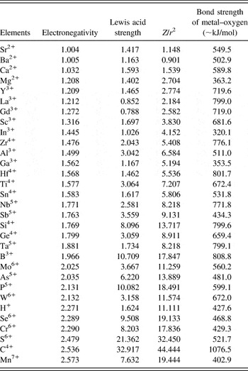
Based on the L, χz, and Z/r 2 and bonding strength of dopant and oxygen of the elements are tabulated in Table II. The L of the elements had a stronger influence on the effective charge and ionic radii than the electronegativity of the elements. As shown in Table II, the electronegativity of Ti4+, Zr4+, Ga3+, Hf4+, Al3+ is ∼1.5, Sb and Si is ∼1.7, B3+, Mo6+, and W6+ is ∼2.0, C and Mn7+ is ∼2.5. Even though the electronegativity is almost comparable, however, their L value is differing more because of Z/r 2. From Table II, it can be observed that the electronegativity of the dopant element is not only considered when designing novel metal oxide TFTs via suppression of the carrier concentrations. Another important parameter is bonding strength of metal and oxygen (M–O). If bonding strength is high it is expected to be more stable; therefore, it is necessary to compare bonding strength with their L of elements. The value of L and their M–O are tabulated in Table II. The bonding strength of metal and oxygen (M–O) such as La–O (799.0), Si–O (799.6), Ta–O (799.1), Zr–O (776.0), and Hf–O (801.7) Reference Kerr77 are almost the same. However, except La–O, others have been identified as efficacy dopants to suppress carrier concentration and improve stability, because the La has larger ionic size, smaller electronegativity, lower Z/r 2, and Lewis acid strength than indium and zinc that leads to low performance than other dopants. From these, we conclude that the strength of metal and oxygen is not only considered for when selecting appropriate dopants but also when selecting appropriate dopants for L relation to ionic radii and the effective charge of elements and metal-oxide bonding strength.
Lewis acid strength of elements and their metal-oxide bonding strength. Reference Kerr77

V. CONCLUSIONS
Since the first demonstration of TFTs using a-IGZO as a channel layer, there has been a rapid growth in oxide channel layer materials in recent years toward commercialization. Although the device performance of a-IGZO TFTs has been substantially improved, the device reliability in the presence of external light and gate bias stress remains a critical issue. At present, Samsung Electronics, Toppan, Sharp, and LG Display have demonstrated prototypes of active matrix liquid crystal display and active matrix organic light emitting diode panels that integrate a-IGZO TFT backplanes. In recent years, to overcome stability issues, Si, Hf, Zr, Ta, etc. have been incorporated instead of Ga as carrier suppressors into the IZO system which has successfully improved reliability.
From this review, we suggested that the L, Z/r 2, and M–O are the important key parameters to improve the stability and high performance of TFTs. Based on L, Z/r 2, and M–O, it is suggested that Ti4+, W6+, Ge4+, Ta5+, Nb5+, Si4+, B3+, and C4+ doped AOSs would be suitable for high performance and stability of TFTs. It is observed that the high L and bonding strength of the dopant act as a carrier suppressor for oxygen in the amorphous oxide system, and could, therefore, be effective for high performance TFT fabrication. Specifically, high L with high Z/r 2 and bonding strength of carrier suppressor and bonding strength enhancer dopants such as Ti4+, W6+, Ge4+, Si4+, B3+, and C4+, doping an appropriate amount in the amorphous oxide is predicted to be an effective carrier suppressor and strong binder in IZO to enhance the performance and stability and alternative to most studied a-IGZO TFTs. Adding high L with Z/r 2 and bonding strength of dopants as carrier suppressors in metal oxide TFTs but also suppress the carrier concentrations and enhance strong metal-oxide bonding strength, it also enhances the amorphous nature and lowers the temperature for processing. Additionally, high Lewis acid strength dopants results in screening of the charge and weakens its activity as a scattering center, therefore, increasing the mobility. In the case if the scattering center is low that may expect high mobility. The incorporation of a high L with high Z/r 2 and bonding strength dopant as a carrier suppressor into AOS-based TFTs is a useful route to produce improved stability and higher performance TFTs, which may enable the realization of next-generation flat panel displays. The proposed mechanism could be useful in the development of high stability and high performance next generation novel AOS TFTs.
ACKNOWLEDGMENTS
This research was supported by the MSIP (Ministry of Science, ICT, and Future Planning), Korea, under the “IT Consilience Creative Program” (NIPA-2014-H0201-14-1001) supervised by the NIPA (National IT Industry Promotion Agency).