Introduction
It is more than 22 years since the highest induced non-linearity within a silica (SiO2) optical fiber has been reported—5.8 pm/V when poling with 193 nm ArF exciplex emission in late 1994.[
Reference Fujiwara, Wong, Zhao, Fleming, Poole and Sceats
1
] Ultraviolet (UV) poling had achieved an order of magnitude over anything else reported in Refs. Reference Myers, Long and Brueck2–Reference Dontsova, Kablukov, Lobach, Dostovalov, Babin, Gladyshev, Dianov, Corbary, Ibsen and Kazansky7, and references therein. It was groundbreaking if correct, introducing practical non-linearity onto silicon (Si)-based platforms potentially making LiNbO3 obsolete overnight. Unfortunately, at first glance, the result appeared to defy the laws of physics in a material with no inversion symmetry. The failure to reproduce such results effectively consigned the work to the dustbin. Given the significance of those results, both at the time and in the future if it can be reproduced, this work provides an important commentary on a plausible mechanism that suggests a potential optoelectronic platform: water.
To unravel the mystery requires a brief review of how symmetry in these materials can be broken. The instantaneous and parametric non-linear optical phenomena induced within an optical fiber can, in the case where applied optical fields are not too large, be artificially described by a Taylor series expansion of the dielectric polarization density P(t) at time t in terms of the applied electrical field E(t):
where χ represents linear and higher order non-linear susceptibilities. The key photonic platform materials of Si, SiO2, and most silicate materials are centrosymmetric (no asymmetry in the overall electric field distribution giving rise to sufficiently large polarizability that can be easily manipulated through electronic field displacement with voltage). For example, the second-order term in Cartesian space,
 $P_i\left( t \right) = 2\sum\nolimits_{\,j,k} {d_{i,j,k}E_j\left( t \right)E_k(t),} $
where d is the non-linear tensor, associated with the Pockel's effect predicts a quadratic dependence on an applied electric field for distorting the polarizability that results in a linear index change. For the interrogating frequency, w, the expression for the polarizability with an applied field, E
app, has been reduced to[
Reference Fleming and An
5
]
From this behavior, a dependence on directly applied voltage is obtained. Non-centrosymmetric materials such as LiNbO3 (r coefficients between 8 and 30 pm/V) make use of this and subsequent effects that can be generated. The material mismatch between LiNbO3 and SiO2-based photonics has helped to limit widespread deployment of photonic circuits.
There are several ways of breaking symmetry in the tensor components describing polarizability. In recently reported Si devices, symmetry breaking by directly applying strain appeared to produce sizeable non-linear coefficients.[
Reference Jacobsen, Andersen, Borel, Fage-Pedersen, Frandsen, Hansen, Kristensen, Lavrinenko, Moulin, Ou, Peucheret, Zsigri and Bjarklev
8
] This was highly controversial given the strong centrosymmetric structure, the absence of any initial molecular dipole amenable to reorientation, and the resistance to mechanical deformation of the Si structure. Recently, however, the results have been explained as arising from strain-induced symmetry breaking of the SiN layers rather than the Si itself.[
Reference Khurgin, Stievater, Pruessner and Rabinovich
9
] The work, therefore, demonstrates the usefulness of direct optical field overlap to obtain practical device responses. SiN layers already have a defined local microscopic dipole that, particularly in interfacial film form, lends itself to deformation and alignment when significant strains are applied. The strain field has an equivalent effect to an electric field and is generally a combination of piezoelectric (negligible piezo coefficient for centrosymmetric materials) and flexo-electric contributions, the latter being of interest in understanding strain effects. The flexo-electric effect is well known in liquid crystals and more recently in solid crystals, polymers,[
Reference Singer, Kuzyk, Holland, Sohn, Lalama, Comizzoli, Katz and Schilling
10
] ceramics[
Reference Ma and Cross
11
,
Reference Yamaoka, Takahashi, Yamazaki, Terakado, Miyazaki and Fujiwara
12
] including perovskites. This is because in all these materials, the existing molecular dipole is already strong but randomized, so there is no pre-existing macroscopic polarization. By applying strain, randomization is removed and a macroscopic polarizability is induced giving rise to the observed strain gradient-induced net electro-optic (e.o.) effects.
Similarly, there is a dipole arising from Si–O bonds in SiO2 glass; however, the much more rigid constraint in tetrahedral geometry prevents similar strain-induced changes in the polarizability (in contrast to the flexibility of its longer range network). Poling, usually thermal or optical, is the method used to attempt to presumably break this tetrahedral centrosymmetry in optical fibers. It takes place in the high purity SiO2 cladding, so its rigid network geometry combined with amorphous distribution makes it difficult to break the inversion symmetry. A plausible argument is that poling has led to electro-restrictive like effects, through the attraction between the two electrodes, that have deformed the random nature of the glass through linear strains and possibly circumferential strains at the interface of the large air holes containing the attractive conductors to which large voltage is applied. Given the range of experiments looking to explore electro-restrictive effects, it is striking that this has not demonstrably generated coefficients on a scale approaching the result of Fujiwara et al.[
Reference Fujiwara, Wong, Zhao, Fleming, Poole and Sceats
1
] Electrostriction did account for third-order non-linearities induced by conventional poling.[
Reference Godbout, Lacroix, Quiquempois, Martinelli and Bernage
13
]
A simpler approach to symmetry breaking in the material is forcing charge movement and separation through impurities or defect sites in the glass into layers orthogonal to the propagation of light. This has been the most plausible model so far utilized in the study of poled optical fiber (and another system) non-linearities. It appears to account for the bulk of conventional poling results, potentially up to ~1 pm/V, though typically closer to 0.2 pm/V.[
Reference Fleming and An
5
,
Reference Kazansky, Dong and Russell
14
] It was insufficient to explain the anomalously high results of 1994, which exceeded six times this value.
Charge separation under an additional field during poling requires impurities. Some of these such as Na+ and OH− ions, which migrate toward the cathode and anode, respectively, arise in trace amounts within the lower quality outer SiO2 glass used in optical preform fabrication; nonetheless, despite methods of introducing more impurities, the quantities and internal fields that build up appear to limit the plausibility of explaining values even approaching 1 pm/V. Etching experiments did confirm the presence of OH− and marked depletion layers are left behind as Na ions are visibly transported away toward the cathode.[
Reference Fleming and An
5
] It has been interesting to observe that reproducibility at 1 pm/V was not always guaranteed. A partial explanation may be the optimal process for maximizing the induced field when the positive charges migrate over the fiber core.[
Reference Fleming and An
5
]
Understanding poling
So far, there has been no convincing explanation to account for the Fujiwara et al.’s results. Despite irreproducibility, the original authors remain adamant that the observed effects were real and that the experiments conducted with considerable care. Certainly, the 193 nm ArF laser was specifically set up to explore a range of light-matter interactions,[
Reference Canning, Sceats, Inglis and Hill
15
] including the Fujiwara et al.’s work. There was no evidence to suggest that the methods were inadequate fueling the mystery around the results. Still over time, these results were dismissed while poling of optical fibers remains a topical theme. For example, recent results demonstrate how even a weak effect compensated by long waveguide interaction lengths can be used to generate entangled photons with entangled polarization states for quantum applications.[
Reference Zhu, Tang, Qian, Helt, Liscidini, Sipe, Corbari, Canagasabey, Ibsen and Kazansky
16
] The possibility that such demonstrations could be achieved with shorter, robust, and practical lengths, even in low-loss silicate-based integrated optics, spurs the motivation for solving the Fujiwara et al.’s case.
Based on observations at the time the author proposes an alternative explanation, one that points to new directions and potentially new opportunities in non-linear switching; indeed a new field. Key points any model using SiO2 poled fibers as the benchmark has to consider include:
-
(1) Poling temperatures of a few hundred degrees remains way too low for any symmetry breaking in SiO2;
-
(2) Poling lifetimes are inconsistent with any solid phase symmetry breaking;
-
(3) There has been a correlation with OH− and poling magnitude,[
Reference Fleming and An
5
] the basis of charge separation models;
-
(4) The closer the core is placed to the anode channel, the higher the value of the induced coefficients suggesting surface or near-surface origins;
-
(5) The Fujiwara et al.’s results in a twin-hole fiber with a separation of only ~2 µm between channel and core, demonstrated a λ
Bragg shift to longer wavelengths with increasing V during poling AND an increase in grating reflectivity ΔR ~10 dB.[
Reference Fujiwara, Wong, Zhao, Fleming, Poole and Sceats
1
,
Reference Fleming and An
5
]
The remoteness of the depletion and channel layer from the guiding core, ~2 µm in the Fujiwara et al.’s work,[
Reference Fujiwara, Wong, Zhao, Fleming, Poole and Sceats
1
] would necessitate large values given the low percentage overlap of the optical field in this region (~1%—exact data is not available); this can be minimized with appropriate fiber design and core placement but to date this has not been reproduced. On the other hand, there is one overlooked possibility related to OH− diffusion—water in the air channels supporting the electrodes. This water can be introduced both during and after the fiber is fabricated. The literature has assumed all charge separation processes are driven within the fiber cladding, which appears generally true as evidenced by changes near the hole capillary channel supporting the electrode.
Here the author proposes that a water layer on the channel surfaces could help explain the anomalous result of 1994. The basis is that the optical fibers used by Fujiwara et al. were produced on a custom-made, relatively simple open-air draw tower. The presence of humidity and condensed moisture within the optical fiber channels and on the electrodes after drawing was guaranteed[
17
]—in contrast, typical fiber fabrication drawing would be undertaken within an enclosed tower containing an inert atmosphere such as Ar gas to ensure no moisture forms on or in the fiber. Importantly, unlike water in bulk, poled water at interfaces “no longer has the water dipoles randomly oriented” and therefore the e.o. coefficients of water are no longer necessarily negligible. Results reported in the literature for the e.o. coefficients of water provide additional support for this; examining this literature leads to the proposition that, with poling, there is a formation of an electrical double layer and a possibly self-assembled, charge-driven two-dimensional (2D) water structure on the surface of the channels that is largely responsible for the symmetry breaking and charge separation in the water. This will give rise to an enormous Pockels effect “in the soft water itself,” potentially large enough to explain the results measured at the core of the fiber. In addition, this effect can enhance conventional charge separation and field-build up itself.
The electrical double layer or equivalent
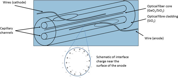
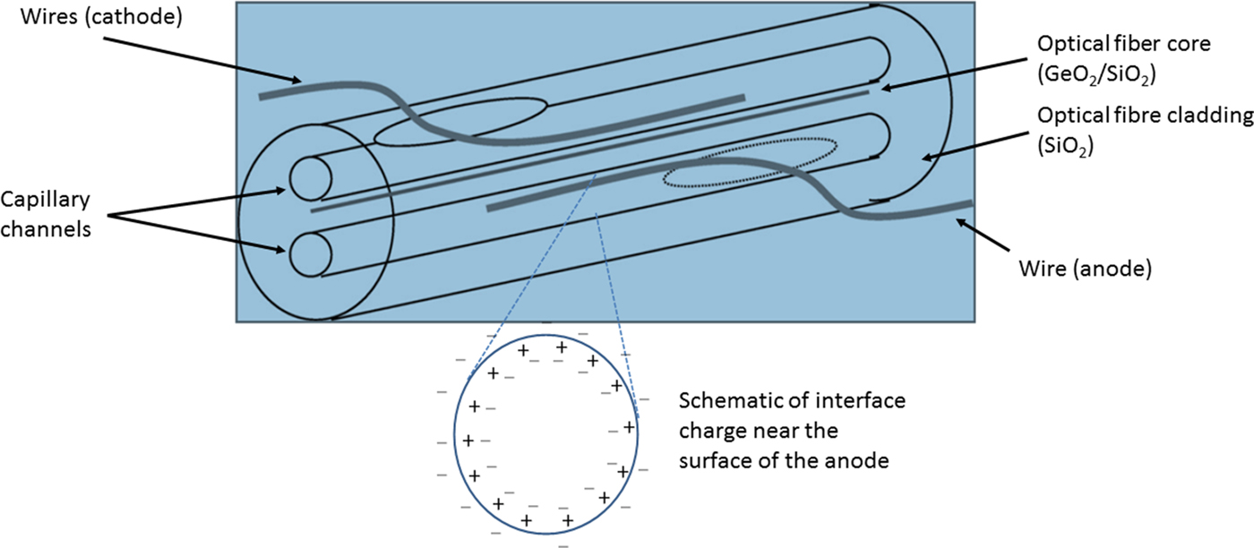
Figure 1 shows the schematic of the fabricated device used by Fujiwara et al. and illustrated by Fleming and An,[
Reference Khurgin, Stievater, Pruessner and Rabinovich
9
] copied and edited here to highlight where a water double layer would occur. An electrical double layer is a charged layer that appears at a surface when in contact with a fluid such as water. Ordinarily what triggers the formation of charges into layers at interfaces is the pre-existence or adsorption of charge on the solid interface, in this case, SiO2. Primarily through the dissociation of terminal silanol groups on the SiO2 surface, the SiO2 acquires a negative charge. This negative charge then leads to enhanced charge separation in water into layers of alternating charges that make up the double layer. Indeed, it is well known by forcing water flow through SiO2 channels, a voltage and current can be generated, the basis of electrophoresis diagnostic methods.[
Reference Takagi, Ohshima and Furusawa
18
] Recent works have used this as a potential novel source of power[
Reference Yung, Lu, Kostiuk and Kwok
19
,
Reference Canning, Buckley and Lyytikainen
20
] with sufficient voltage generated, and scalable with the number of channels,[
Reference Canning, Buckley, Huntington and Lyytikäinen
21
] a method for potential energy harvesting in microfluidic or millifluidic devices. This phenomenon is present when water is present.
Figure 1.
Close-up of the channel area after poling when water is present as a double layer on the surface of the glass. Hydrophilic attraction holds the layer well after bulk water affected by thermal agitation has evaporated. Adapted with permission from Ref. Reference Fleming and An5 (Ceramic Society of Japan, 1994).
The double layer in the water forms at a surface with an applied field—simply, water is a dipole self-ionizing to form an equilibrium with hydronium and hydroxyl ions:
The local molecular structure remains enigmatic because both surface confinement and removal of charge lead to orientation and close packing of water. For condensed water in the optical fiber, pure water on SiO2 is the primary contributor to the double layer with the proviso that this double layer potential is altered through the release of charges from the glass or electrode. A strong negative charged layer can build up further attracting impurities such as Na+ as well as injecting protons into the glass. Considerable scope for optimizing these effects exist.
In addition to charge separation, the density of water increases because of soft-matter dipole alignment and packing, potentially leading to molecular self-assembly expected in such confined water states. These are aligned dipoles that create charged crystal-like layers thought to possibly be similar to those reported in.[
Reference Forster, Ravel, Hodgson, Carrasco and Michaelides
22
] The interactions between them at the surface are strong enough to resist thermal motion of the water for a few layers. Regardless of the exact structural details, the net inversion symmetry of the water system is broken and all the usual rules assumed for bulk water no longer hold—in the liquid state the lack of thermal motion leads to an analogous viscous crystal-like film. Ordinarily, thermal motion prevents self-packing of the water molecules into lowest energy states and the water is random with no obvious asymmetry. But at an interface, without bonding self-packing, or self-assembly, of the molecular dipoles, can occur since the interface removes the degrees of freedom for thermal motion as well as absorbing some of the local energy. The migration of proton charges away leaves a dense negative index layer. Indeed, water at an interface is consistently measured to have a higher index than that of bulk water, n~(1.34–1.39) with large anisotropy[
17
] with scope to potentially exceed glass. In the case of water on indium–tin oxide electrodes, very large negative anisotropy between orthogonal and parallel indices (n
o−n
e = −0.2) has been reported.[
Reference Takagi, Ohshima and Furusawa
18
] This damping of thermal motion is sufficient for charge double layers to form, the thickness of which will depend on the applied fields and the quality of the surface layer. The fact that Fujiwara et al.’s result was observed with laser poling rather than thermal poling is consistent with a relatively cold, electromagnetic field process. By contrast, at the temperatures employed by thermal poling, including irradiation-induced energies, this is not true for SiO2.
Gigantic Pockels effect
Considering the layer in isolation, what is the potentially induced linear e.o. condition in this water double layer? Nanolayers on a surface are challenging systems to measure not the least of which is that its dimensions vary depending on temperature, poling voltage, and surface smoothness. The presence of such a layer with high indices may help draw an optical field if those indices can exceed SiO2.[
Reference Canning, Padden, Boskovic, Naqshbandi, de Bruyn and Crossley
23
] Fortunately, the surface of an optical fiber channel will almost certainly be the smoothest possible any amorphous network can have by virtue of its production method.[
Reference Canning, Andreone, Cusano, Cutolo and Galdi
24
] This should maximize properties including coefficients. Despite being difficult to measure given the sort range order <2 nm, there are several reports in the literature of the induced Pockels coefficient of interfacial water on electrode surfaces being very large. On rough electrodes, it has been measured as 60 up to 250 pm/V in r
13 and r
33 coefficients,[
Reference Nosaka, Hirabayashi, Kobayashi and Tokunaga
25
,
Reference Kanemaru, Nosaka, Hirako, Ohkawa, Kobayashi and Tokunaga
26
] exceeding LiNBO3. The same group had reported earlier on transparent indium–tin oxide electrodes measurements ranging over 500–1700 pm/V[
Reference Tokunaga, Nosaka, Hirabayashi and Kobayashi
27
] and smaller values on metallic GaN[
Reference Kanemaru, Nosaka, Hirako, Ohkawa, Kobayashi and Tokunaga
28
] consistent with oxide surfaces producing larger values—consequently, the double layer on SiO2 would be expected to be at the higher end. Demonstrating that this is a predominantly water interface effect, the air–water interface itself has an even larger measurable Pockels effect, up to 1.54 × 10⁵ pm/V.[
Reference Suzuki, Osawa, Yukita, Kobayashi and Tokunaga
29
] While the solid–water interfaces are attributed to both orientation of the dipoles and compression, this magnitude requires substantive orientation and structure changes at the water–air interface, consistent only with substantial movement of hydrogen away from the interface and restructuring of the water. Theoretical simulation of a 2D extended structure supports this argument[
Reference Pezzotti, Galimberti and Gaigeot
30
]—one would argue that this molecular rearrangement is a primary origin of surface tension in water drops. Nevertheless, while the physical details remain a subject of ongoing research, the sheer plausibility of inducing such large values using a soft material alters the potential of water and other dielectric liquids for optoelectronics, the basis of a new platform.
After poling, the double layer in[
Reference Nosaka, Hirabayashi, Kobayashi and Tokunaga
25
,
Reference Tokunaga, Nosaka, Hirabayashi and Kobayashi
27
] was estimated to be ~2 nm thick with a corresponding index change >7% (n > 1.39) from that of bulk water, larger than aligned water alone—this was negative for a positive bias. This magnitude is significant and both it and the thickness of the layer depend on the poling conditions applied—the likelihood that the surface roughness is larger than 2 nm in places suggests the film is less than optimal. Despite likely being an overwhelming underestimate, even with these parameters alone if the overlap integral approaches 1%, then significant changes are possible for ~1000 pm/V. Both the value of the coefficient and the local refractive index could be much higher with a thicker, more tightly bound film on the smoothest of SiO2 surfaces. Alternatively, the intense periodic 193 nm electromagnetic field used by Fujiwara et al. to write Bragg gratings can potentially periodically pole the water, similar to that used elsewhere[
Reference Dontsova, Kablukov, Lobach, Dostovalov, Babin, Gladyshev, Dianov, Corbary, Ibsen and Kazansky
7
]—the observed increased grating strength with applied voltage supports a periodic surface variation leading to periodic variations in interfacial water properties. Add to this the one-sided nature of the grating produced by high-intensity 193 nm grating writing[
Reference Janos, Canning and Sceats
31
] may also help to draw out the optical field toward the channel surface. However, it is also noted that an off-center grating experiencing any mechanical effect will also produce a shift in Bragg wavelength—in the case of Fujiwara et al. the shift to longer wavelengths would imply tensile bending. The contra-argument is that tensile bending should lead to reduced grating strength rather than increased as was observed.[
Reference Fujiwara, Wong, Zhao, Fleming, Poole and Sceats
1
,
Reference Fleming and An
5
]
The observation of large changes in contact angle with 193 nm irradiation of silicate glasses[
Reference Canning, Weil, Naqshbandi, Cook and Lancry
32
] is evidence that irradiation improves hydrophilicity or surface attraction and that this will affect interfacial properties (periodically in the Fujiwara et al.’s case). In turn, enhanced dipole alignment and potentially thicker double layers accompany this.
Stability of changes
What may be surprising is that the stability of water layers bound to a surface can be high—suppressing thermal motion at the nanoscale enables intermolecular attraction, which unlike chemical bonds is additive, to dominate collectively and layers of charge-bound water can remain attached long after the bulk of water has evaporated. This has, for example, been inferred for water studied on inert gold where low-temperature heating is required to remove the final water from the gold surface in order to recover contact angle.[
Reference Canning, Tzoumis and Beattie
33
] Thus, the observed poling lifetimes exceeding 200 days or more depending on preservation and conditions beforehand appear qualitatively consistent with a water-based material.
Conclusions
In conclusion, a proposed model for the origin of higher than expected e.o. coefficients in optical fibers was presented. This model recognizes the role of interfacial water stemming both from the atmosphere during fabrication and within the glass. It brings together fairly established fields of research, in non-linear photonics[
Reference Ho and Alfano
34
,
Reference Kongsted, Osted, Mikkelsen and Christiansen
35
] and in new developments in understanding water structure, that have not previously interacted in order to provide an alternative direction and raise the potential of water as a new material platform for photonics and possibly much more. For conventional results, the formation of a double layer, or charged regions, in SiO2 offers an alternative description of charge separation models generally, especially if the induced e.o. coefficients are sufficiently large. The ultra-smooth oxide surface likely allows double layers of unmatched ordering maximizing the potential Pockels effect, approaching that of air. If sufficient modal overlap is present, then this can directly explain the Fujiwara et al.’s results. Alternatively, the presence of such fields will enhance internal fields that are already present within the fiber. Further stabilization is possible by increasing attraction to or by the surface, perhaps utilizing laser ionization, dopants, and additionally charged impurities including Na+ ions. The water double layer acts as a charge sink in this situation to enhance charge separation overall. Other approaches include trapping layers in nanostructure fibers to improve lifetimes to practical levels. Alternative polar liquids, including liquid crystals where designer dipoles can be introduced to, where fast speeds may not be necessary, produce even larger Pockels values. Properties such as response speed need further work. All these can build off some of the technologies involved with existing water core fibers where the water to date has only acted as an index guiding medium within a fiber.[
Reference Martelli, Canning and Lyytikainen
36
,
Reference Canning
37
] Complex grating writing in structured channel fibers[
Reference Canning
38
] may also take advantage of such effects with greater finesse than conventional uniform gratings.
Third-order optical non-linearities of water such as electric field-induced second-harmonic generation have been used previously to characterize coefficients[
Reference Nosaka, Hirabayashi, Kobayashi and Tokunaga
25
,
Reference Ho and Alfano
34
,
Reference Kongsted, Osted, Mikkelsen and Christiansen
35
] of interfacial water but these have not been considered here. Whether or not the above model accounts for past work, the idea that water itself, particularly in ordered form, is a potentially viable and powerful non-linear photonic medium is exciting and opens up an entirely new channel in nanophotonics and nano-electronics. Water as a viable material platform seems apt given its diverse role in nature already.






 You have
Access
Introduction
It is more than 22 years since the highest induced non-linearity within a silica (SiO2) optical fiber has been reported—5.8 pm/V when poling with 193 nm ArF exciplex emission in late 1994.[ Reference Fujiwara, Wong, Zhao, Fleming, Poole and Sceats 1 ] Ultraviolet (UV) poling had achieved an order of magnitude over anything else reported in Refs. Reference Myers, Long and Brueck2–Reference Dontsova, Kablukov, Lobach, Dostovalov, Babin, Gladyshev, Dianov, Corbary, Ibsen and Kazansky7, and references therein. It was groundbreaking if correct, introducing practical non-linearity onto silicon (Si)-based platforms potentially making LiNbO3 obsolete overnight. Unfortunately, at first glance, the result appeared to defy the laws of physics in a material with no inversion symmetry. The failure to reproduce such results effectively consigned the work to the dustbin. Given the significance of those results, both at the time and in the future if it can be reproduced, this work provides an important commentary on a plausible mechanism that suggests a potential optoelectronic platform: water.
To unravel the mystery requires a brief review of how symmetry in these materials can be broken. The instantaneous and parametric non-linear optical phenomena induced within an optical fiber can, in the case where applied optical fields are not too large, be artificially described by a Taylor series expansion of the dielectric polarization density P(t) at time t in terms of the applied electrical field E(t):
where χ represents linear and higher order non-linear susceptibilities. The key photonic platform materials of Si, SiO2, and most silicate materials are centrosymmetric (no asymmetry in the overall electric field distribution giving rise to sufficiently large polarizability that can be easily manipulated through electronic field displacement with voltage). For example, the second-order term in Cartesian space, $P_i\left( t \right) = 2\sum\nolimits_{\,j,k} {d_{i,j,k}E_j\left( t \right)E_k(t),} $
where d is the non-linear tensor, associated with the Pockel's effect predicts a quadratic dependence on an applied electric field for distorting the polarizability that results in a linear index change. For the interrogating frequency, w, the expression for the polarizability with an applied field, E
app, has been reduced to[
Reference Fleming and An
5
]
From this behavior, a dependence on directly applied voltage is obtained. Non-centrosymmetric materials such as LiNbO3 (r coefficients between 8 and 30 pm/V) make use of this and subsequent effects that can be generated. The material mismatch between LiNbO3 and SiO2-based photonics has helped to limit widespread deployment of photonic circuits.
There are several ways of breaking symmetry in the tensor components describing polarizability. In recently reported Si devices, symmetry breaking by directly applying strain appeared to produce sizeable non-linear coefficients.[ Reference Jacobsen, Andersen, Borel, Fage-Pedersen, Frandsen, Hansen, Kristensen, Lavrinenko, Moulin, Ou, Peucheret, Zsigri and Bjarklev 8 ] This was highly controversial given the strong centrosymmetric structure, the absence of any initial molecular dipole amenable to reorientation, and the resistance to mechanical deformation of the Si structure. Recently, however, the results have been explained as arising from strain-induced symmetry breaking of the SiN layers rather than the Si itself.[ Reference Khurgin, Stievater, Pruessner and Rabinovich 9 ] The work, therefore, demonstrates the usefulness of direct optical field overlap to obtain practical device responses. SiN layers already have a defined local microscopic dipole that, particularly in interfacial film form, lends itself to deformation and alignment when significant strains are applied. The strain field has an equivalent effect to an electric field and is generally a combination of piezoelectric (negligible piezo coefficient for centrosymmetric materials) and flexo-electric contributions, the latter being of interest in understanding strain effects. The flexo-electric effect is well known in liquid crystals and more recently in solid crystals, polymers,[ Reference Singer, Kuzyk, Holland, Sohn, Lalama, Comizzoli, Katz and Schilling 10 ] ceramics[ Reference Ma and Cross 11 , Reference Yamaoka, Takahashi, Yamazaki, Terakado, Miyazaki and Fujiwara 12 ] including perovskites. This is because in all these materials, the existing molecular dipole is already strong but randomized, so there is no pre-existing macroscopic polarization. By applying strain, randomization is removed and a macroscopic polarizability is induced giving rise to the observed strain gradient-induced net electro-optic (e.o.) effects.
Similarly, there is a dipole arising from Si–O bonds in SiO2 glass; however, the much more rigid constraint in tetrahedral geometry prevents similar strain-induced changes in the polarizability (in contrast to the flexibility of its longer range network). Poling, usually thermal or optical, is the method used to attempt to presumably break this tetrahedral centrosymmetry in optical fibers. It takes place in the high purity SiO2 cladding, so its rigid network geometry combined with amorphous distribution makes it difficult to break the inversion symmetry. A plausible argument is that poling has led to electro-restrictive like effects, through the attraction between the two electrodes, that have deformed the random nature of the glass through linear strains and possibly circumferential strains at the interface of the large air holes containing the attractive conductors to which large voltage is applied. Given the range of experiments looking to explore electro-restrictive effects, it is striking that this has not demonstrably generated coefficients on a scale approaching the result of Fujiwara et al.[ Reference Fujiwara, Wong, Zhao, Fleming, Poole and Sceats 1 ] Electrostriction did account for third-order non-linearities induced by conventional poling.[ Reference Godbout, Lacroix, Quiquempois, Martinelli and Bernage 13 ]
A simpler approach to symmetry breaking in the material is forcing charge movement and separation through impurities or defect sites in the glass into layers orthogonal to the propagation of light. This has been the most plausible model so far utilized in the study of poled optical fiber (and another system) non-linearities. It appears to account for the bulk of conventional poling results, potentially up to ~1 pm/V, though typically closer to 0.2 pm/V.[ Reference Fleming and An 5 , Reference Kazansky, Dong and Russell 14 ] It was insufficient to explain the anomalously high results of 1994, which exceeded six times this value.
Charge separation under an additional field during poling requires impurities. Some of these such as Na+ and OH− ions, which migrate toward the cathode and anode, respectively, arise in trace amounts within the lower quality outer SiO2 glass used in optical preform fabrication; nonetheless, despite methods of introducing more impurities, the quantities and internal fields that build up appear to limit the plausibility of explaining values even approaching 1 pm/V. Etching experiments did confirm the presence of OH− and marked depletion layers are left behind as Na ions are visibly transported away toward the cathode.[ Reference Fleming and An 5 ] It has been interesting to observe that reproducibility at 1 pm/V was not always guaranteed. A partial explanation may be the optimal process for maximizing the induced field when the positive charges migrate over the fiber core.[ Reference Fleming and An 5 ]
Understanding poling
So far, there has been no convincing explanation to account for the Fujiwara et al.’s results. Despite irreproducibility, the original authors remain adamant that the observed effects were real and that the experiments conducted with considerable care. Certainly, the 193 nm ArF laser was specifically set up to explore a range of light-matter interactions,[ Reference Canning, Sceats, Inglis and Hill 15 ] including the Fujiwara et al.’s work. There was no evidence to suggest that the methods were inadequate fueling the mystery around the results. Still over time, these results were dismissed while poling of optical fibers remains a topical theme. For example, recent results demonstrate how even a weak effect compensated by long waveguide interaction lengths can be used to generate entangled photons with entangled polarization states for quantum applications.[ Reference Zhu, Tang, Qian, Helt, Liscidini, Sipe, Corbari, Canagasabey, Ibsen and Kazansky 16 ] The possibility that such demonstrations could be achieved with shorter, robust, and practical lengths, even in low-loss silicate-based integrated optics, spurs the motivation for solving the Fujiwara et al.’s case.
Based on observations at the time the author proposes an alternative explanation, one that points to new directions and potentially new opportunities in non-linear switching; indeed a new field. Key points any model using SiO2 poled fibers as the benchmark has to consider include:
(1) Poling temperatures of a few hundred degrees remains way too low for any symmetry breaking in SiO2;
(2) Poling lifetimes are inconsistent with any solid phase symmetry breaking;
(3) There has been a correlation with OH− and poling magnitude,[ Reference Fleming and An 5 ] the basis of charge separation models;
(4) The closer the core is placed to the anode channel, the higher the value of the induced coefficients suggesting surface or near-surface origins;
(5) The Fujiwara et al.’s results in a twin-hole fiber with a separation of only ~2 µm between channel and core, demonstrated a λ Bragg shift to longer wavelengths with increasing V during poling AND an increase in grating reflectivity ΔR ~10 dB.[ Reference Fujiwara, Wong, Zhao, Fleming, Poole and Sceats 1 , Reference Fleming and An 5 ]
The remoteness of the depletion and channel layer from the guiding core, ~2 µm in the Fujiwara et al.’s work,[ Reference Fujiwara, Wong, Zhao, Fleming, Poole and Sceats 1 ] would necessitate large values given the low percentage overlap of the optical field in this region (~1%—exact data is not available); this can be minimized with appropriate fiber design and core placement but to date this has not been reproduced. On the other hand, there is one overlooked possibility related to OH− diffusion—water in the air channels supporting the electrodes. This water can be introduced both during and after the fiber is fabricated. The literature has assumed all charge separation processes are driven within the fiber cladding, which appears generally true as evidenced by changes near the hole capillary channel supporting the electrode.
Here the author proposes that a water layer on the channel surfaces could help explain the anomalous result of 1994. The basis is that the optical fibers used by Fujiwara et al. were produced on a custom-made, relatively simple open-air draw tower. The presence of humidity and condensed moisture within the optical fiber channels and on the electrodes after drawing was guaranteed[ 17 ]—in contrast, typical fiber fabrication drawing would be undertaken within an enclosed tower containing an inert atmosphere such as Ar gas to ensure no moisture forms on or in the fiber. Importantly, unlike water in bulk, poled water at interfaces “no longer has the water dipoles randomly oriented” and therefore the e.o. coefficients of water are no longer necessarily negligible. Results reported in the literature for the e.o. coefficients of water provide additional support for this; examining this literature leads to the proposition that, with poling, there is a formation of an electrical double layer and a possibly self-assembled, charge-driven two-dimensional (2D) water structure on the surface of the channels that is largely responsible for the symmetry breaking and charge separation in the water. This will give rise to an enormous Pockels effect “in the soft water itself,” potentially large enough to explain the results measured at the core of the fiber. In addition, this effect can enhance conventional charge separation and field-build up itself.
The electrical double layer or equivalent
Figure 1 shows the schematic of the fabricated device used by Fujiwara et al. and illustrated by Fleming and An,[ Reference Khurgin, Stievater, Pruessner and Rabinovich 9 ] copied and edited here to highlight where a water double layer would occur. An electrical double layer is a charged layer that appears at a surface when in contact with a fluid such as water. Ordinarily what triggers the formation of charges into layers at interfaces is the pre-existence or adsorption of charge on the solid interface, in this case, SiO2. Primarily through the dissociation of terminal silanol groups on the SiO2 surface, the SiO2 acquires a negative charge. This negative charge then leads to enhanced charge separation in water into layers of alternating charges that make up the double layer. Indeed, it is well known by forcing water flow through SiO2 channels, a voltage and current can be generated, the basis of electrophoresis diagnostic methods.[ Reference Takagi, Ohshima and Furusawa 18 ] Recent works have used this as a potential novel source of power[ Reference Yung, Lu, Kostiuk and Kwok 19 , Reference Canning, Buckley and Lyytikainen 20 ] with sufficient voltage generated, and scalable with the number of channels,[ Reference Canning, Buckley, Huntington and Lyytikäinen 21 ] a method for potential energy harvesting in microfluidic or millifluidic devices. This phenomenon is present when water is present.
Close-up of the channel area after poling when water is present as a double layer on the surface of the glass. Hydrophilic attraction holds the layer well after bulk water affected by thermal agitation has evaporated. Adapted with permission from Ref. Reference Fleming and An5 (Ceramic Society of Japan, 1994).
The double layer in the water forms at a surface with an applied field—simply, water is a dipole self-ionizing to form an equilibrium with hydronium and hydroxyl ions:
The local molecular structure remains enigmatic because both surface confinement and removal of charge lead to orientation and close packing of water. For condensed water in the optical fiber, pure water on SiO2 is the primary contributor to the double layer with the proviso that this double layer potential is altered through the release of charges from the glass or electrode. A strong negative charged layer can build up further attracting impurities such as Na+ as well as injecting protons into the glass. Considerable scope for optimizing these effects exist.
In addition to charge separation, the density of water increases because of soft-matter dipole alignment and packing, potentially leading to molecular self-assembly expected in such confined water states. These are aligned dipoles that create charged crystal-like layers thought to possibly be similar to those reported in.[ Reference Forster, Ravel, Hodgson, Carrasco and Michaelides 22 ] The interactions between them at the surface are strong enough to resist thermal motion of the water for a few layers. Regardless of the exact structural details, the net inversion symmetry of the water system is broken and all the usual rules assumed for bulk water no longer hold—in the liquid state the lack of thermal motion leads to an analogous viscous crystal-like film. Ordinarily, thermal motion prevents self-packing of the water molecules into lowest energy states and the water is random with no obvious asymmetry. But at an interface, without bonding self-packing, or self-assembly, of the molecular dipoles, can occur since the interface removes the degrees of freedom for thermal motion as well as absorbing some of the local energy. The migration of proton charges away leaves a dense negative index layer. Indeed, water at an interface is consistently measured to have a higher index than that of bulk water, n~(1.34–1.39) with large anisotropy[ 17 ] with scope to potentially exceed glass. In the case of water on indium–tin oxide electrodes, very large negative anisotropy between orthogonal and parallel indices (n o−n e = −0.2) has been reported.[ Reference Takagi, Ohshima and Furusawa 18 ] This damping of thermal motion is sufficient for charge double layers to form, the thickness of which will depend on the applied fields and the quality of the surface layer. The fact that Fujiwara et al.’s result was observed with laser poling rather than thermal poling is consistent with a relatively cold, electromagnetic field process. By contrast, at the temperatures employed by thermal poling, including irradiation-induced energies, this is not true for SiO2.
Gigantic Pockels effect
Considering the layer in isolation, what is the potentially induced linear e.o. condition in this water double layer? Nanolayers on a surface are challenging systems to measure not the least of which is that its dimensions vary depending on temperature, poling voltage, and surface smoothness. The presence of such a layer with high indices may help draw an optical field if those indices can exceed SiO2.[ Reference Canning, Padden, Boskovic, Naqshbandi, de Bruyn and Crossley 23 ] Fortunately, the surface of an optical fiber channel will almost certainly be the smoothest possible any amorphous network can have by virtue of its production method.[ Reference Canning, Andreone, Cusano, Cutolo and Galdi 24 ] This should maximize properties including coefficients. Despite being difficult to measure given the sort range order <2 nm, there are several reports in the literature of the induced Pockels coefficient of interfacial water on electrode surfaces being very large. On rough electrodes, it has been measured as 60 up to 250 pm/V in r 13 and r 33 coefficients,[ Reference Nosaka, Hirabayashi, Kobayashi and Tokunaga 25 , Reference Kanemaru, Nosaka, Hirako, Ohkawa, Kobayashi and Tokunaga 26 ] exceeding LiNBO3. The same group had reported earlier on transparent indium–tin oxide electrodes measurements ranging over 500–1700 pm/V[ Reference Tokunaga, Nosaka, Hirabayashi and Kobayashi 27 ] and smaller values on metallic GaN[ Reference Kanemaru, Nosaka, Hirako, Ohkawa, Kobayashi and Tokunaga 28 ] consistent with oxide surfaces producing larger values—consequently, the double layer on SiO2 would be expected to be at the higher end. Demonstrating that this is a predominantly water interface effect, the air–water interface itself has an even larger measurable Pockels effect, up to 1.54 × 10⁵ pm/V.[ Reference Suzuki, Osawa, Yukita, Kobayashi and Tokunaga 29 ] While the solid–water interfaces are attributed to both orientation of the dipoles and compression, this magnitude requires substantive orientation and structure changes at the water–air interface, consistent only with substantial movement of hydrogen away from the interface and restructuring of the water. Theoretical simulation of a 2D extended structure supports this argument[ Reference Pezzotti, Galimberti and Gaigeot 30 ]—one would argue that this molecular rearrangement is a primary origin of surface tension in water drops. Nevertheless, while the physical details remain a subject of ongoing research, the sheer plausibility of inducing such large values using a soft material alters the potential of water and other dielectric liquids for optoelectronics, the basis of a new platform.
After poling, the double layer in[ Reference Nosaka, Hirabayashi, Kobayashi and Tokunaga 25 , Reference Tokunaga, Nosaka, Hirabayashi and Kobayashi 27 ] was estimated to be ~2 nm thick with a corresponding index change >7% (n > 1.39) from that of bulk water, larger than aligned water alone—this was negative for a positive bias. This magnitude is significant and both it and the thickness of the layer depend on the poling conditions applied—the likelihood that the surface roughness is larger than 2 nm in places suggests the film is less than optimal. Despite likely being an overwhelming underestimate, even with these parameters alone if the overlap integral approaches 1%, then significant changes are possible for ~1000 pm/V. Both the value of the coefficient and the local refractive index could be much higher with a thicker, more tightly bound film on the smoothest of SiO2 surfaces. Alternatively, the intense periodic 193 nm electromagnetic field used by Fujiwara et al. to write Bragg gratings can potentially periodically pole the water, similar to that used elsewhere[ Reference Dontsova, Kablukov, Lobach, Dostovalov, Babin, Gladyshev, Dianov, Corbary, Ibsen and Kazansky 7 ]—the observed increased grating strength with applied voltage supports a periodic surface variation leading to periodic variations in interfacial water properties. Add to this the one-sided nature of the grating produced by high-intensity 193 nm grating writing[ Reference Janos, Canning and Sceats 31 ] may also help to draw out the optical field toward the channel surface. However, it is also noted that an off-center grating experiencing any mechanical effect will also produce a shift in Bragg wavelength—in the case of Fujiwara et al. the shift to longer wavelengths would imply tensile bending. The contra-argument is that tensile bending should lead to reduced grating strength rather than increased as was observed.[ Reference Fujiwara, Wong, Zhao, Fleming, Poole and Sceats 1 , Reference Fleming and An 5 ]
The observation of large changes in contact angle with 193 nm irradiation of silicate glasses[ Reference Canning, Weil, Naqshbandi, Cook and Lancry 32 ] is evidence that irradiation improves hydrophilicity or surface attraction and that this will affect interfacial properties (periodically in the Fujiwara et al.’s case). In turn, enhanced dipole alignment and potentially thicker double layers accompany this.
Stability of changes
What may be surprising is that the stability of water layers bound to a surface can be high—suppressing thermal motion at the nanoscale enables intermolecular attraction, which unlike chemical bonds is additive, to dominate collectively and layers of charge-bound water can remain attached long after the bulk of water has evaporated. This has, for example, been inferred for water studied on inert gold where low-temperature heating is required to remove the final water from the gold surface in order to recover contact angle.[ Reference Canning, Tzoumis and Beattie 33 ] Thus, the observed poling lifetimes exceeding 200 days or more depending on preservation and conditions beforehand appear qualitatively consistent with a water-based material.
Conclusions
In conclusion, a proposed model for the origin of higher than expected e.o. coefficients in optical fibers was presented. This model recognizes the role of interfacial water stemming both from the atmosphere during fabrication and within the glass. It brings together fairly established fields of research, in non-linear photonics[ Reference Ho and Alfano 34 , Reference Kongsted, Osted, Mikkelsen and Christiansen 35 ] and in new developments in understanding water structure, that have not previously interacted in order to provide an alternative direction and raise the potential of water as a new material platform for photonics and possibly much more. For conventional results, the formation of a double layer, or charged regions, in SiO2 offers an alternative description of charge separation models generally, especially if the induced e.o. coefficients are sufficiently large. The ultra-smooth oxide surface likely allows double layers of unmatched ordering maximizing the potential Pockels effect, approaching that of air. If sufficient modal overlap is present, then this can directly explain the Fujiwara et al.’s results. Alternatively, the presence of such fields will enhance internal fields that are already present within the fiber. Further stabilization is possible by increasing attraction to or by the surface, perhaps utilizing laser ionization, dopants, and additionally charged impurities including Na+ ions. The water double layer acts as a charge sink in this situation to enhance charge separation overall. Other approaches include trapping layers in nanostructure fibers to improve lifetimes to practical levels. Alternative polar liquids, including liquid crystals where designer dipoles can be introduced to, where fast speeds may not be necessary, produce even larger Pockels values. Properties such as response speed need further work. All these can build off some of the technologies involved with existing water core fibers where the water to date has only acted as an index guiding medium within a fiber.[ Reference Martelli, Canning and Lyytikainen 36 , Reference Canning 37 ] Complex grating writing in structured channel fibers[ Reference Canning 38 ] may also take advantage of such effects with greater finesse than conventional uniform gratings.
Third-order optical non-linearities of water such as electric field-induced second-harmonic generation have been used previously to characterize coefficients[ Reference Nosaka, Hirabayashi, Kobayashi and Tokunaga 25 , Reference Ho and Alfano 34 , Reference Kongsted, Osted, Mikkelsen and Christiansen 35 ] of interfacial water but these have not been considered here. Whether or not the above model accounts for past work, the idea that water itself, particularly in ordered form, is a potentially viable and powerful non-linear photonic medium is exciting and opens up an entirely new channel in nanophotonics and nano-electronics. Water as a viable material platform seems apt given its diverse role in nature already.
Acknowledgment
The work was funded by the Australian Research Council (ARC) (grant no. DP140100975).