I. INTRODUCTION
The demand in the high efficiency electronics and energy storage devices has compelled researchers to explore novel two-dimensional (2D) transition metal dichalcogenide materials and their fabrication techniques. Reference Late, Rout, Chakravarty and Ratha1,Reference Park, Jaeckel and Parkinson2 Recently, 2D molybdenum disulfide (MoS2) has been intensively studied as semiconducting material analogous to graphene. Reference Chhowalla, Shin, Eda, Li, Loh and Zhang3–Reference Butler, Hollen, Cao, Cui, Gupta, Gutiérrez, Heinz, Hong, Huang and Ismach5 Unlike graphene, MoS2 is an indirect band gap (1.2 eV) semiconductor that changes to a direct band gap (1.8 eV) when it is scaled down a single layer (SL), making it suitable for field effect transistors (FETs), photodiodes and other optoelectronic devices. Reference Radisavljevic, Radenovic, Brivio, Giacometti and Kis6–Reference Wang, Kalantar-Zadeh, Kis, Coleman and Strano9 Besides this, the efficient electrochemical intercalation of electrolyte ions (H+, Li+, K+) into MoS2 nanosheets together with the high surface area of 2D structure renders its use in electrochemical energy storage devices such as batteries and supercapacitors. Reference Wang, Lu, Xu, Kong, Cha, Zheng, Hsu, Yan, Bradshaw, Prinz and Cui10
There has been significant research on the production of 2D MoS2 using mechanical and chemical exfoliation methods. Reference Nicolosi, Chhowalla, Kanatzidis, Strano and Coleman11–Reference Novoselov, Jiang, Schedin, Booth, Khotkevich, Morozov and Geim13 While these methods are useful to produce high quality MoS2 flakes, they have a poor yield and are not suitable for scalable device applications where uniform and large scale deposition is desired. Another method commonly used to grow thin film MoS2 is the vapor-phase reaction of MoO3 and S powders in a chemical vapor deposition (CVD) system. Reference van der Zande, Huang, Chenet, Berkelbach, You, Lee, Heinz, Reichman, Muller and Hone14 Although this technique has shown continuous film of MoS2, it often results in the formation of randomly distributed flakes rather than a continuous film. Hence, there is a big demand to grow thickness-controlled, large scale, and uniform MoS2 films.
Herein, we present large scale growth of MoS2 films; two-step method of sputtering-CVD and direct sputter deposition of MoS2 films, and their applications in FET and supercapacitor, respectively. The sputtering technique involved in our growth methods offers substantial control over the deposition rate which enables the engineering of MoS2 thickness on various substrates including flexible and transparent polymer-based substrates. Reference Choudhary, Kharat and Kaur15 The MoS2 FET exhibited superior mobility and high on/off ratio, and the MoS2-supercapacitor electrode demonstrated a very high capacity and cyclic stability as compared to previously reported results on MoS2-based electrodes.
II. MoS2 FOR ELECTRONICS APPLICATIONS
A. MoS2 film growth by two-step method
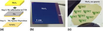
MoS2 growth in our lab using the two-step method [Fig. 1(a)] involves the room temperature deposition of parent Mo films on Si/SiO2 substrates as the first step. Mo films with different thicknesses were prepared by controlling the sputter deposition time. A high-purity (99.99%) Mo metal target of 50 mm in diameter was used for sputtering Mo thin films. The substrates were initially cleaned thoroughly with acetone in an ultrasonic bath, followed by cleaning in ethanol, methanol, and deionized (DI) water. The substrates were fixed on the heater, and the chamber was evacuated to a vacuum level of 10−7 Torr. Before every sputtering run, the target was presputtered for 5 min to ascertain the same state of Mo target for each sample. In the second step, the deposited Mo films were subsequently placed in a low-pressure CVD system (graphene square CVD) equipped with a 4 inch diameter quartz tube furnace. A ceramic boat containing pure sulfur (∼1 gm, Sigma Aldrich, St. Louis, Missouri) was placed in the upstream of the quartz tube. Argon was used as a carrier gas to convey sulfur vapor species to the Mo films. The tube was pumped down to a pressure of 10−3 Torr and flushed with Ar gas repeatedly to guarantee a favorable growth atmosphere. In the flow atmosphere of 200 sccm Ar with a chamber pressure of 5 Torr, the furnace was heated to 600 °C at the center zone in 30 min. After 60 min, the furnace was cooled down naturally to room temperature. Figures 1(b) and 1(c) show the optical images of large area MoS2 film grown on Si/SiO2 and quartz substrates, respectively. These films can be further transferred to any arbitrary substrates using KOH solution and DI water. The sample names S1, S2, S3, S4, and S5 are used for Mo films deposited for 4, 10, 30, 60, and 180 s, respectively.
(a) Schematic showing the two-step growth method; Step 1: Deposition of Mo film using magnetron sputtering, Step 2: Sulfurization of Mo films in a CVD furnace. Large area growth of MoS2 on (b) Si/SiO2 and (c) transparent (quartz) substrate.

B. Characterization of grown MoS2 film
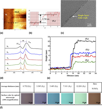
MoS2 films synthesized by using the two-step method were characterized to confirm their thickness, crystalline quality, and uniformity over the wafer scale. Figures 2(a) and 2(b) show the atomic force microscopy (AFM) image and corresponding height profile of MoS2 film for sample S1. A step height of 0.728 nm infers the presence of SL MoS2. To further confirm the thickness, cross-sectional high resolution transmission electron microscopy (HRTEM) image was recorded as shown in Fig. 2(c). However, the HRTEM image represents a SL MoS2 thickness, but the film was not uniform over the entire region of the cross-section. The formation of voids or breakage as seen in the image could be attributed to very low sputter deposition time and polycrystalline nature of the MoS2 film. Raman spectroscopy is an excellent tool to address the evolution of structural properties in layered materials changing their thickness from the 3D bulk to 2D van der Waal layered structures. Reference Bromley16 The Raman spectrum of bulk MoS2 has two vibration modes: an in-plane (E2g) mode located around 383 cm−1 and an out-of-plane (A1g) mode, which is located at 407 cm−1. The difference of frequencies between these two modes could be used to identify the number of layers in MoS2 films. Figure 2(d) shows the Raman spectra of MoS2 films with different thicknesses, measured at 532 nm excitation laser line. A frequency difference (Δk) of ∼19.7 cm−1 observed in sample S1 confirms a SL MoS2, Reference Mak, Lee, Hone, Shan and Heinz17 whereas this frequency difference rises with increasing number of layers, indicating the modulation of MoS2 film thickness. The thickness of the MoS2 film corresponding to sample S2, S3, S4, and S5 as estimated by AFM height profile measurements was found to be 3.38, 5.48, 7.11, and 12.20 nm, respectively [Fig. 2(e)]. We also developed a simple and nondestructive method to identify the number of MoS2 layers by using the optical contrast of thickness modulated MoS2 films. The detail study of this method is published elsewhere. Reference Park, Choudhary, Smith, Lee, Kim and Choi18 Figure 2(f) shows the optical images of MoS2 films grown on Si/SiO2 substrate taken by Nikon Eclipse ME600 microscope (Melville, New York). It is to be noted that the color of MoS2 film changes from purple to green with increasing number of MoS2 layers. The change in MoS2 color could be due to the change in optical band gap energy and reflectance with changing thickness. Reference Yim, O'Brien, McEvoy, Winters, Mirza, Lunney and Duesberg19 The facile optical contrast and color methods of thickness identification could be applied to a variety of substrate systems. The detail method for identifying MoS2 thickness on different substrate systems is under investigation.
MoS2 characterization fabricated by two-step method (a) AFM image and (b) height profile of MoS2 film on SiO2 substrate (sample S1), (c) cross-section HRTEM image of S1 showing voids and discontinuous film, (d) Raman spectra of MoS2 film with different thicknesses. Peaks shifts apart with increasing thickness, (e) AFM height profiles of MoS2 films with different thicknesses (S2–S5), and (f) optical images showing the color variation in MoS2 films with increasing thickness from sample S1 to S5.

C. Field effect transistors
One of the most important application for semiconducting MoS2 is in FETs for next generation electronic devices. Reference Yoon, Park, Bae, Kim, Jang, Hyun, Lim, Kahng, Hong and Lee20 There have been several efforts in fabricating MoS2 FETs using mechanical exfoliation and CVD methods but the mobility on SiO2 substrates is typically characterized at low value of 0.01–10 cm2/(V s). Reference Li and Li21,Reference Zhan, Liu, Najmaei, Ajayan and Lou22 Radisavljevic et al. Reference Radisavljevic, Radenovic, Brivio, Giacometti and Kis6 used HfO2 gate dielectric for SL MoS2 transistor and reported an outstanding mobility of 200 cm2/(V s) and current on/off ratio of 1 × 10⁸ at room temperature. However, the fabrication of MoS2 FET devices by using above methods resulted in non-uniform small flakes without any control over the film thickness. Therefore, it is imperative to develop new fabrication methods for scalable and layered controlled synthesis of MoS2 films for commercial electronics applications.
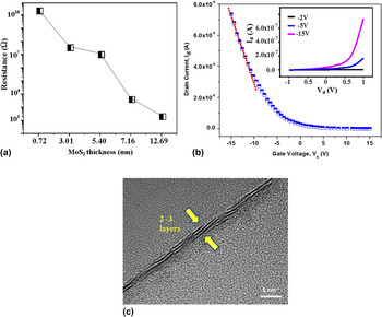
The wafer scale and thickness modulated MoS2 films fabricated by using our two-step method were characterized for electrical performance. Figure 3(a) shows the variation of electrical resistance with increasing MoS2 film thickness, measured at room temperature. It could be observed from the graph that sample S1 shows very high resistances while the resistance decreases with increasing MoS2 thickness (S2 & S3) and shows a metallic conductance for thicker MoS2 films (S4 & S5). The very high resistance in sample S1 could be attributed to the discontinuity or void formation and large spatial constraints imposed by the underlying substrate. The electrical measurement for this sample did not show any FET behavior. However, a good FET behavior with p-type conduction was observed in sample S2 as shown in Fig. 3(b). The mobility and current I on/off recorded for sample S2 were ∼12.24 cm2/(V s) and ∼1.56 × 10⁶, respectively. Reference Choudhary, Park, Hwang and Choi23 Our results are better than many previous reports on mechanically exfoliated and CVD grown MoS2 atomic layers. Generally, most of the MoS2-based FETs showed n-type behavior but the origin of the electron doping is still unclear and need more investigation. On the other hand, there are only few studies showing a p-type conduction in MoS2. Reference Zeng, Yin, Huang, Li, He, Lu, Boey and Zhang24 We believe that the p-type behavior might have originated from the localized trap states that are expected to be present at the interface of the Si/SiO2 substrate and MoS2 film, which tends to relocate the Fermi level of the SiO2/MoS2 system just below the valence band maxima, making the system a p-type semiconductor. For higher MoS2 thickness (12.29 nm), a conducting electrical behavior with a high value of drain current was observed in the FET measurements. It could be attributed to the presence of unsulfurized Mo films at MoS2-substrate interface. Hence, there is a critical thickness limit upto which Mo can be fully sulfurized by using the same set of experimental conditions. Figure 3(c) shows the cross-section image of MoS2 film from sample S2 demonstrating high uniformity and complete sulfurization of the Mo film.
(a) Electrical resistance of MoS2 film with varying thickness, (b) FET properties shown by sample S2, and (c) HRTEM cross-section of 2–3 layers MoS2, indicating a complete sulfurization and uniform MoS2 growth.

III. MoS2 FOR ENERGY APPLICATIONS
A. MoS2 film growth by direct deposition
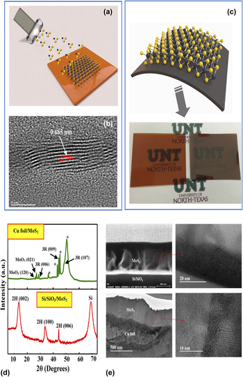
2D MoS2 also has been attracted as a promising supercapacitor electrode material due to its intriguing sheet-like structure that provides large surface area for double layer charge storage and the presence of multiple oxidation states in the Mo atom facilitating pseudocapacitance by the intercalation of electrolyte ions (H+; Li+) into S–Mo–S nanosheets. However, relatively thick films are needed for the sufficient charge storage and for the reliable performance of the material. Reference Yang, Fei, Ruan, Xiang and Tour25 We found that the direct deposition of MoS2 by sputtering is an efficient method to make a desired structure of MoS2 for a large scale supercapacitor electrode on any substrate including flexible substrates. Hence, we fabricated a flexible MoS2 thin film electrode and characterized its performance in supercapacitor. It is also noted that this method offers the possibility of MoS2 deposition on complex surfaces with high uniformity on larger cross-section and better adhesion as compared to previously reported results on chemically exfoliated or CVD grown films. In addition, these methods are accompanied with residues and contaminants. Figure 4(a) shows the schematic of MoS2 deposition directly on various substrates including Cu foil, Si/SiO2, and polyimide. The MoS2 films were deposited at low substrate temperature of 300 °C by direct sputtering of MoS2 target (99.8% purity) at a radio frequency (RF) power of 60 W in an inert gas plasma (Argon ∼99.999% purity).
(a) Schematic diagram showing the direct sputter deposition of MoS2 films, (b) HRTEM image clearly shows the formation of high quality MoS2 film by sputtering method, (c) schematic diagram showing the potential of direct deposition on flexible substrates. Camera images demonstrating MoS2 film grown on polyimide substrate in our lab, (d) XRD patterns revealing 2H and 3R MoS2 structure in MoS2 films deposited on Si/SiO2 substrate and Cu foil, respectively (peaks shown by asterisk are from Cu substrate), and (e) cross-sectional HRTEM and morphology of MoS2 film on Si/SiO2 and Cu substrates.

B. Characterization of direct deposited MoS2 films
Although, there are several studies in the past that utilized sputtering to deposit MoS2 coatings for solid lubricant applications, Reference Christy26 the reports on the fabrication of MoS2 films for electronics and energy applications by direct sputtering are sparse. Voevodin and co-workers Reference Muratore, Hu, Wang, Haque, Bultman, Jespersen, Shamberger, McConney, Naguy and Voevodin27 attempted to grow 3–6 molecular layers of MoS2 on thermally grown silicon oxide and (002) graphite using magnetron sputtering at a growth temperature of only 350 °C. In another study, Alam et al. Reference Alam, Wang, Pulavarthy, Haque, Muratore, Glavin, Roy and Voevodin28 studied the dependence of grain size on temperature by in situ heating of free standing MoS2 in transmission electron microscopy. In this context, our research group succeeded in fabricating high quality, large scale MoS2 films on different substrates by using direct sputtering technique. The HRTEM image of Fig. 4(b) demonstrates the formation of high quality MoS2 films on Cu foil. The thickness of individual layer was found to be 0.685 nm, which is the typical thickness of SL MoS2. Reference Yu, Li, Liu, Su, Zhang and Cao29 The possibility of low temperature deposition (∼300 °C) enabled us to grow MoS2 layers on other flexible substrates like polyimide [Fig. 4(c)]. Interestingly, we found that MoS2 films deposited on different substrates exhibited different crystal structures. It is clear from the X-ray diffraction (XRD) spectra of Fig. 4(d) that MoS2 films grown on Si/SiO2 substrates exhibited a hexagonal (2H) phase while a rhomobohedral (3R) phase was indexed by the XRD results when MoS2 was deposited on Cu foil. The formation of different crystalline structures in our MoS2 films could be attributed to the fact that the crystalline structure of sputtered deposited MoS2 films depends on the chemically active sites, surface smoothness, and roughness of the substrates. Reference Bertrand30 In our case, SiO2 surface is much smoother as compared to the Cu foil and therefore possess high chances of layered structure growth (2H) parallel to the substrates. On the other hand, the uneven morphology in Cu foil with large surface roughness may promote the growth of nanoclustered MoS2 films in highly un-equilibrium conditions and leads to a less stable (3R) polytype. Figure 4(e) shows the HRTEM cross-section and morphology of MoS2 film on Si/SiO2 and Cu substrates, respectively. It is observed that MoS2 film crystallized into a well layered (2H) structure on Si/SiO2 while a random distribution of MoS2 layers with a un-equilibrium structure is formed on Cu foil, which is consistent with the XRD results.
C. MoS2 for supercapacitors
The MoS2 films deposited on Cu foil were used as supercapacitor electrode and its electrochemical performance was evaluated by using cyclic voltammetry (CV). Charge storage in MoS2 thin films can be done by three ways: (a) double layer charge storage by individual interlayer of MoS2, (b) intra S–Mo–S double layer charge storage due to diffusion of electroactive species into the basal plane, and (c) Faradic charge transfer due to several oxidation states of Mo atoms ranging from +2 to +6 exhibiting pseudocapacitance due to efficient intercalation of alkali ions (H+, Li+, Na+, and K+). Reference Soon and Loh31,Reference Choudhary, Patel, Ho, Dahotre, Lee, Hwang and Choi32
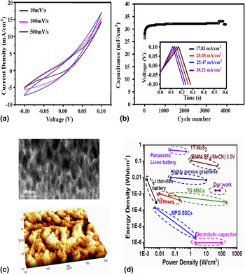
Figure 5(a) shows the CV results of our MoS2 electrode at different scan rates ranging from 10 mV/s to 500 mV/s. The elliptical S-shape curve of the CV indicates the combination of double layer charge storage and pseudocapacitance mechanism in our electrode. Reference Alam, Wang, Pulavarthy, Haque, Muratore, Glavin, Roy and Voevodin28 The observed deviation from the ideal rectangular characteristics is mainly attributed to large polarization of electrode and physical/chemical adsorption at the interface. Furthermore, galvanostatic charge/discharge tests were performed at a current density of 25.47 mA/cm2. An excellent electrochemical performance with a capacitance of ∼30 mF/cm2 and cyclic stability up to 4000 cycles could be observed in Fig. 5(b). The existence of linear and triangular charge/discharge profile at different current densities [inset of Fig. 5(b)] represents the dominance of double layer charge storage mechanism. A small equivalent series resistance of only ∼3 Ω was also calculated from the Nyquist plot of our electrodes (not shown here). The excellent electrochemical performance observed in our MoS2 electrodes could be attributed to the open porous structure with a 3D MoS2 island structure shown by the HRTEM and AFM image of the top surface of the MoS2 film [Fig. 5(c)]. This unique structure facilitates ample open channels for the large ion transport and penetration of electrolytic ions into the pores leads to high capacitive performance. Figure 5(d) compares the volumetric power and energy densities of our MoS2 electrode with other commonly used power sources. It is observed that the power density of our supercapacitor electrode (∼80 W/cm3) surpasses the previously reported values and the volumetric energy density (1.62–2.33 mWh/cm3) exceeds conventional activated carbon and electrolytic capacitors. The interesting electrochemical properties of MoS2 film makes it attractive as a promising electrode for the next generation supercapacitor energy storage devices.
(a) CV curves at different scan rates in 0.5 M H2SO4 electrolyte, (b) capacitance variation with cycle number a current density of 25.47 mA/cm2. The inset shows the charge–discharge profiles at different current densities, (c) AFM and HRTEM image showing the formation of unique 3D porous MoS2 structure, and (d) Ragone plot showing comparing the energy and power density of our supercapacitor electrode with different supercapacitor electrodes.

IV. CONCLUSIONS
The present studies explore the growth of large scale MoS2 thin films for potential applications in electronics and energy storage devices. The two-step sputtering-CVD and direct deposition by magnetron sputtering methods were developed to grow large scale, uniform, and thickness modulated MoS2 films. Raman, AFM, and HRTEM techniques were used to confirm the uniformity and atomic layered structure of MoS2 films. FET measurements on our MoS2 films grown by two-step method exhibited a high field effect mobility and current on/off ratio. High performance supercapacitor electrodes exhibiting high capacitance (∼30 mF/cm2) and long cyclic stability were fabricated using the direct deposition of MoS2 films on Cu foils. Direct deposition by sputtering offers an advantage for wafer scale MoS2 films growth directly on flexible substrate. The current approaches of large scale MoS2 deposition with interesting results will definitely trigger important technological advancement taking MoS2 film from the laboratory to industrial applications.