Introduction
Solar energy harvesting through photovoltaic conversion has gained attention as a sustainable and environmentally friendly solution for meeting the rapidly increasing global energy demand. The high cost of solar-cell technology, however, limits its widespread use. This situation has generated considerable interest in developing alternative solar-cell technologies that reduce cost through the use of less expensive materials and processes.
Dye-sensitized solar cells (DSSCs) Reference O’Regan and Grätzel1 and organic photovoltaics (OPV) Reference Brabec, Gowrisanker, Halls, Laird, Jia and Williams2 have been intensively studied in the last decade as cost-effective solar cells. An alternative route to low-cost production is to combine the advantages of inorganic and organic materials with a nanostructured device architecture. We have reported a nanostructured Sb2S3/P3HT (poly-3-hexylthiophene) inorganic/organic heterojunction hybrid solar cell by integrating the key features of DSSCs for the nanostructured architecture and OPV for organic hole transporting materials. Reference Chang, Rhee, Im, Lee, Kim, Seok, Nazeeruddin and Grätzel3 An important advantage is the ability to tailor the bandgap by modifying the molecular properties or the composition. We can choose architectures based on light harvester properties, such as absorption coefficient, exciton diffusion length, and purity. In DSSCs, dyes, used as light absorbers, with a relatively low absorption coefficient need nanostructured mesoporous electrodes to increase the amount of dye loaded onto the photoelectrode. Organic materials that have short charge-diffusion lengths are beneficial for nanostructured architecture. We also need to consider factors such as cell architecture, process, and materials to fabricate efficient solar cells.
Recently, inorganic–organic hybrid perovskite solar cells (PSCs) have shown great potential as a low-cost and high-performance photovoltaic technology, owing to the effective combination of the solution-casting process and its unique material properties. Since the first report of CH3NH3PbX3 (X = Br, I) as an alternative to a light harvester in a dye-sensitized configuration with a mesoporous titanium dioxide (TiO2) template, Reference Kojima, Teshima, Shirai and Miyasaka4 significant progress in solar-cell performance has been made by several groups. Reference Kim, Lee, Im, Lee, Moehl, Marchioro, Moon, Humphry-Baker, Yum and Moser5–Reference Burschka, Pellet, Moon, Humphry-Baker, Gao, Nazeeruddin and Grätzel8 We have recorded important milestones in improving the efficiencies of PSCs. This review describes steps for fabricating efficient PSCs, as their performance is mainly governed by device architecture, deposition process for perovskite layers, and junctions between key components. In particular, we emphasize the importance of the mediator retarding rapid reaction, which prevents the formation of extremely uniform and dense perovskite layers between organic cations and PbI2.
Step 1: Noble architecture for perovskite solar cells
Solar cells require several basic operations to directly convert sunlight into electricity. Optoelectric materials absorb photons of light and separate charge carriers of electron–hole pairs, or excitons, and release these carriers to an external circuit under an established internal voltage.
To fabricate efficient solar cells, high-purity materials, which are very expensive, are needed to extract carriers without significant recombination. On the other hand, a sensitized-type solar cell, which utilizes narrow bandgap materials to sensitize wide bandgap oxide semiconductor materials, can use relatively impure materials due to its unique cell architecture in which light absorption, electron transport, and hole transport are performed in different materials in contrast to conventional solar cells such as crystalline Si, CdTe, and CIGS solar cells. Sensitization by dyes as light absorbers is a typical and successful example of sensitized-type solar cell. Reference O’Regan and Grätzel1
In DSSC, a relatively low light absorption coefficient of organic dye molecules is one of the limiting factors to further improving photovoltaic performance. Inorganic semiconductors such as CdS(e), PbS(e), and Sb2S(e)3 with high extinction coefficients have been used as an alternative light absorber. Reference Chang, Rhee, Im, Lee, Kim, Seok, Nazeeruddin and Grätzel3,Reference Vogel, Hoyer and Weller9–Reference Lee, Chen, Moon, Sauvage, Sivula, Bessho, Gamelin, Comte, Zakeeruddin and Seok12 Miyasaka et al. first applied methylammonium lead iodide (MAPbI3) and methylammonium lead bromide (MAPbBr3) perovskites as light sensitizers in mesoporous (mp)-TiO2-based sensitized solar cells. Reference Kojima, Teshima, Shirai and Miyasaka4 The improved efficiencies of 3.8% in 2009 and 6.5% in 2011 were meaningful, but an extreme instability of perovskite materials to liquid electrolytes was a big obstacle at that time. Reference Kojima, Teshima, Shirai and Miyasaka4,Reference Im, Lee, Lee, Park and Park13
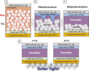
We have studied solid-state inorganic–organic hybrid solar cells that employ inorganic sensitizers such as Sb2S3, PbS, and organic semiconductors such as P3HT (poly-3-hexylthiophene), PCPDBT (poly-[2,1,3-benzothiadiazole-4,7-diyl[4,4-bis(2-ethylhexyl)-4H-cyclopenta[2,1-b:3,4-b′]dithiophene-2,6-diyl]]), and PCDTBT ((poly-[[9-(1-octylnonyl)-9H-carbazole-2,7-diyl]-2,5-thiophenediyl-2,1,3-benzothiadiazole-4,7-diyl-2,5-thiophenediyl])). These are based on mp-TiO2 sensitized solar cells to improve power conversion efficiency and to avoid the problem of liquid DSSCs. Reference Chang, Rhee, Im, Lee, Kim, Seok, Nazeeruddin and Grätzel3,Reference Im, Lim, Chang, Lee, Maiti, Kim, Nazeeruddin, Grätzel and Seok14–Reference Chang, Im, Lee, Kim, Lim, Heo and Seok16 The high extinction coefficient of inorganic semiconductors allowed reduced thickness of the mp-TiO2 layer to under 1 µm and consequently allowed the use of a P3HT semiconducting polymer as a hole transporting material (HTM), as shown in Figure 1 a.
Evolution of cell architecture: (a) solid-state Sb2S3-sensitized solar cell, Reference Chang, Rhee, Im, Lee, Kim, Seok, Nazeeruddin and Grätzel3 (b) pillared perovskite solar cell, Reference Heo, Im, Noh, Mandal, Lim, Chang, Lee, Kim, Sarkar and Nazeeruddin7 and (c) bilayered perovskite solar-cell architectures. Reference Jeon, Noh, Kim, Yang, Ryu and Seok21 (d) n-i-p and p-i-n cell architectures. Reference Seo, Park, Kim, Jeon, Noh, Yoon and Seok27,Reference Ryu, Noh, Jeon, Kim, Yang, Seo and Seok28 Representative materials are inserted in parentheses. Note: HTM, hole transporting material; P3HT, poly(3-hexylthiophene); Bl, barrier layer; FTO, fluorine-doped tin oxide; PTAA, poly-triarylamine; mp, mesoporous; ITO, indium-doped tin oxide; PEDOT:PSS, poly(3,4-ethylenedioxythiophene) polystyrene sulfonate; PCBM, [6,6]-phenyl-C61-butyric acid methyl ester. Adapted from References 3, 7, 21, 27, and 28.

In particular, the hybridization of an inorganic light absorber and organic hole transporter offered a novel direction for achieving high-efficiency solid-state solar cells. Reference Chang, Rhee, Im, Lee, Kim, Seok, Nazeeruddin and Grätzel3 The inorganic–organic hybrid solar cell overcomes the instability problem of the liquid perovskite-sensitized solar cell by introducing solid-state HTMs. In addition, the intimate interaction of the inorganic sensitizer and functional moieties in the HTM are crucial factors to minimize energy loss in the inorganic–organic hybrid solar cells. Reference Im, Lim, Chang, Lee, Maiti, Kim, Nazeeruddin, Grätzel and Seok14 Based on this background, we investigated photovoltaic performance of inorganic–organic hybrid solar cells fabricated using MAPbI3 as light harvesters on mp-TiO2 and several hole-conducting materials such as P3HT, PCPDTBT, PCDTBT, and PTAA (poly-triarylamine). Reference Heo, Im, Noh, Mandal, Lim, Chang, Lee, Kim, Sarkar and Nazeeruddin7 In contrast to Sb2S3, PTAA showed superior photovoltaic performance compared to other HTMs, including the thiophene moiety.
Although the motivation was to replace Sb2S3 with MAPbI3 in the hybrid solar cell, the resulting cell architecture with perovskite was completely different from conventional sensitized-type solar cells. MAPbI3 was not only coated on the surface of TiO2 nanoparticles, but also packed into pores in the mp-TiO2 layer and formed as a partial thin film on the mp-TiO2 layer. We call this architecture a pillared structure consisting of a three-dimensional composite layer of TiO2/MAPbI3 and an incomplete MAPbI3 overlayer. Reference Heo, Im, Noh, Mandal, Lim, Chang, Lee, Kim, Sarkar and Nazeeruddin7
Figure 1b shows the detailed structure of the pillared architecture. Reference Heo, Im, Noh, Mandal, Lim, Chang, Lee, Kim, Sarkar and Nazeeruddin7 In contrast to solid-state perovskite-sensitized solar cells Reference Kim, Lee, Im, Lee, Moehl, Marchioro, Moon, Humphry-Baker, Yum and Moser5 and meso-superstructured solar cells, Reference Lee, Teuscher, Miyasaka, Murakami and Snaith6 which work by hole transport through a spiro-OMeTAD (2,2′,7,7′-tetrakis(N,N-di-p-methoxyphenylamine) 9,9′-spirobifluorene) network that infiltrated the pores of MAPbI3 deposited within the mp-layer, the pillared structure does not allow HTM infiltration into mp-TiO2 pores because the pores are already filled with MAPbI3. The high power conversion efficiency (PCE) value of 12% obtained in the pillared structure Reference Heo, Im, Noh, Mandal, Lim, Chang, Lee, Kim, Sarkar and Nazeeruddin7 suggested that the working mechanism of hole transport through the perovskite itself is useful in further improving the PCE in PSCs.
The ambipolar charge transport properties of MAPbI3 explain how both the pillared structure and meso-superstructure cells work well. Many studies demonstrated how generated excitons instantly separate into free carriers of electrons and holes in MAPbI3 and that the electrons and holes show similar diffusion lengths. Reference Lin, Armin, Nagiri, Burn and Meredith17–Reference D’Innocenzo, Grancini, Alcocer, Kandada, Stranks, Lee, Lanzani, Snaith and Petrozza19 The ambipolar property allows a planar-type architecture consisting of TiO2 film/MAPbI3 film/HTM film, and planar PSCs were reported by depositing MAPbI3 using vacuum thermal evaporation. Reference Liu, Johnston and Snaith20 The high PCE obtained for both the pillared structure and the planar PSC revealed that a compact MAPbI3 thin film was a key factor in improving the PCE. We successfully fabricated uniform and flat MAPbI3 films through solvent engineering in the solution process, discussed later in this article. Reference Jeon, Noh, Kim, Yang, Ryu and Seok21 However, the planar MAPbI3 cell showed significant hysteresis of the current-voltage curve and reduction of power with increasing delay time. Over-estimation of the PCE, due to large hysteresis in the current–voltage curves, and unreliable power generation for initial PSC development have been critical issues.
The introduction of a mp-TiO2 layer was an excellent solution to remove the hysteresis and unreliable PCE issues. Consequently, a bilayer structure consisting of a 3D composite layer of TiO2/MAPbI3 and a complete MAPbI3 overlayer by extension of the pillared structure yielded a reliable PCE of 16.5% (Figure 1c). Reference Jeon, Noh, Kim, Yang, Ryu and Seok21 The origins of the hysteresis and unreliable PCE in PSCs remain controversial; ferroelectricity due to the dipoles of methylammonium molecules, ion migration, and unbalanced charge collection rate have been suggested. Reference Snaith, Abate, Ball, Eperon, Leijtens, Noel, Stranks, Wang, Wojciechowski and Zhang22–Reference Jeon, Noh, Yang, Kim, Ryu, Seo and Seok26 Among these, unbalanced charge collection that depends on cell architecture, perovskite material, and selective n/p-type contact layers are the most influential, as indicated by recently reported results.
PSCs can be structurally classified into two architectures (n-i-p and p-i-n structures), as shown in Figure 1d. Reference Seo, Park, Kim, Jeon, Noh, Yoon and Seok27,Reference Ryu, Noh, Jeon, Kim, Yang, Seo and Seok28 Referencing the incident direction of sunlight and assuming that perovskite is an intrinsic semiconductor for convenience, n-i-p and p-i-n architectures indicate cell structures where light enters through the n-type and p-type layers, respectively, The generated electrons and holes show opposite distribution in n-i-p or p-i-n cell architectures; charge collection behavior is also different. The fact that the p-i-n planar architecture using MAPbI3 does not show hysteresis, while the n-i-p planar architecture shows significant hysteresis, indicates that the hysteresis can be attributed to the cell architecture rather than MAPbI3 itself. Reference Jeon, Noh, Kim, Yang, Ryu and Seok21,Reference Seo, Park, Kim, Jeon, Noh, Yoon and Seok27
In addition to cell architecture, the charge transfer rate between perovskite and selective n/p-type contact layers can also influence the balance of charge collection. Unbalanced charge collection is probably related to the electrical character of the perovskite materials and charge accumulation at the interface between the perovskite and n-type/p-type layers. Therefore, control of the electrical character for perovskites, interfacial engineering, and development of new n-type and p-type materials is important to further improve PCE in PSCs. In addition, design of cell architecture considering the charge transfer rate from perovskite to n/p-type materials will be required to balance electron and hole collection in high-efficiency perovskite cells.
Step 2: Processes for efficient PSCs
The evolution of cell architecture requires the perovskite layer to be as uniform, flat, and thin as possible. To control the morphology of the perovskite, the self-assembly crystallization properties of inorganic–organic hybrid halide perovskites should be managed, due to the strong ionic interactions between the cations and halogen anions. The strong self-assembly ability during solvent evaporation, therefore, does not allow for the perovskite to form compact and flat film in the solution process.
Thus, strategies to control the rapid crystallization behavior of such perovskites are necessary. Sequential deposition is one of the strategies to form a film by pre-deposition of PbI2 and sequential reaction to MAI. Reference Burschka, Pellet, Moon, Humphry-Baker, Gao, Nazeeruddin and Grätzel8,Reference Im, Jang, Pellet, Grätzel and Park29,Reference Chen, Zhou, Hong, Luo, Duan, Wang, Liu, Li and Yang30 However, formation of perovskite crystals by nucleation and growth on the surface of the PbI2 layer limits formation of high-quality films that have a flat surface and complete coverage. Another strategy is to retard the crystallization kinetics. The first report on the retardation approach was based on the solvent engineering process. Reference Jeon, Noh, Kim, Yang, Ryu and Seok21 Because the rapid crystallization behavior is attributed to the strong ionic interaction between cations and halogen anions, appropriate inhibitors can retard crystallization into perovskite during the solution process.
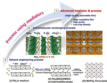
In the solvent engineering process, the compact and flat MAI-PbI2-DMSO (dimethylsulfoxide) complex film is first formed on a substrate by dripping a non-solvent, such as toluene and ether, during the spin-coating process that uses MAPbI3 dissolved in γ-butyrolactone (GBL)-DMSO solution. The crystalline MAI-PbI2-DMSO intermediate phase converts to the pure MAPbI3 perovskite phase upon removal of DMSO through thermal annealing. Such a solid-state phase transformation leads to an extremely homogeneous, flat perovskite film with a well-developed grain structure. Reference Jeon, Noh, Kim, Yang, Ryu and Seok21 In the solvent engineering process, DMSO plays a decisive role as a mediator rather than just an inhibitor. As shown Figure 2 , DMSO prevents direct reaction between MAI and PbI2 through the formation of a crystalline MAI-PbI2-DMSO intermediate phase, which produces the MAPbI3 perovskite phase. The mediator, such as DMSO, is a key factor in controlling the crystallization kinetics to produce a high-quality perovskite film. Recently, other inhibitors such as 1,8-diiodooctane (DIO), hydriodic acid (HI), and N-cyclohexyl-2-pyrrolidone (CHP) have been reported as mediators. Reference Liang, Liao, Chueh, Zuo, Williams, Xin, Lin and Jen31–Reference Jeon, Lee, Kang, Kim, Yeo, Lee, Kim, Yun and Kim33
Processes using mediators to control rapid self-assembly crystallization and to further improve the quality of the perovskite film: (a) solvent engineering process Reference Jeon, Noh, Kim, Yang, Ryu and Seok21 and (b) intramolecular exchanging process Reference Yang, Noh, Jeon, Kim, Ryu, Seo and Seok34 are represented as successful examples; and (c) an advanced mediator and process will be needed to deposit high-quality perovskite films. Adapted from Reference 27. Note: DMSO, dimethylsulfoxide; FA, formamidinium; MA, methylammonium; FAI, formamidinium iodide.

For further improvement of perovskite photovoltaic performance, advanced mediators or advanced processes using novel mediators need to be developed to achieve the following functionalities beyond mere formation of a compact film: (1) The mediator/process should convert the pre-perovskite phase to the perovskite phase at any designed time and condition; (2) the mediator/process should reduce defects and enhance crystallinity in the resulting perovskite phase; and (3) the mediator/process should be extended to a large-scale and high-speed process.
We recently proposed an advanced process via a DMSO mediator for high-quality FAPbI3 thin films. Reference Yang, Noh, Jeon, Kim, Ryu, Seo and Seok34 In contrast to a retardation concept for the formation of MAPbI3 perovskite from the MAI-PbI2-DMSO intermediate phase, we introduced an immediate exchanging reaction of formamidinium iodide (FAI) with DMSO in a pre-deposited PbI2–DMSO thin film. Due to its weak van der Waals interactions, the DMSO molecule intercalation into PbI2 can be easily replaced by external FAIs because of the FAI’s higher affinity toward PbI2 compared to DMSO. Reference Jeon, Noh, Kim, Yang, Ryu and Seok21,Reference Miyamae, Numahata and Nagata35 As shown in Figure 2b, highly uniform and dense pre-deposited PbI2-DMSO layers could be directly converted to FAPbI3 through crystallization by the intramolecular exchange process (IEP) of DMSO intercalated in PbI2 with FAI, resulting in a highly uniform and compact formamidinium lead iodide (FAPbI3) thin film. In addition, the IEP following Equation 1 does not induce large volume expansion, unlike the FAPbI3 formed with FAI intercalating into pristine PbI2 because the molecular sizes of DMSO and FAI are similar. As a consequence, an IEP-derived FAPbI3 film shows a large grain structure of around 1 μm and (111) preferred crystallographic orientation without any secondary phase at even a high thickness (∼550 nm) to absorb light up to wavelengths of 800 nm:
 $$Pb{I_2} - DMSO + FAI\, \to \,Pb{I_2} - FAI + DMSO \uparrow (removal).$$
The high-quality FAPbI3-based solar cells show certified PCEs of 20.1%, Reference Yang, Noh, Jeon, Kim, Ryu, Seo and Seok34 which is the best certified value for PSCs at present. In addition to high PCE, the IEP shows a high degree of reproducibility and is simple to extend to large-area and high-speed processes for commercialization.
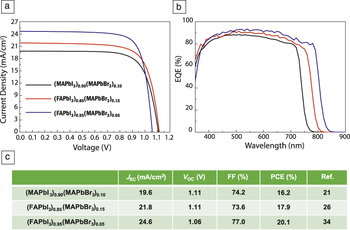
The development of an advanced process for high-quality and thick (550 nm) FAPbI3 perovskite films is significant because FAPbI3 has advantages such as a smaller bandgap of 1.47 eV, hysteresis-less property for the n-i-p cell architecture, Reference Jeon, Noh, Yang, Kim, Ryu, Seo and Seok26 and superior stability compared to MAPbI3. Reference Eperon, Stranks, Menelaou, Johnston, Herz and Snaith32 Because the smaller bandgap generally requires a thicker film to absorb sufficient solar light, perovskites with an optimal bandgap of 1.4 eV or 1.1 eV, based on the Shockley–Queisser limit, need to be thicker than 550 nm. Reference Shockley and Queisser36 A reduction in the bandgap for light harvesting is an important strategy for improving the PCE in PSCs. Figure 3 shows certified current density-voltage (J–V) curves and external quantum efficiency (EQE) spectra of PSCs since 2013, revealing the bandbap reduction successfully leading to improvement of the PCE. (MAPbI3)1–x (MAPbBr3) x at x = ∼ 0.1 in the bilayer architecture cell showed a high certified PCE of 16.2% in 2013, but its bandgap of ∼1.60 eV was too wide to maximize the PCE based on the Shockley–Queisser limit. Reference Jeon, Noh, Kim, Yang, Ryu and Seok21
(a) The current density–voltage (J–V) curves of the highest performing Korea Research Institute of Chemical Technology perovskite cells since 2013 and (b) their external quantum efficiency (EQE) spectra. Reference Jeon, Noh, Kim, Yang, Ryu and Seok21,Reference Jeon, Noh, Yang, Kim, Ryu, Seo and Seok26,Reference Yang, Noh, Jeon, Kim, Ryu, Seo and Seok34 (c) The photovoltaic parameters are summarized. J–V curves and parameters were obtained by averaging reverse and forward sweeps to avoid overestimation due to hysteresis. The introduction of FAPbI3 resulted in an increase of J sc due to broad absorption of solar light. Note: J sc, short-circuit current density; V oc, open-circuit voltage; FF, fill factor; PCE, power conversion efficiency. Adapted from References 21, 26, and 34.

A reduction in bandgap for MAPbI3 has been reported by cation substitution (FA+ or Sn2+), as demonstrated by the smaller bandgaps of FAPbI3 (1.47 eV) and MASnI3 (1.2 eV). Reference Pellet, Gao, Gregori, Yang, Nazeeruddin, Maier and Grätzel37,Reference Ogomi, Morita, Tsukamoto, Saitho, Fujikawa, Shen, Toyoda, Yoshino, Pandey and Ma38 Although the bandgap of MAPbI3 can be tuned by Sn-substitution, improvements in PCE have not been demonstrated, probably due to the unstable oxidation state of Sn2+/4+ ions. In addition, although FAPbI3, with a smaller bandgap than MAPbI3, has the potential to increase the PCE, the photovoltaic performance of FAPbI3-based cells is lower than that of MAPbI3. This is because the fabricated FAPbI3 film was not compact and flat and had low crystallinity. Another disadvantage when using FAPbI3 is the formation of a yellow non-perovskite polymorph phase, which reversibly changes into a black perovskite phase.
Recently, the performance of FAPbI3 solar cells was significantly improved by stabilization of the FAPbI3 perovskite phase through composition engineering and the demonstration of a high-quality film through IEP using a DMSO mediator. Reference Jeon, Noh, Yang, Kim, Ryu, Seo and Seok26,Reference Yang, Noh, Jeon, Kim, Ryu, Seo and Seok34 For further improvements in the PCE and long-term stability of the cells, finding an advanced mediator or process can be useful for reducing the trap density in the perovskite layer and improving perovskite interface with an n/p-type layer.
The hysteresis issue for MAPbI3 should be solved by the introduction of FAPbI3 to achieve realizable generated power in PSCs. We noticed relatively asymmetric diffusion lengths for the electron (177 nm) and hole (813 nm) in FAPbI3, different from the symmetric electron (129 nm) and hole (105 nm) diffusion lengths for MAPbI3. Reference Stranks, Eperon, Grancini, Menelaou, Alcocer, Leijtens, Herz, Petrozza and Snaith18,Reference Eperon, Stranks, Menelaou, Johnston, Herz and Snaith32 Among possible reasons for this hysteresis, unbalanced charge collection between electrons and holes during cell operation is the main one. In heterojunction PSCs, electrons and holes should be collected through the n-type electrode/perovskite interface and the perovskite/p-type electrode, respectively. The transfer of electrons and holes from perovskite to n-type and p-type layers is strongly dependent on the type of perovskite and n-type/p-type contact materials. If the transfer rates of electrons and holes are different, charges would accumulate on one side, leading to capacitance. The asymmetric charge transfer rate from FAPbI3 to n-type and p-type electrodes is probably useful for eliminating hysteresis in the n-i-p cell architecture. In fact, a hysteresis-less FAPbI3 cell was demonstrated in the fluorine-doped tin oxide (FTO)-glass/barrier layer (bl)-TiO2/mp-TiO2/FAPbI3/PTAA/Au architecture. Reference Jeon, Noh, Yang, Kim, Ryu, Seo and Seok26,Reference Yang, Noh, Jeon, Kim, Ryu, Seo and Seok34 In addition to this hysteresis-less property, FAPbI3 is more resistant to decomposition into PbI2 and FAI when exposed to heat and moisture, as compared to MAPbI3, thus yielding opportunities to develop more efficient, cost-effective, and stable heterojunction PSCs.
Considering transmittance of FTO glass, the short-circuit current density (J sc) value of 24.7 mA/cm2 in the best PSC is significantly high when using (FAPbI3)1–x (MAPbBr3) x at x = ∼0.05 with a bandgap of approximately 1.49 eV. Reference Yang, Noh, Jeon, Kim, Ryu, Seo and Seok34 If we keep the same cell architecture and use transparent conducting oxide (TCO) glass, such as FTO and indium-doped tin oxide, a key issue to resolve for further improving the PCE is how to minimize energy loss. The Shockley–Queisser limit reveals that the theoretical maximum of open-circuit voltage (V oc) is approximately 1.22 V for a light absorber with a bandgap of 1.49 eV, assuming a solar cell with a single bandgap semiconductor, where recombination of electron–hole pairs is only radiative. Reference Shockley and Queisser36 In the best cell, the actual V oc value is 1.06 V, and there is a difference of 0.16 V from the theoretical maximum. This difference is attributed to non-radiative recombination in perovskite cells and should be minimized to further improve the PCE. Reference Tress, Marinova, Inganäs, Nazeeruddin, Zakeeruddin and Graetzel39 Consequently, finding an advanced mediator and a process that can fabricate higher quality perovskite layers (Figure 2c) is a key step toward developing efficient PSCs.
Step 3: Heterojunctions in PSCs
The PSC consists of two heterojunctions, n-type layer/perovskite and p-type layer/perovskite, as shown in Figure 1d. We investigated the influence of the heterojunction between perovskite and p-type materials on the PSC voltage output. Reference Ryu, Noh, Jeon, Kim, Yang, Seo and Seok28 The voltage is determined by three materials: the n-type layer, perovskite layer, and p-type layer. Non-radiative recombination can occur at the two heterojunction interfaces and in the perovskite itself. First, making a perfect perovskite crystal film is important to reduce defects, such as dislocations, impurities, and even grain boundaries, because they can act as sources of non-radiative recombination. The device simulation expectation of high V oc >1.2 V with low trap density <1014 cm–3 in the MAPbI3 layer and experimental observation of very low trap density at approximately 109 cm–3 in a MAPbI3 single crystal grown at room temperature shows the possibility to further increase V oc through perfecting the perovskite crystalline film. Reference Liu, Zhu, Wei, Li, Lv, Yang, Zhang, Yao and Dai40,Reference Shi, Adinolfi, Comin, Yuan, Alarousu, Buin, Chen, Hoogland, Rothenberger and Katsiev41
In addition to the quality of the perovskite itself, the two heterojunctions strongly contribute to the PSC voltage output. Several factors at the heterojunctions influence the energy loss during photovoltaic operation: (1) charge transport resistance within the n/p-type layers, (2) charge transfer rate from the perovskite to n/p-type layers, (3) opposite charge blocking rate from the perovskite to n/p-type layers, and (4) interfacial imperfections between the perovskite layer and n/p-type layers that can work as the source for non-radiative recombination. To improve V oc, researchers have already attempted to manipulate the p-type materials and the interface between the perovskite and p-type layer. Reference Ryu, Noh, Jeon, Kim, Yang, Seo and Seok28,Reference Noh, Jeon, Choi, Nazeeruddin, Grätzel and Seok42–Reference Abate, Saliba, Hollman, Stranks, Wojciechowski, Avolio, Grancini, Petrozza and Snaith44 As a consequence, the V oc difference of 0.16 V from the theoretical maximum could be further reduced by the development of a high-quality perovskite material, n/p-type materials that have a high affinity to the perovskite, and interface engineering at the heterojunction.
We also investigated the effect of a well-ordered nanostructured NiO film on photovoltaic performance through pulsed laser deposition by controlling the oxygen partial pressure and the deposition time. NiO is one of the p-type conductors that show small electron affinity (∼1.8 eV) and a relatively large bandgap (∼3.4 eV). Nanostructured NiO films in devices based on a dense, nanostructured, and porous NiO layer enabled the fabrication of very efficient PSCs and suggested the importance of a slow recombination rate during the extraction and transport of the dissociated carriers. Reference Park, Seo, Park, Shin, Kim, Jeon, Shin, Ahn, Noh, Yoon, Hwang and Seok45
Summary
Inorganic–organic hybrid perovskite materials have shown evolutionary progress in achieving high efficiencies in emerging solar cells. In the several steps used for fabricating efficient PSCs, we first proposed a pillared architecture for PSCs via extension of our inorganic–organic hybrid solar-cell technology by integrating key features of DSSCs, OPVs, and nanocrystalline inorganic semiconductors. The pillared structure, comprising a perovskite-filled mp-TiO2 and an upper layer, was slightly modified to bilayer architecture by introducing a solvent engineering process to deposit very uniform and dense perovskite layers. The device performance was highly dependent on the architecture and upper layer morphology. We also described the importance of the mediator as one of the factors influencing perovskite layer morphology. Another important factor contributing to the performance of PSCs is the heterojunction based on the material selection between the perovskite layers and n/p materials.
Overall, we believe that controlled crystallization and morphology of perovskite layers via new mediators can be a key step to fabricate efficient PSCs. Furthermore, a tuned architecture and a heterojunction between the perovskite and n/p-type layer via interface engineering can enable further improvements in PCE and long-term stability of the cells.
Acknowledgments
This work was supported by the Global Research Laboratory Program, the Global Frontier R&D Program on Center for Multiscale Energy System funded by the National Research Foundation in Korea, and by the Degree and Research Center Program (2014) through the National Research Council of Science & Technology from the Ministry of Science, ICT, and Future Planning.