Introduction
Organic–inorganic hybrid perovskites based on organic ammonium lead halides have recently emerged as a promising material for the development of novel energy harvesting technologies (see the Introductory article in this issue of MRS Bulletin). While record efficiency solar cells have been obtained by solution processing of the perovskite absorber, Reference Jeon, Noh, Yang, Kim, Ryu, Seo and Seok1–Reference Nie, Tsai, Asadpour, Blancon, Neukirch, Gupta, Crochet, Chhowalla, Tretiak, Alam, Wang and Mohite4 no preferred preparation method has crystallized from the multitude of thin-film deposition processes reported so far. Solution deposition methods have the advantage of low-cost processing and are compatible with roll-to-roll fabrication. Since the degree of crystallinity and the nature of crystals in the final perovskite film strongly affect its photophysical properties, the reaction kinetics need to be rigorously controlled to maintain more consistent device performance. Reference Moore, Sai, Tan, Smilgies, Zhang, Snaith, Wiesner and Estroff5
Physical vapor deposition methods for hybrid perovskites have also emerged, leading to high-efficiency photovoltaic devices. Reference Malinkiewicz, Roldán-Carmona, Soriano, Bandiello, Camacho, Nazeeruddin and Bolink6–Reference Malinkiewicz, Yella, Lee, Espallargas, Graetzel, Nazeeruddin and Bolink11 Such techniques are widely used in the semiconductor industry on a large scale for several optoelectronics applications. They present important intrinsic advantages over solution-based methods, including high purity, compatibility with large areas, and fine control over film thickness and morphology. Importantly, vacuum methods are intrinsically additive, meaning that multilayer devices can be built without chemical modifications of the underlying layers or the use of orthogonal solvents. Additionally, the low fabrication temperature makes vacuum deposition compatible with a wide range of substrates, including flexible substrates and textiles.
In this article, we review the developed methods for the deposition of hybrid perovskite thin films, focusing on those relying, at least partially, on vacuum deposition. The characteristics of the correspondent solar cells are also discussed.
Vacuum deposition methods for hybrid perovskite thin films
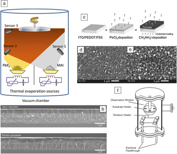
Due to the interesting semiconducting properties of organic–inorganic perovskites, their processing into thin films has been widely investigated. Reference Mitzi, Chondroudis and Kagan12,Reference Mitzi13 Era et al. demonstrated the deposition of hybrid lead iodide perovskite thin films by dual-source vapor deposition of lead iodide PbI2 and an organic ammonium iodide RNH3I (where R is an organic substituent). Reference Era, Hattori, Taira and Tsutsui14 The deposition rate and thickness were monitored using quartz oscillator microbalances (Sensors 1–3 in Figure 1 a). A wide variety of perovskite structures could be produced through this technique, including layered materials and the three-dimensional MAPbI3 (MA, methylammonium). Liu et al. also used this method to prepare the first high-efficiency planar photovoltaic devices. Reference Liu, Johnston and Snaith9 They prepared mixed halide perovskite CH3NH3PbI3−x Cl x as the absorbing layer in a planar heterojunction solar cell. Full surface coverage and uniform grain structure with large grain size were readily obtained (Figure 1b).
(a) Schematic diagram of the dual-source vapor deposition process. Heating methylammonium iodide (MAI) in vacuum results in a broader evaporating cone, affecting the reading of all sensors. Adapted with permission from Reference 6. (b) Cross-sectional scanning electron microscopy (SEM) images of completed solar cells constructed from a vapor-deposited (top) and a solution-processed perovskite film (bottom). Adapted with permission from Reference 9. (c) Scheme of the sequential vapor deposition of hybrid perovskites. Adapted with permission from Reference 7. (d) SEM image of the surface of PbI2 deposited onto ZnO thin films and (e) corresponding perovskite after dipping in MAI solution. Adapted with permission from Reference 18. (f) Scheme of a chamber used for the flash evaporation of hybrid perovskites. Reprinted with permission from Reference 26. © 1999 American Chemical Society. Note: PbX2, lead halide; PEDOT:PSS, poly(ethylenedioxythiophene) poly(styrene sulfonate); ITO, indium tin oxide.

Malinkiewicz et al. later adopted this method to deposit pure iodide CH3NH3PbI3 perovskite films. Reference Malinkiewicz, Yella, Lee, Espallargas, Graetzel, Nazeeruddin and Bolink11 In these experiments, the exact PbI2:MAI 1:1 stoichiometry (MAI, methylammonium iodide) was maintained during deposition; therefore, no annealing step was needed to fully convert the as-deposited films to the perovskite structure. Such a room temperature process is of particular interest for the deposition of hybrid perovskites onto plastic, flexible substrates. Ono et al. developed a similar method where the precursor stoichiometry is ensured by controlling the MAI vapor partial pressure inside the vacuum chamber. Reference Ono, Wang, Kato, Raga and Qi15 In this way, they were able to generate perovskite films with superior centimeter-scale uniformity.
Research toward efficient solution-processed perovskite solar cells has highlighted the importance of a fine control over the deposition parameters to obtain highly crystalline thin films. Burschka et al. developed a sequential deposition method, where the formation of the inorganic framework is decoupled from the reaction and intercalation with the ammonium halide. Reference Burschka, Pellet, Moon, Humphry-Baker, Gao, Nazeeruddin and Gratzel16 This strategy gives better control for perovskite formation and has been recently utilized in vacuum deposition processes as well. Era et al. reported thermal vacuum deposition of PbI2, followed by exposure to the organic ammonium halide vapor (Figure 1c). Reference Era, Maeda and Tsutsui17 This method has been recently adapted for the preparation of planar-heterojunction solar cells where a thin film of the PbI2 precursor was prepared by vacuum evaporation and subsequently dipped into a solution of MAI. Reference Liu, Gangishetty and Kelly18 After conversion to the perovskite, the film surface morphology is substantially altered, compared with the PbI2 layer, and composed of a closely packed collection of block-like nanocrystallites (Figure 1d–e).
A variation of this method is the evaporation/solution processing of the lead salt PbX2 (X being the halide anion) followed by the MAI reaction through chemical vapor deposition (CVD). Reference Leyden, Ono, Raga, Kato, Wang and Qi19 This process allows scalability to industrial levels, together with precise control of the gas flow rate, temperature, and pressure with high reproducibility. Chen et al. demonstrated a sequential, full vacuum evaporation process that converted in situ the sublimed PbCl2 films to perovskite upon CH3NH3I evaporation. Reference Chen, Kang, Hsiao, Yang, Chiang and Lin7,Reference Hu, Wang, Zhou, Zhang, Lv, Pang, Chen, Liu, Padture and Cui20 To achieve complete conversion of the PbCl2/MAI bilayer to a crystalline perovskite film, the PbCl2-coated substrate had to be heated during the MAI deposition such that the MAI could penetrate through and react with a 150-nm-thick layer of PbCl2. The perovskite can also be obtained through sequential deposition of alternating thin (<50 nm) PbX2/MAI multilayers, where the MAI reaction can take place in solution Reference Ng, Ren, Shen, Cheung, Gokkaya, Bai, Wang, Yang, So, Djurisic, Leung, Hao, Chan and Surya21 or in the vapor phase. Reference Chen, Chen and Dai8 This process ensures high reproducibility and layer homogeneity and appears to be compatible with large-scale production processes.
Among sequential deposition methods, it is worth mentioning the application of atomic layer deposition (ALD) in the preparation of high-quality PbI2 thin films. The deposition protocol presented by Sutherland et al. consists of ALD deposition of PbS followed by exposure to I2(g) to generate PbI2. Reference Sutherland, Hoogland, Adachi, Kanjanaboos, Wong, McDowell, Xu, Voznyy, Ning, Houtepen and Sargent22,Reference Sutherland, Hoogland, Adachi, Wong and Sargent23 Conversion to MAPbI3 is then achieved by dipping in MAI solutions. These ALD conformal coatings showed enhanced optical properties with applications in lasing element, waveguides, or optical resonators.
An alternative physical method for the deposition of hybrid perovskite thin films is flash evaporation. Reference Richards, Hart and Gallone24,Reference Saltsburg25 In this case, the perovskite is synthesized in solution, and the obtained powders are deposited onto a metal sheet and transferred to a vacuum chamber (Figure 1f). Then a large current passed through the metal sheet causing the material to rapidly evaporate and condense onto a substrate. In 1999, Mitzi et al. demonstrated that a wide range of layered organic–inorganic perovskites could be deposited with this technique (also referred to as single-source thermal ablation). Reference Mitzi, Prikas and Chondroudis26 Flash evaporation is extremely versatile since it does not depend on the composition/solubility of the material to be evaporated. Reference Chondroudis, Mitzi and Brock27–Reference Chiarella, Zappettini, Licci, Borriello, Cantele, Ninno, Cassinese and Vaglio29 Recently, Longo et al. demonstrated efficient planar heterojunction solar cells, where the photoactive MAPbI3 layer was prepared by flash evaporation of perovskite films deposited onto tantalum sheet heaters. Reference Longo, Gil-Escrig, Degen, Sessolo and Bolink30
Control over perovskite formation mechanisms
Advances in perovskite solar cells have been driven by a continuously increasing understanding of the crystallization processes of these hybrid materials. Reference Jeon, Noh, Kim, Yang, Ryu and Seok2,Reference Nie, Tsai, Asadpour, Blancon, Neukirch, Gupta, Crochet, Chhowalla, Tretiak, Alam, Wang and Mohite4,Reference Im, Jang, Pellet, Grätzel and Park31,Reference Zhao and Zhu32 Despite progress in controlling the crystallinity and composition of perovskite thin films, however, the assembly of the precursor salts into high-quality compounds is only phenomenologically understood at present. This is due to the difficulty in monitoring the growth of the perovskite in solution, which can be investigated only a posteriori. From this perspective, a unique advantage of dual-source vapor deposition over all other deposition methods is the possibility to monitor material growth in real-time.
Pistor et al. studied the crystallization process of hybrid perovskite by recording x-ray diffraction patterns while co-evaporating the MAI and PbCl2 precursors. Reference Pistor, Borchert, Fränzel, Csuk and Scheer33 By steadily increasing the deposition rate of the metal precursor (i.e., continuously modifying the MAI/PbCl2 stoichiometry), it was possible to follow crystal formation as a function of time. In particular, for the set of deposition parameters used, three main phases were identified ( Figure 2 a). For low PbCl2 fluxes, black perovskite films with high iodine content and the expected bandgap energy of about 1.6 eV can be obtained. At higher PbCl2 fluxes, a transition to a different, chloride-rich phase was identified. The results indicate a narrow miscibility gap for methylammonium lead iodide and chloride phases, consistent with the low chloride content identified in solution processed CH3NH3PbI3−x Cl x thin films. Reference Colella, Mosconi, Fedeli, Listorti, Gazza, Orlandi, Ferro, Besagni, Rizzo, Calestani, Gigli, De Angelis and Mosca34,Reference Dar, Arora, Gao, Ahmad, Grätzel and Nazeeruddin35
(a) Representation of the x-ray diffraction intensity measured during CH3NH3PbI3−x
Cl
x
formation. For reference, the temperature ramp of the PbCl2 crucible (
 $T_{{\rm{PbCl}}_{\rm{2}}}$
) and the deposited film thickness are depicted below. As the temperature increases above 370°C, (1) the first perovskite phase is detected. (2) This structure evolves into a second phase, and (3) then fully converts to pure PbCl2 at temperatures above 450°C. Reprinted with permission from Reference 33. © 2014 American Chemical Society. (b) X-ray photoelectron spectroscopy Cl 2p core level spectra with increasing PbCl2 thickness deposited on a methylammonium iodide (MAI) (15.0 nm) thin film. No Cl signal can be measured during the initial deposition (0.2 to 0.5 nm), suggesting that the mismatch between the halide ions hinders the incorporation of Cl– into the forming perovskite. This is confirmed by observing that (c) the trend of the Cl/Pb atomic ratio for different thicknesses of PbCl2 deposited onto MAI is under stoichiometric, while the correct stoichiometry is obtained when depositing onto a bare ITO surface (symbols are experimental data; the dotted line is the theoretical value). Adapted with permission from Reference 36. Note: MA, methylammonium; ITO, indium tin oxide.

Using x-ray photoelectron spectroscopy, Ng et al. studied the interaction between PbCl2 and MAI and the subsequent formation of the mixed CH3NH3PbI3−x Cl x perovskite. Reference Ng, Chan, Lo, Guan and Lee36 PbCl2 was evaporated on top of a thin, pre-formed MAI film, and the core levels for both Cl and Pb were studied as a function of the PbCl2 thickness. As illustrated in Figure 2b, a negligible amount of Cl could be observed close to the MAI/PbCl2 interface. For comparison, the Cl/Pb atomic ratio for PbCl2 deposited on bare indium tin oxide (ITO) was also studied, revealing the expected stoichiometry even for very thin (<2 nm) film thicknesses (points on dotted line, Figure 2c). It was suggested that due to the differences in ionic radius of Cl– and I– ions, Cl leaves the Pb atom when PbCl2 encounters the MAI molecules. Again, this result agrees with the negligible amount of chloride observed in CH3NH3PbI3−x Cl x employed in efficient solar cells. Reference Colella, Mosconi, Fedeli, Listorti, Gazza, Orlandi, Ferro, Besagni, Rizzo, Calestani, Gigli, De Angelis and Mosca34,Reference Dar, Arora, Gao, Ahmad, Grätzel and Nazeeruddin35
Solar cells based on vacuum-deposited hybrid perovskites
Dual-source vapor deposition
A milestone in the field of perovskite photovoltaics was the demonstration of the first highly efficient solar cell employing a vacuum-deposited perovskite thin-film absorber. Reference Liu, Johnston and Snaith9 CH3NH3PbI3−x Cl x thin films were prepared by dual-source vapor deposition of the MAI and PbCl2 precursors in a high-vacuum chamber. The perovskite layer was deposited onto a compact TiO2 electron-transport layer (ETL) and covered with a solution-processed hole-transport layer (HTL), 2,2′,7,7′-tetrakis-(N,N-di-p-methoxyphenylamine)9,9′-spirobifluorene (spiro-OMeTAD), essentially maintaining the normal embodiment of solution-processed perovskite solar cells. Reference Kim, Lee, Im, Lee, Moehl, Marchioro, Moon, Humphry-Baker, Yum, Moser, Grätzel and Park37,Reference Lee, Teuscher, Miyasaka, Murakami and Snaith38 These planar heterojunction solar cells showed a PCE of over 15%, with an open-circuit voltage (V oc) of 1.07 V and a short-circuit current density (J sc) as high as 21.5 mA/cm–2. Reference Liu, Johnston and Snaith9
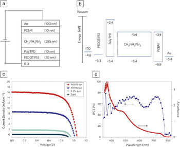
A similar but inverted device concept (the conductive substrate is the hole-extraction contact), where a dual-source evaporated CH3NH3PbI3 perovskite film was sandwiched between organic charge-transport layers ( Figure 3 a), has also been demonstrated. Reference Malinkiewicz, Yella, Lee, Espallargas, Graetzel, Nazeeruddin and Bolink11 The organic semiconductors were chosen to match the conduction and valence bands of the perovskite absorber (Figure 3b). In this case, a thin layer (10 nm) of poly(N,N′-bis(4-butylphenyl)-N,N′-bis(phenyl)benzidine) (polyTPD) was used as the HTL acting, due to its low electron affinity, also as an electron-blocking layer. In between the transparent electrode and the polyTPD, a thin layer of poly(3,4-ethylenedioxythiophene) poly(styrene sulfonate) (PEDOT:PSS) was used as the hole-injection layer (HIL). On the other contact, a 10-nm-thick [6,6]-phenyl C61-butyric acid methyl ester (PCBM) layer ensured selective extraction of the photogenerated electrons. Such simple devices reached efficiencies of 12%, with high open-circuit voltage and fill factor (FF) (Figure 3c–d). Reference Malinkiewicz, Yella, Lee, Espallargas, Graetzel, Nazeeruddin and Bolink11 Further optimization of this same device architecture, in particular by fine tuning the perovskite layer thickness and the electron injection interface, resulted in solar cells with efficiencies as high as 15%. Reference Malinkiewicz, Roldán-Carmona, Soriano, Bandiello, Camacho, Nazeeruddin and Bolink6
(a) Structure of a solar cell employing organic charge-transport layers, (b) schematic of the corresponding flat band energy level diagram, and (c) J–V characteristics of a perovskite solar cell recorded at different irradiance and in the dark. Independent of the light intensity, the device exhibited very similar efficiencies. The high open-circuit potential indicates that there are negligible surface and sub-bandgap states in the perovskite film. (d) Optical absorption (red) and incident photon to current conversion efficiency (IPCE) spectra (blue) obtained for the same device structure. The steep onset in the IPCE spectra corresponds to the band-to-band perovskite absorption. Adapted with permission from Reference 11. Note: ITO, indium tin oxide; PCBM, [6,6]-phenyl C61-butyric acid methyl ester; PEDOT:PSS, poly(ethylenedioxythiophene) poly(styrene sulfonate); polyTPD, poly(N,N′-bis(4-butylphenyl)-N,N′-bis(phenyl)benzidine).

This configuration is particularly advantageous since ETL/HTL can be independently varied, selecting the desired materials from the large library of commercially available organic semiconductors. Lin et al. demonstrated this by studying a series of different hole-transport materials in this simple device configuration. Reference Lin, Armin, Nagiri, Burn and Meredith10 Optimum performance was found when the hole-transporting polymer PCDTBT (poly(N-9′-heptadecanyl-2,7-carbazole-alt-5,5-(4′,7′-di(thien-2-yl)-2′,1′,3′-benzothia- diazole))), with an ionization potential of 5.3 eV, was used. Polander et al. took a similar approach by studying the effect of a series of hole-transporting molecules, using again an “inverted” device configuration. Reference Polander, Pahner, Schwarze, Saalfrank, Koerner and Leo39 The HTL was a double layer consisting of a partially oxidized (doped) layer and an intrinsic layer. A series of organic semiconductors with ionization potentials ranging from 5.0 to 5.6 eV were investigated. The devices employing materials with ionization potentials of up to 5.3 eV yielded improved V oc, while, beyond this range, the absence of a driving force for hole extraction led to a decrease in both J sc and V oc . Reference Polander, Pahner, Schwarze, Saalfrank, Koerner and Leo39 Kim et al. used double-layer hole- and electron-transport contacts with improved energy level alignment. Reference Kim, Kim, Choi, Shim and Kim40 They obtained very high V oc (1.12 V) by employing a MoO3/NPB (NPB: N,N′-Di(1-naphthyl)-N,N′-diphenyl-(1,1′-biphenyl)-4,4′-diamine) HTL and a C60/BCP (BCP: bathocuproine) ETL. These fully vacuum-deposited devices showed PCEs up to 13.7%, with remarkable cell-to-cell reproducibility.
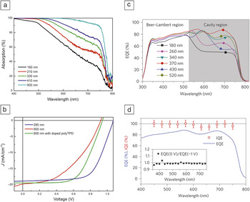
One of the advantages of dual-source vapor deposition is the possibility of preparing highly crystalline perovskite films of arbitrary thickness. Momblona et al. prepared inverted solar cells, with the layout PEDOT:PSS/polyTPD/CH3NH3PbI3/PCBM/Au, employing perovskite layer thicknesses ranging from 200 to 900 nm. Reference Momblona, Malinkiewicz, Roldán-Carmona, Soriano, Gil-Escrig, Bandiello, Scheepers, Edri and Bolink41 By increasing layer thickness, most of the incident light with energy above the CH3NH3PbI3 bandgap is absorbed ( Figure 4 a). J sc increased with increasing perovskite layer thickness, first quickly up to 300 nm and then more slowly for devices with thicker active layers. However, due to a decreasing FF, PCE is reduced for the thicker devices. Partial oxidation of the HTL in cells with a 900 nm perovskite layer led to recovery of the FF and efficiency (Figure 4b). Reference Momblona, Malinkiewicz, Roldán-Carmona, Soriano, Gil-Escrig, Bandiello, Scheepers, Edri and Bolink41 This shows that with non-limiting organic layers, cell performance is independent of perovskite thickness and demonstrates very large charge diffusion length for electrons and holes in these materials.
(a) Absorption spectra for perovskite films with increasing thickness. (b) Photocurrent density (J) versus voltage under 1 sun illumination for a device using non-doped hole-transport layers with a thin (285 nm) and a thick (900 nm) perovskite layer and for a device with a 900-nm-thick perovskite layer but employing a doped hole-transport layer. One advantage of vacuum deposition is the layer absorption (thickness) can be arbitrarily controlled. For thick perovskite layers, however, the conductivity of the charge-transport layers must be adjusted to account for the larger carrier density. Reprinted with permission from Reference 41. © 2014 AIP Publishing. (c) External quantum efficiency (EQE) spectra of devices with different perovskite layer thicknesses. In the cavity region, where the perovskite has lower absorption, interference causes the EQE to be highly thickness-dependent. (d) EQE and internal quantum efficiency (IQE) spectra of a CH3NH3PbI3 device. The IQE is spectrally flat and close to 100% within the error of measurement (±5%). The inset shows the ratio of EQE measured without bias and with a −1 V reverse bias showing that carrier extraction is essentially lossless. Reproduced with permission from Reference 10. © 2015 Nature Publishing Group. Note: polyTPD, poly(N,N′-bis(4-butylphenyl)-N,N′-bis(phenyl)benzidine).

In hybrid perovskite devices, the optimum photoactive layer thickness has been experimentally found to lie between 300 and 400 nm. Lin et al. accurately measured the refractive index (n) and extinction coefficient (k) for a CH3NH3PbI3 layer and hence were able to model the optical-field distribution in a complete device. Reference Lin, Armin, Nagiri, Burn and Meredith10 They predicted two different regimes of behavior: (1) for wavelength λ < 500 nm, no optical field reaches the back electrode as a result of the high-absorption coefficient of the perovskite; (2) for λ > 500 nm, the perovskite is weakly absorbing, and the optical field is dominated by the cavity interference. They consolidated the model by measuring the external quantum efficiency (EQE) of solar cells as a function of the CH3NH3PbI3 layer thickness (Figure 4c). For λ < 500 nm, there is minimal influence of the film thickness, due to the almost complete light absorption by the perovskite cell, while for λ > 500 nm, the EQE is strongly thickness dependent, as predicted by the cavity modeling. By using organic charge-transport layers and a 370-nm-thick perovskite film, record vapor-deposited solar cells, with a PCE of 16.5%, were demonstrated. Reference Lin, Armin, Nagiri, Burn and Meredith10 Interestingly, the correspondent internal quantum efficiency (IQE) is spectrally flat and close to 100% between 450 nm and 750 nm (Figure 4d), confirming the near-unity charge generation and collection efficiency of these perovskite solar cells.
An intrinsic feature of dual-source vapor deposition is the low-temperature processing of the perovskite, especially in the case of using stoichiometric conditions where no post annealing is needed. Reference Malinkiewicz, Yella, Lee, Espallargas, Graetzel, Nazeeruddin and Bolink11 Roldán-Carmona et al. demonstrated flexible perovskite solar cells with a PCE of 7% by employing a 50-μm-thick polyethylene terephthalate (PET) foil coated with a transparent electrode as the substrate. Reference Roldán-Carmona, Malinkiewicz, Soriano, Mínguez Espallargas, Garcia, Reinecke, Kroyer, Dar, Nazeeruddin and Bolink42 The electrode consisted of AZO (30 nm)/Ag (9 nm)/AZO (30 nm), where AZO is Al-doped ZnO at 2 wt% Al. Solar cells were built using a 260-nm-thick CH3NH3PbI3 active layer sandwiched in between organic transport layers. Since the hybrid perovskite is a polycrystalline material, cracks or other imperfections may occur upon bending it. The authors studied the effect of repeated bending of the solar cells and apart from a slight initial decrease of the FF, did not observe any reduction in key performance indicators. Notably, the PCE decreased only about 0.1%, indicating that, despite their polycrystalline nature, hybrid perovskites have the potential of being applied in future flexible electronics applications.
Sequential vacuum deposition
As described previously, sequential vacuum deposition is being increasingly adopted as an alternative effective method for obtaining highly crystalline hybrid perovskites. Several variations of this process have been reported so far. Liu et al. used the thermal evaporation of PbI2 films with subsequent dipping in MAI solutions as a reproducible method for preparing perovskite thin films with precise control over final film thickness. Reference Liu, Gangishetty and Kelly18 At the optimum thickness of 330 nm, ITO/ZnO/CH3NH3PbI3/P3HT/Ag devices were found to have PCEs of up to 11.3%, which is remarkable for devices using poly(3-hexylthiophene) (P3HT) as the HTL. A similar modified process, where the MAI is deposited by hybrid CVD, also demonstrated devices with PCE as high as 11.8%. Reference Leyden, Ono, Raga, Kato, Wang and Qi19
Further variation of this method is the full-vacuum sequential sublimation of the inorganic and organic precursor. Reference Chen, Kang, Hsiao, Yang, Chiang and Lin7,Reference Hu, Wang, Zhou, Zhang, Lv, Pang, Chen, Liu, Padture and Cui20 In this case, the sublimed PbCl2 converted to perovskite in situ upon MAI deposition, resulting in uniform thin films with large-scale homogeneous crystalline structures at an optimized substrate temperature. The corresponding solar cells, employing an organic double ETL (C60/bathophenanthroline), did not make use of an HTL but relied solely on a thin PEDOT:PSS HIL. This is possible due to the ambipolar character of CH3NH3PbI3−x Cl x and the presence of a high built-in voltage in the device, resulting in efficient carrier extraction even without selective contacts. Reference Mei, Li, Liu, Ku, Liu, Rong, Xu, Hu, Chen, Yang, Grätzel and Han43,Reference Laban and Etgar44 The HTL free configuration delivered remarkable performance, with J sc = 20.89 mA/cm–2, FF = 72.2%, and PCE as high as 15.4%.
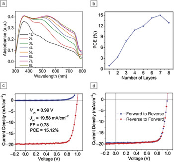
In a similar fashion, perovskite can be obtained through sequential deposition of alternating thin PbX2/MAI multilayers, where the MAI reaction can take place in solution Reference Sutherland, Hoogland, Adachi, Kanjanaboos, Wong, McDowell, Xu, Voznyy, Ning, Houtepen and Sargent22 or in the vapor phase. Reference Chen, Chen and Dai8 This strategy allows for precise control over the thickness and thus optical absorption of the CH3NH3PbI3−x Cl x films ( Figure 5 a). PCE of solar cells with structure ITO/PEDOT:PSS/CH3NH3PbI3−x Cl x /PCBM/Ca-Al shows an almost linear dependence on the number of deposited PbCl2/MAI layers (Figure 5b), suggesting highly uniform growth of well-defined crystalline films. For seven deposition cycles, the PCE exceeded 15% with high FF and J sc, and the J–V characteristics are essentially free of hysteresis (Figure 5c–d), which points again to a well-crystalized, defect-free active layer.
(a) Optical absorbance spectra of layer-by-layer growth CH3NH3PbI3−x Cl x perovskite films with different number of layers, and (b) corresponding solar-cell power-conversion efficiency (PCE). (c) J–V characteristics under illumination (red) and in the dark (blue) for a layer-by-layer perovskite device with corresponding (d) forward and reverse bias scan. Adapted with permission from Reference 8. Note: V oc, open-circuit voltage; J sc, short-circuit current density; FF, fill factor.

Conclusion
Vacuum deposition methods are powerful tools for obtaining flat, homogeneous, and crystalline hybrid perovskite thin films, showing optical and electronic properties analogous to those used in high-efficiency solution-processed perovskite solar cells, with the advantage of process compatibility with any type of substrate due to the low temperatures used. Moreover, perovskite photovoltaics are potential candidates for complementing Si or copper indium gallium selenide cells in monolithic tandem devices, consisting of multilayer stacks of several different materials. From this perspective, vacuum deposition methods offer a unique opportunity, allowing the deposition of perovskite thin films of arbitrary thickness on any type of material (without issues of re-dissolution or intermixing with the bottom layer).
Acknowledgments
We acknowledge support from the Spanish Ministry of Economy and Competitiveness (MINECO) (MAT2014–55200) and the Generalitat Valenciana (Prometeo/2012/053). C.M. would like to thank the MINECO for a predoctoral contract for a doctoral training grant (previously FPI).