I. INTRODUCTION
Nanoscale manufacturing techniques are essential to live up to the promises made on the prospects of nanotechnology; without methods to rapidly fabricate and test new concepts, innovation in this emerging field can be stifled. Additive manufacturing is already used at the macroscale for rapid prototyping and low volume production in areas such as dental and medical care, automotive, aerospace, fashion, and entertainment. Reference Feenstra, Schaefer, Jay and Scudamore1 These areas have benefited from the freedom of design and reduced time-to-market provided by additive manufacturing. Unfortunately, such rapid prototyping techniques are yet to be developed for nanomanufacturing. Such a technology would have the potential to transform manufacturing on the nanoscale as well. Within the scientific community, the focus has been on tissue engineering, Reference Boland, Ovsianikov, Chickov, Doraiswamy, Narayan, Yeong, Leong and Chua2,Reference Zein, Hutmacher, Tan and Teoh3 electronics, Reference Arias, MacKenzie, McCulloch, Rivnay and Salleo4,Reference Zhang, Zhao, Stoller, Zhu, Ji, Murali, Wu, Perales, Clevenger and Ruoff5 microfluidics, Reference Duffy, McDonald, Schueller and Whitesides6,Reference Unger, Chou, Thorsen, Scherer and Quake7 orthopedics, Reference van Noort8,Reference Ryan, Pandit and Apatsidis9 health care, Reference Giannatsis and Dedoussis10,Reference Narayan, Doraiswamy, Chrisey and Chichkov11 and materials, Reference Gu, Meiners, Wissenbach and Poprawe12 but as the resolution improves more applications such as photovoltaics, Reference Jang, Tambunan, Tak, Nguyen, Kang and Byun13,Reference Krebs14 optics, Reference Mark, Gibbs, Lee and Fischer15 and nanoelectronics Reference Park, Hardy, Kang, Barton, Adair, Mukhopadhyay, Lee, Strano, Alleyne, Georgiadis, Ferreira and Rogers16,Reference Min, Kim, Kim, Cho, Noh, Yang, Cho and Lee17 are emerging.
For decades, realistic options for full scale industrial nanomanufacturing have relied on photolithography using electromagnetic radiation with increasingly shorter wave length. Reference Wagner and Harned18 The equipment to reach nanometer dimensions reliably is, however, prohibitively expensive, thereby excluding smaller R&D facilities and small and medium enterprises (SMEs) from taking advantage of their innovations. Electron beam lithography (EBL) offers flexibility and high resolution Reference Manfrinato, Zhang, Su, Duan, Hobbs, Stach and Berggren19 for R&D and is comparably cheap but is still only affordable for well-funded universities and companies with large capital investments. Device fabrication using both photolithography and EBL relies on exposures of multiple layers of polymer thin films. These are planar technologies operating virtually only in two dimensions; developing fabrication methods that extend into the third dimension seems an obvious way to save space, cost and to gain additional functionality. Moreover, the lift-off and etching processes related to resist-based manufacturing are extremely wasteful as only a small percentage of the used materials is turned into functional elements. Reference Williams, Ayres and Heller20 Additive nanomanufacturing (ANM) does not seek to replace the resist-based planar manufacturing methods used for integrated circuit (IC) fabrication, but rather seeks to add functionally in ways these technologies cannot. More importantly, it could change the way we think about manufacturing at the nanoscale, which could also lead to much greater flexibility in the design.
Before we begin a technical review, we will define ANM as we perceive it for the purposes of this review. We define ANM as incorporating techniques that directly add the desired material in its final shape, with sub-100 nm resolution, without subtractive removal. This definition excludes thin film fabrication methods such as atomic layer deposition (ALD) and molecular beam epitaxy (MBE) although these methods might successfully be combined with additive manufacturing methods. Direct laser writing (DLW), near-field optical lithography, and plasmonic lensing are borderline ANM technologies, as these can produce structures in their final shape after an additional development process. For completeness these are included in the review.
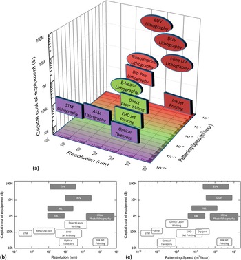
The cost of nanolithography tools is growing rapidly with equipment cost ranging from $1 million to $100 million for the latest extreme UV (EUV) lithography tools. In Fig. 1(a), the patterning speed, resolution, and estimated capital equipment cost of ANM methods (square) are compared to traditional resist-based thin film manufacturing methods (ellipse). The capital equipment cost for ANM methods is generally much smaller than for resist-based manufacturing methods without sacrificing resolution as clarified in Fig. 1(b). This is one of the primary reasons ANM is envisioned to spread to SMEs and research labs. The price per unit can still be high for additive manufacturing Reference Feenstra, Schaefer, Jay and Scudamore1 because of the relatively low patterning speed as shown in Fig. 1(c); but for low volume and high value products, the comparatively low investment prospects of this technique can be particularly attractive.
(a) Equipment cost, patterning speed, and minimum resolution of additive manufacturing methods (square) compared with traditional resist-based lithography methods (ellipse). (b) Projection of the 3D graph in (a) showing the capital cost of equipment versus minimum resolution for ANM methods (white) and traditional resist-based methods (gray). (c) Projection of the 3D graph in (a) showing the capital cost of equipment versus patterning speed for ANM methods (white) and traditional resist-based methods (gray). (EUV = extreme UV lithography, DUV = deep UV lithography, EBL = electron-beam lithography, NIL = nanoimprint lithography, STM = scanning tunneling microscopy, AFM = atomic force microscopy).

When comparing manufacturing methods at the micro- and nanoscale, one often focuses on the resolution of the technology as it is closely linked to the performance of the product. For commercial use, resolution is, however, only one significant parameter as the ability to position structures relative to one another (accuracy/alignment), writing speed and materials are equally important.
Manufacturing at the nanoscale is very different from macroscale manufacturing because of fundamental physical limits. Therefore, the difficulties met are also very different. Fabrication at the nanoscale is a matter of manipulating very few atoms or molecules at a time and manufacturing variations of just a single atom or molecule can lead to device failure. Additionally, structures with dimensions below 50 nm also have a reduced melting point which can affect their mechanical stability Reference Couchman and Jesser21,Reference Allen, Bayles, Gile and Jesser22 and even defining alloy composition, doping levels and crystallinity becomes complex as the presence or spatial location of a single atom will change the material properties. At the nanoscale, gravity is insignificant and the dominating forces are the surface interactions such as van der Waals forces that can cause unwanted adhesion. In liquid, Brownian motion and convection forces are comparatively strong making particle capture difficult. Even in air or vacuum, vibrations from fans, pumps or passing traffic can render structural alignment impossible.
For ANM, the challenge is to manufacture nanoscale structures at a large scale with great accuracy, high resolution, low cost and using materials ranging from biomaterials to ceramics and metals. However, ANM does not aim to compete with existing technologies and it can create new ways to manufacture and change the way we design products. In this review, we focus on the range of ANM methods available today and the level they are at in terms of resolution, accuracy, speed, and materials. We have divided the manufacturing methods into two groups: direct writing and single particle placement. Within each group, the state-of-the-art ANM techniques will be described and evaluated and finally these techniques will be compared to provide an outlook on ANM and its prospects over the next decade.
II. DIRECT WRITING
Direct writing of nanoscale devices composed of metals, insulators, and organic materials is of interest for a range of ANM applications. Here, we review recent advances in three key direct writing methods of nanostructures: dip-pen nanolithography (DPN), electrohydrodynamic (EHD) jet printing, and DLW. All three technologies are able to achieve sub-30 nm resolution, relatively high writing speed, and the capacity for 3-dimensional nanomanufacturing. The choice of materials, at least for DPN and EHD jet printing, is already vast ranging from metals to biomaterials while the material selection for DLW is also increasing. In this section, the promising future of direct writing ANM is outlined through examples of the state-of-the-art for each of these three technologies.
A. Dip-pen nanolithography
DPN is a scanning probe microscopy (SPM)-based flexible nanofabrication process for making 2D nanoscale features that uniquely combines direct-write soft-matter compatibility with the high resolution and registry of atomic force microscopy (AFM), all in a mask-free and biocompatible system. Reference Ginger, Zhang and Mirkin23 Originally, scanning probe microscopes (SPMs), such as the scanning tunneling microscope (STM) Reference Binnig, Rohrer, Gerber and Weibel24 and the atomic force microscope (AFM), Reference Binnig, Quate and Gerber25 emerged as nanoscale imaging and spectroscopic tools in the mid 1980s. Soon thereafter manipulation of single-atoms Reference Gimzewski and Joachim26 and atom-by-atom construction of nanopatterns marked the birth of scanning probe lithography (SPL), suggesting that SPMs could indeed be used for molecular printing or perhaps even manufacturing. Reference Eigler and Schweizer27
Hereafter, a series of indirect SPL methods based on destructive delivery of energy to create functional patterns were developed. Taking advantage of the positioning resolution enabled by piezo-actuation and the nanoscale radii of the tips, scientists were able to generate sub-50-nm features by scratching, etching, and oxidizing surfaces. Reference Xia and Whitesides28 A process known as nanoshaving or nanografting uses the tip of an AFM and an applied force to remove a molecular monolayer on gold in a site-specific fashion Reference Liu, Cruchon-Dupeyrat, Garno, Frommer and Liu29 and anodic oxidation of silicon was developed by Quate and colleagues for patterning silicon substrates. Reference Minne, Manalis, Atalar and Quate30,Reference Minne, Adams, Yaralioglu, Manalis, Atalar and Quate31
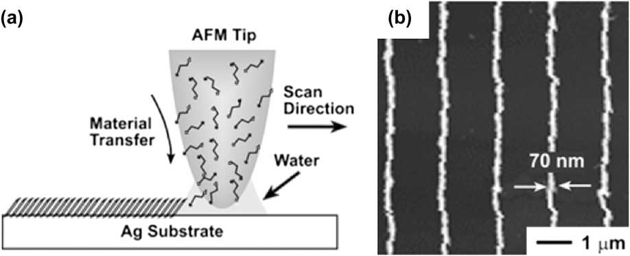
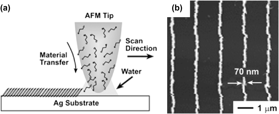
In contrast to nanoshaving and nanografting, DPN selectively transfers material from an ink-coated probe tip on to a surface with a variety of ink-surface combinations. Reference Ginger, Zhang and Mirkin23,Reference Salaita, Wang and Mirkin32 A schematic of the process is shown in Fig. 2. Ink molecules are transported via mass diffusion from the tip on to the surface. Features are formed on the surface via either chemisorption based self-assembly or physisorption. Reference Brown, Eichelsdoerfer, Liao, He and Mirkin35 Ink transport is mediated by the presence of the water meniscus that forms when the tip is brought in close proximity to the surface under ambient conditions. Due to the naturally occurring water meniscus for mass transfer this method also avoids the necessity for ultrahigh vacuum. Moreover, there is no need to expose the substrate to ultraviolet, ion- or electron-beam radiation, characteristic of indirect patterning techniques, and therefore DPN can be used to print fragile or reactive organic and biological materials.
(a) Schematic representation of the basic molecular deposition by DPN through a water meniscus formed between the scanning probe tip and the substrate surface. (b) Direct deposition of SAMs (16-mercaptohexadecanoic acid) on Ag as an etch resist to pattern 70-nm wide features. Reproduced from Refs. Reference Gates, Xu, Stewart, Ryan, Willson and Whitesides33 and Reference Zhang and Mirkin34.
From initial demonstrations involving alkanethiols on gold, Reference Piner, Zhu, Xu, Hong and Mirkin36 DPN has evolved into a versatile technique used to write or template both inorganic and organic nanostructures. Reference Ginger, Zhang and Mirkin23,Reference Salaita, Wang and Mirkin32 Polymers, Reference Nyamjav and Ivanisevic37 colloidal nanoparticles (e.g., magnetic nanocrystals and carbon nanotubes (CNTs)), Reference Suriano, Biella, Cesura, Levi and Turri38–Reference Wang, Maspoch, Zou, Schatz, Smalley and Mirkin40 electrodeposited metals, Reference Li, Maynor and Liu41 sol-gel precursors, Reference Fu, Liu, Zhang, Dravid and Mirkin42 small organic molecules, Reference Lenhert, Sun, Wang, Fuchs and Mirkin43,Reference Hirtz, Antonios, Thanasis, Harald and Aravind44 biomolecules (proteins Reference Lee, Park, Mirkin, Smith and Mrksich45,Reference Lee, Lim and Mirkin46 and oligonucleotides Reference Demers, Ginger, Park, Li, Chung and Mirkin47 ) and even single viruses Reference Vega, Shen, Maspoch, Robach, Lamb and Mirkin48 and bacteria have been patterned on a variety of substrates (including metals, semiconductors, and insulators) Reference Suriano, Biella, Cesura, Levi and Turri38 by controlling various experimental parameters such as ambient humidity, writing speed, and dwell time. Reference Hirtz, Antonios, Thanasis, Harald and Aravind44,Reference Cronin, Sabolsky, Sabolsky and Sierros49 In fact, these experimental parameters serve a useful function of being the levers that control the features size. However, DPN initially faced a drawback common to other indirect SPL of poor throughput. This was because the first incarnations of DPN were serial processes, and were thus lower in throughput than stamping or optical lithography-based techniques. To compete with these techniques, it was necessary to increase the throughput of DPN by parallelizing the deposition process. The scalability of DPN was demonstrated by Salaita et al. Reference Salaita, Wang, Fragala, Vega, Liu and Mirkin50 who were able to fabricate a 55,000-pen 2D array generating 88 million Au dots (pitch distance 400 nm) with a diameter equal to 100 ± 20 nm (see Fig. 3). This increased the throughput of DPN by four orders of magnitude, fabricating the 88 million dots in approximately 5 min. Even with impressive recent advances in cantilever array design, such arrays tend to be highly specialized for a given application. They are also mechanically fragile, expensive, and often difficult to implement. It is therefore difficult to imagine commercially viable production methods based on scanning probe systems that rely on conventional cantilevers. Reference Shim, Braunschweig, Liao, Chai, Lim, Zheng and Mirkin51 Hence new methods to reduce the cost barriers associated with massively parallel DPN were demonstrated to achieve high-throughput and to define patterns with high-resolution. Reference Giam and Mirkin52
(a) Optical micrograph of part of the 2D array of cantilevers used for patterning. Inset: SEM image of the cantilever arrays at a different viewing angle. (b) Large-area SEM image of part of an 88,000,000-gold-dot array (40 × 40 within each block) on an oxidized silicon substrate. (c) Representative AFM topographical image of part of one of the blocks, where the dot-to-dot distance is 400 nm and the dot diameter is 100 ± 20 nm. Reproduced from Ref. Reference Salaita, Wang, Fragala, Vega, Liu and Mirkin50.

The second key advance in molecular printing was therefore to replace the cantilever with an elastomeric pyramid on a solid backing. This approach is called polymer pen lithography (PPL) and is shown in Fig. 4. Reference Huo, Zheng, Zheng, Giam, Zhang and Mirkin53 The elastomeric tips can print a digitized pattern with spot sizes ranging from 90 nm to over 10 μm, simply by changing the force and time over which the ink is delivered. This feature-size dependence on force is a remarkably controllable parameter and distinguishes PPL from both DPN and conventional contact printing. Because the elastomeric tip array can absorb ink and act as a reservoir, it can be used to print over large areas and for multiple printing tasks without re-inking. The patterning capabilities have been demonstrated with arrays that contain anywhere between 15,000 to ∼11,000,000 pyramid-shaped pens. PPL has also proven to be effective for patterning small molecules and proteins and has been used to make patterns of electronic circuits. Reference Huo, Zheng, Zheng, Giam, Zhang and Mirkin53
(a) A schematic illustration of the PPL setup. (b) A photograph of an 11-million-pen array. (c) Scanning electron microscope image of the polymer pen array. The average tip radius of curvature is 70 ± 10 nm (inset). Reproduced from Ref. Reference Huo, Zheng, Zheng, Giam, Zhang and Mirkin53.

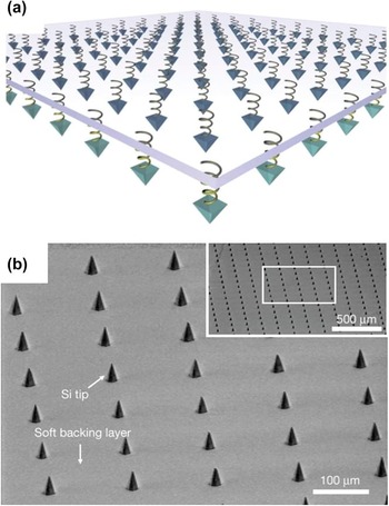
A third key advance was to overcome the feature size limits of elastomeric pens in PPL by fabricating arrays of ultra-sharp Si tips on a spring-like elastomer layer that allows all of the tips to be brought into contact with a surface over large areas. This method is called hard-tip, soft-spring lithography Reference Shim, Braunschweig, Liao, Chai, Lim, Zheng and Mirkin51 (HSL) and is illustrated in Fig. 5. In HSL, there is a lack of feature diameter dependence on the force exerted between the tip array and the surface, because Si tips do not deform under pressure. However, there is a linear relationship between the feature area and the square root of the dwell time. HSL is also distinguished from all other lithographic techniques by the ability to form arbitrary patterns in massively parallel (over a 1-cm2 area) and mask-less fashion at a feature resolution of less than 50 nm.
(a) Schematic illustration of a HSL tip array supported by a transparent, soft backing layer that provides mechanical flexibility to each tip. (b) An SEM image of the Si tip array on SiO2/PDMS/glass with a 150-μm pitch between tips. The inset shows a large area of the array to demonstrate the homogeneity of the tips. Reproduced from Ref. Reference Shim, Braunschweig, Liao, Chai, Lim, Zheng and Mirkin51.

Other challenges such as the direct writing of single sub-10 nm nanoparticles in a specific location individually on a substrate have allowed further development of DPN. Scanning probe block co-polymer lithography (SPBCL) Reference Chai, Huo, Zheng, Giam, Shim and Mirkin54 relies on either DPN or PPL to transfer phase-separating block copolymer inks in the form of 100 nm or larger features on an underlying substrate. Reduction of the metal ions via plasma results in the high-yield formation of single crystal nanoparticles per block copolymer feature. For instance, integration of individual nanoparticles on devices Reference Liu, Eichelsdoerfer, Rasin, Zhou, Brown, Liao and Mirkin55 or single-molecule protein arrays Reference Chai, Wong, Giam and Mirkin56 has been enabled by scanning probe block copolymer lithography.
More recently, a cantilever-free SPL architecture that can generate 100 nm-scale molecular features using a 2D array of independently actuated probes has been reported. Reference Brown, Eichelsdoerfer, Shim, Rasin, Radha, Liao, Schmucker, Liu and Mirkin57 To physically actuate a probe, local heating is used to thermally expand the elastomeric film beneath a single probe, bringing it into contact with the patterning surface. Not only is this architecture simple and scalable, but it addresses fundamental limitations of 2D SPL by allowing one to compensate for unavoidable imperfections in the system. This cantilever-free dot-matrix nanoprinting will enable the construction of surfaces with chemical functionality that is tuned across the nano- and macroscales.
In the latest DPN development called beam pen lithography, an array of tips adds photosensitive material to the surface followed by exposure of the material through a hole in the tip. Reference Bian, Zieba, Morris, Han, Richter, Brown, Mirkin and Braunschweig58 Although nanoscale features have not yet been achieved, one could envisage combining this method with near-field photolithography to create nanoscale three-dimensional (3D) structures.
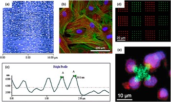
DPN has been widely applied to deposit biological material on a subcellular scale. The absence of high temperatures and aggressive chemicals makes DPN an excellent tool for sensitive biological materials such as proteins, peptides, DNA, lipids, viruses, and enzymes. As an example Curran et al. Reference Curran, Chen, Stokes, Irvine, Graham, Gubbins, Delaney, Amro, Sanedrin, Jamil and Hunt59 reported DPN deposition for subcellular surface modification in stem cell growth by depositing arrays of 70 nm dots with varying pitch [see Figs. 6(a)–6(c)]. The dots contained self-assembled monolayers (SAMs) with –OH, –CH3, –CO2H, or –NH2 termination to control the initial stem cell attachment and subsequent cell signaling. In this case, DPN provided a method to rapidly scan for stem cell growth factors by large-area nanoscale surface-modification, which is difficult to achieve by other fabrication technologies. Sekula et al. Reference Sekula, Fuchs, Weg-Remers, Nagel, Schuppler, Fragala, Theilacker, Franueb, Wingren, Ellmark, Borrebaeck, Mirkin, Fuchs and Lenhert60 showed that DPN can be used to deposit phospholipids containing various amounts of biotin and/or nitrilotriacetic acid functional groups with a 200 nm resolution. The structures were selectively functionalized and subsequently used for selective adhesion and activation of T-cells [see Figs. 6(d) and 6(e)]. One benefit of using ANM is the ability to add functionality to existing structures. This was shown by Mitsakakis et al. Reference Mitsakakis, Sekula-Neuner, Lenhert, Fuchs and Gizeli61 by using DPN to deposit lipids with different functionalized head groups on a microfluidic surface acoustic wave biosensor. By using DPN, the sample preparation time was reduced and the sensitivity of the biosensor was increased 5 times. It is beyond the scope of this article to give an exhaustive review of all the biomaterials deposited by DPN but an overview can be found in two excellent reviews by Zhou et al. Reference Zhou, Boey, Huo, Huang and Zhang62 and Wu et al. Reference Wu, Reinhoudt, Otto, Subramaniam and Velders63
(a) AFM image of SAM dots printed using DPN. (b) Human stem cells grown on nanopatterned surface. (c) Height profile of nanodots of SAMs. (d) Fluorescence micrograph of phospholipid nanodots patterned by DPN. (e) Fluorescence micrograph of a T-cell selectively adhered to and activated by functional proteins (anti-CD3/anti-CD28 antibodies) bound to phospholipid multilayer patterns via streptavidin. (a)–(c) reproduced from Ref. Reference Curran, Chen, Stokes, Irvine, Graham, Gubbins, Delaney, Amro, Sanedrin, Jamil and Hunt59. (d), (e) reproduced from Ref. Reference Sekula, Fuchs, Weg-Remers, Nagel, Schuppler, Fragala, Theilacker, Franueb, Wingren, Ellmark, Borrebaeck, Mirkin, Fuchs and Lenhert60.

DPN has evolved to achieve unlimited pattern design, low-cost, high throughput, and pattern flexibility. The advances have been rapid and span many fields. However, issues such as individual tip actuation over large areas, feature size reduction to the single-molecule level (for example, individual proteins), and translation of the tips over large distances must be addressed to achieve the full potential of this technology. The use of these techniques as tools for rapid and parallel site-specific chemical transformations is an emerging approach that could transform the manufacturing of gene chips by providing a route to site-specific combinatorial synthesis. Rapid advances in tip engineering to reduce wear have been particularly important. Reference Bhaskaran, Gotsmann, Sebastian, Drechsler, Lantz, Despont, Jaroenapibal, Carpick, Chen and Sridharan64–Reference Fletcher, Felts, Dai, Jacobs, Zeng, Lee, Sheehan, Carlisle, Carpick and King67
B. Electrohydrodynamic jet printing
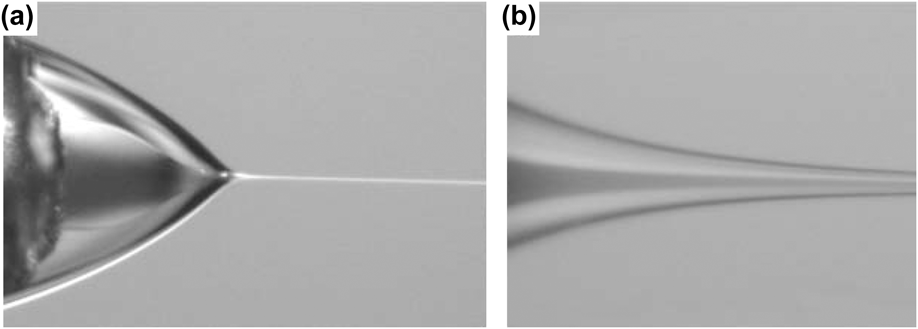
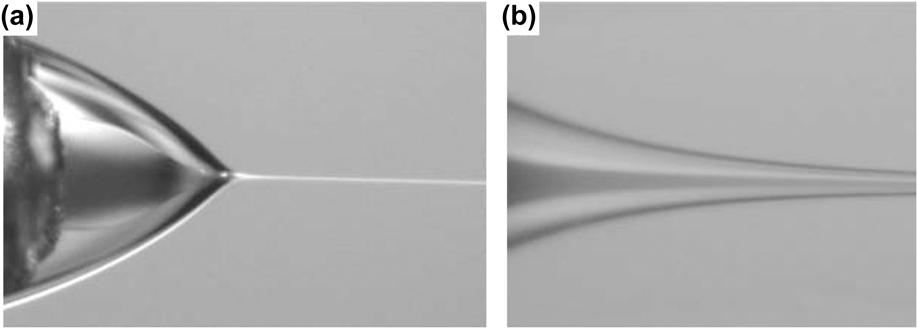
Inkjet printing by piezoelectric actuation is well known from home printing of documents and photos. The same technology with a little modification has been used to print microscale structures of a wide variety of materials including proteins, Reference Delaney, Smith and Schubert68 polymers, Reference Krebs14 and nanoparticles. Reference Fuller, Wilhelm and Jacobson69 An alternative driving force to expel the “ink” known as electrohydrodynamic (EHD) jet printing utilizes an electric potential applied between the nozzle and the substrate. The electric potential causes mobile ions to accumulate near the mouth of the nozzle and due to ionic electrostatic repulsion the meniscus deforms into a cone known as the Taylor cone Reference Park, Hardy, Kang, Barton, Adair, Mukhopadhyay, Lee, Strano, Alleyne, Georgiadis, Ferreira and Rogers16 consisting of one or more coaxial liquids (see Fig. 7). At low electric fields, the meniscus enters a pulsating mode in which the Taylor cone contracts after expelling each droplet. The frequency of this pulsation is in the kilohertz range leading to a rapid stream of droplets before the meniscus retracts to its original shape. The time it takes to form a new burst of droplets depends on the flow rate of the supplied solution and the characteristic charging time determined by the resistance and capacitance of the system. If the electric field is increased, the Taylor cone stabilizes and a continuous flow is established known as the stable jet mode which is used in electrospinning. At even higher electric fields, multiple jets can form and eventually the atomization mode is reached (also known as electrospraying) in which a fine cloud of droplets is created, a method widely used in mass spectroscopy and for thin film deposition. Thus, EHD jet printing can be harnessed to directly write structures in two or three dimensions or apply thin films with great uniformity. The key advantage of EHD jet printing over other dispensing technologies is that by controlling the electric field strength, droplets or liquid streams with a diameter much smaller than the nozzle size can be achieved. Reference Barrero and Loscertales70,Reference Choi, Park, Park, Ferreira, Georgiadis and Rogers71 Nozzle clogging is exacerbated by a reduction in the nozzle orifice and is one of the main causes of dispensing failure. Clogging in addition to the difficulties of nanoscale nozzle fabrication are some of the main challenges in any nanoscale dispensing technology.
(a) Photograph of compound Taylor cone containing coaxial fluid flow. (b) Close-up of coaxial jet. Reproduced from Ref. Reference Barrero and Loscertales70.
Through the pulsating mode, Park et al. Reference Park, Hardy, Kang, Barton, Adair, Mukhopadhyay, Lee, Strano, Alleyne, Georgiadis, Ferreira and Rogers16 were the first to show that EHD jet printing can achieve feature sizes below 250 nm by using nozzles with an internal diameter down to 300 nm and reducing the nozzle to sample distance to 100 µm. By coating the nozzle opening in a hydrophobic SAM clogging and erratic dispensing was avoided enabling high quality printing. Through an integrated computer-controlled system, the group showed printing of complex structures in both conducting and insulating polymers as well as solutions of silicon nanoparticles and rods and single wall CNTs. They were also able to show printing of interconnects and functional transistors with critical dimensions down to 1 µm on a flexible plastic substrate.
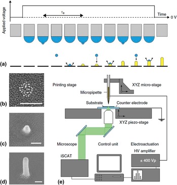
EHD jet printing was taken even further by Galliker et al. Reference Galliker, Schneider, Eghlidi, Kress, Sandoghdar and Poulikakos72 who improved the resolution and extended the technology into the third dimension through electric field enhancement and rapid solvent evaporation. The resolution was improved by reducing the substrate to nozzle distance to 3–4 µm which enabled structures down to 50 nm to be written (see Fig. 8). The electric field enhancement from the first droplet guides the second droplet to land in exactly the same spot. In this way, vertical and tilted gold nanowires with a 50 nm diameter and 850 nm height could be fabricated [see Fig. 8(d)].
Schematic of EHD printing process and setup. (a) Growth of a liquid meniscus and subsequent ejection of ink nanodroplets from its apex on application of a DC voltage. During DC on-time, droplets are ejected at a homogenous period τe and, once impacted, are vaporized (represented by wavy arrows) in the course of τe. After periodic repetition of this event (for illustration convenience merged into one cycle), a sharp structure consisting of a multitude of formerly dispersed nanoparticles rises from the substrate, attracting approaching charged droplets by electrostatic nanodroplet autofocusing (straight arrows). The growth process is further illustrated with SEM micrographs (150 nm scale bar) of (b) the deposition pattern of a single nanodroplet and that of (c, d) actual nanopillars. (e) Schematic of the ENA NanoDrip setup with the nozzle located above an underlying glass substrate placed on an ITO-coated glass slide representing the grounded counter electrode. Voltage stimuli were applied in the form of amplified DC signals between the ink-filled, metal-coated pipette and the counter electrode. Reproduced from Ref. Reference Galliker, Schneider, Eghlidi, Kress, Sandoghdar and Poulikakos72.

The nonlinear relationship between the applied voltage and droplet diameter was shown experimentally to vary the droplet diameter from the size of the nozzle orifice (1.2 µm) down to 80 nm at which point further electric field increments had no effect on the droplet diameter. This 15x reduction in feature size helps preventing clogging and enables microstructures to be written with the same nozzle as nanostructures. The applied voltage also increases the frequency with which the droplets are expelled (up to ≈100 kHz) and thereby the flow rate of the dispensed solvent. The increased frequency was shown to be outweighed by the reduction in droplet diameter thereby reducing the overall flow rate by almost a factor 100. However, near the minimum droplet diameter, the flow rate reaches a minimum and further increase in applied voltage was able to restore the flow rate to near its original value (≈100 µm3/s). The implications of this is that with the given nozzle size, 80 nm wide lines can be written faster than 1 µm wide lines. Such inverse scaling of throughput to feature size is in contrast to other techniques and can thus be advantageous for nanomanufacturing.
Combining EHD jet printing with block-copolymer self-assembly provides a pathway for further reduction in minimum feature size. The flexibility of EHD jet printing allows a desirable mixing of block-copolymers with different molecular weight and the material waste of the relatively expensive polymers is greatly reduced. In this way, periodic structures with length scales ranging from centimeters to ≈10 nm can be fabricated Reference Onses, Song, Williamson, Sutanto, Ferreira, Alleyne, Nealey, Ahn and Rogers73 within the geometrical limitations of block-copolymer self-assembly.
Electrospinning from the stable jet mode is used for fast deposition of organic and polymer fibers for applications in nanowire electronic devices, physical biomimetic structures, and field-effect transistors. Traditional electrospinning can form fibers with speeds up to 10 m/s but the fibers are unaligned and form a mat of cross-linked fibers because of an uncontrollable wiping motion of the forming fiber. Reference Huang, Bu, Duan, Pan, Liu, Yin and Xiong74 By reducing the distance between the nozzle and the substrate, straight fiber arrays can be formed. Reference Sundaray, Subramanian, Natarajan, Xiang, Chang and Fann75,Reference Huang, Wang, Duan, Bu and Yin76 Through a further reduction of the distance and the applied voltage, the fiber diameter can be reduced to 50 nm and positioned with great accuracy. Reference Bisht, Canton, Mirsepassi, Kuinsky, Oh, Dunn-Rankin and Madou77 A further development known as mechano-electrospinning utilizes the drawing force on the fiber from the moving stage to stretch the fiber Reference Bu, Huang, Wang and Yin78 achieving well-organized arrays of sub-20 nm diameter fibers. Reference Bisht, Canton, Mirsepassi, Kuinsky, Oh, Dunn-Rankin and Madou77 The fiber diameter decreases with the drawing speed and could be drawn with up to 40 mm/s. Recently, Lee et al. Reference Lee and Kim79 extended electrospinning to the third dimension by utilizing the electric field enhancement from a Pt electrode to control the wiping motion. By repeatedly passing the fiber along the same path, 180 nm wide and 4.5 µm tall walls of poly(ethylene oxide) were deposited (see Fig. 9). Additional advantages of electrospinning is the ability to fabricate hollow, Reference Li and Xia80 co-axial, Reference Zhang, Wang, Feng, Li, Lim and Ramakrishna81 and mixed composition nanowires Reference Wang, Jayasinghe, Edirisinghe and Luklinska82 in one step. An impressive example of the materials and dimensions achievable by electrospinning was reported by Nuansing et al. Reference Nuansing, Frauchiger, Huth, Rebollo, Hillenbrand and Bittner83 who were able to deposit peptide and protein nanowires with a diameter around 100 nm but on occasion down to 5 nm, corresponding to a single molecule (see Fig. 10). These fibers will be highly biocompatible and biodegradable and a potential candidate for the most critical biological and medical applications, such as the proliferation of stem cells. Although these nanofibers were randomly orientated, the recent advances within EHD jet printing mentioned previously in this review would enable controlled deposition.
Poly(ethylene oxide) 3D structures fabricated by electrospinning. Reproduced from Ref. Reference Lee and Kim79.

(a)–(c) Biocompatible albumin (protein) nanofibers with diameters below 100 nm fabricated by electrospinning. Reproduced from Ref. Reference Nuansing, Frauchiger, Huth, Rebollo, Hillenbrand and Bittner83.

Electrospraying (electrohydrodynamic spraying) is a method closely related to EHD jet printing in that an electric potential is applied between the nozzle and the sample to draw the solution containing charged particles from the nozzle. The distinction of this technique with regards to the pulsating and stable jet mode is that the electric field is much higher in this technique. In electrospraying, the repulsive forces from the charged particles overcome the surface tension of the expelled liquid thereby breaking up the solution into droplets. Potential evaporation of the solution increases the repulsive surface charges thereby further breaking up the droplet into a cloud of micro- or nanodroplets. Reference Salata84 The size of virtually monodisperse droplets can be controlled by the solution flow rate, electrical potential at the nozzle, and nozzle diameter. Because the droplets are electrically charged, coagulation is absent. The trajectory and focus of the charged particle beam can also be controlled by an external electric field. Reference Jaworek and Sobczyk85 In this way, Lee et al. were able to focus electrosprayed silver nanoparticles to write lines 100 µm wide and 100 nm thick with a deposition rate of 2 µL/min. Reference Lee, Shin, Park, Yu and Hwang86
Electrospraying is a flexible deposition method that has been used for thin film deposition, direct writing, and nanoparticle fabrication within a variety of fields. Virtually all materials can be electrosprayed, which means that organic as well as inorganic thin films can be formed. An excellent review paper by Jaworek et al. Reference Jaworek and Sobczyk85 lists more than 40 materials and their solvents that have been used so far. Due to the spraying nature of the process, the resolution of the process is currently limited to 100 µm for direct writing. Therefore, electrospraying is not suited for direct writing of nanostructures but can distribute nanoparticles locally. However, electrospraying is a mature technology with a wide range of proven material choices which for the most can be used for nanofabrication if operating in the pulsating or stable jet mode EHD jet printing. A search for materials to use in EHD jet printing can hereby benefit from looking through the literature for electrospraying.
Taking into account the high writing speeds, wide material choice, and ability to print in three dimensions, the possibilities for EHD jet printing are vast. However, because EHD jet printing does not have an inbuilt alignment technique, as is the case for manufacturing technologies based on microscopy techniques, aligning consecutive layers will prove more difficult. Nevertheless, this technology is one of the most promising ANM technologies for large-scale fabrication of structures where nanoscale alignment is not essential.
C. DLW and resist-based nanomanufacturing
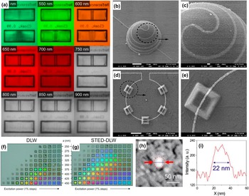
DLW of nanoscale features is capable of building 3D structures from the ground up in a rapid and facile manner (see Fig. 11). Although DLW is a resist-based fabrication method and therefore requires an additional development step, it is very similar in nature to additive nanofabrication because the fabricated structures have their final shape without following deposition or etch steps. Laser driven 3D nanofabrication is best achieved by multiphoton polymerization (MPP). Reference Kawata, Sun, Tanaka and Takada91,Reference Deubel, von Freymann, Wegener, Pereira, Busch and Soukoulis92 In MPP, the concentration of photons in the neck of a femtosecond pulse of a laser beam allows for the controlled photopolymerization of a targeted volume (or voxel) in a photoresist. Development of this resin allows 3D features to be written at typically 10–500 µm/s with nanoscale resolution. This is particularly useful for fabricating 3D photonic structures Reference Fischer, Ergin and Wegener87,Reference Deubel, von Freymann, Wegener, Pereira, Busch and Soukoulis92,Reference Ergin, Stenger, Brenner, Pendry and Wegener93 that would otherwise be extremely expensive and difficult to manufacture with the alignment of sequential 2D layers via traditional lithography. The successful commercialization of this technology by companies like Nanoscribe GmbH has enabled photonics researchers to investigate new applications in 3D with invisibility cloaks, Reference Fischer, Ergin and Wegener87,Reference Ergin, Stenger, Brenner, Pendry and Wegener93 Gecko-mimicking surfaces, Reference Röhrig, Thiel, Worgull and Hölscher94 and 3D data storage Reference Li, Cao and Gu95 among other impressive achievements in recent years.
Features and devices created by DLW literature. (a) True color images of carpet invisibility cloak for unpolarized light, ranging in wave length from 500 to 900 nm, with both reference and cloak structures. Reproduced from Ref. Reference Fischer, Ergin and Wegener87. (b–e) SEM images of silver microscale lines drawn arbitrarily onto 3D structures. Reproduced from Ref. Reference Xu, Xia, Niu, Zhang, Sun, Chen, Xu, Lv, Li, Misawa and Sun88. (f, g) True-color reflection-mode optical micrographs of woodpile photonic crystals 20 × 20 µm2 fabricated by (f) regular DLW (MPP) and (g) STED-DLW. Reproduced from Ref. Reference Fischer and Wegener89. (h) SEM image of a 22 nm silver dot grown by laser driven nucleation and growth, with (i) the corresponding intensity profile as indicated in the micrograph. Reproduced from Ref. Reference Cao and Gu90.

The range of materials that can be polymerized for MPP nanofabrication is a significant challenge for materials science to explore. For solid structures, advanced composites or solutions that respond to MPP have been demonstrated, resulting in structures of vanadium Reference Kabouraki, Giakoumaki, Danilevicius, Gray, Vamvakaki and Farsari96 and silver. Reference Cao and Gu90 The simplest approach to avoid this is to use the surfaces of 3D polymer structures as scaffolds for the deposition of other materials. Metallization of such scaffolds by ALD or electroless plating has been shown to work for metallic photonic crystals Reference Vasilantonakis, Terzaki, Sakellari, Purlys, Gray, Soukoulis, Vamvakaki, Kafesaki and Farsari97 and metamaterials. Reference Staude, Decker, Ventura, Jagadish, Neshev, Gu and Kivshar98 The polymer structures written can also be used for casting of 3D structures from other materials like titania. Reference Frölich, Fischer, Zebrowski, Busch and Wegener99
Maximizing the resolution of MPP is of course an important goal, with Abbe's diffraction limit representing the typical limit. A recent review Reference Fischer and Wegener100 summarized the advances in sub-diffraction limit DLW. As an example Cao et al. achieved the highest resolution of this technique to date with 40 nm dots in a highly sensitive photoresin Reference Cao, Gan, Jia, Evans and Gu101 and 22 nm silver dots by laser activated nanoparticle growth. Reference Cao and Gu90 These results are extremely impressive, but the high resolution was only achievable for individual dots. When continuous structures were attempted, a larger line width of 130 nm was achieved at a comparatively low scanning speed of 3 µm/s. Reference Cao, Gan, Jia, Evans and Gu101 Stimulated emission depletion (STED), which has achieved 5.8 ± 0.8 nm resolution in microscopy, Reference Rittweger, Han, Irvine, Eggeling and Hell102 is also being put forward as a promising route to sub-diffraction MPP. It has been effective in building 3D nanoscale structures over a large area Reference Fischer, Ergin and Wegener87,Reference Frölich, Fischer, Zebrowski, Busch and Wegener99 and shows significant improvement over regular MPP for 175 nm parallel structures Reference Fischer and Wegener89 achieving 65 nm line widths Reference Fischer, von Freymann and Wegener103 whilst scanning at 100 µm/s.
DLW is also able to create a wider range of features in 2D by initiating reactions locally with the input of energy from the laser. This includes reducing graphite oxide to draw supercapacitors, Reference El-Kady and Kaner104 the laser-induced chemical vapor deposition of graphene on Ni, Reference Park, Xiong, Gao, Qian, Xie, Mitchell, Zhou, Han, Jiang and Lu105 the growth of CNTs, Reference Kwok and Chiu106,Reference Mahjouri-Samani, Zhou, Xiong, Gao, Mitchell, Jiang and Lu107 and the electroless plating of silver. Reference Xu, Xia, Niu, Zhang, Sun, Chen, Xu, Lv, Li, Misawa and Sun88 Integrating these technologies could enable the entirely laser driven fabrication of carbon nanotechnologies. Other methods of laser writing like sintering of a silver nanoparticle ink Reference Hong, Yeo, Kim, Kim, Lee, Kwon, Lee and Ko108 could work well for large scale patterning of electrodes. In these cases, higher scan speeds up to 1000 mm/s have been shown to reduce the features line width and height to below 5 µm and 50 nm, respectively, with an increasingly high surface roughness an unfortunate consequence.
Although technically not an additive manufacturing method, scanning near-field photolithography provides a cheap alternative to traditional nanoscale photolithography. By utilizing the evanescent field from an illuminated nanoscale aperture in close proximity to the photoresist, direct writing of sub-diffraction limited structures with resolution down to 70 nm can be achieved. Reference Liao, Brown, Schmucker, Liu, He, Shim and Mirkin109–Reference ul Haq, Liu, Zhang, Ahmad, Wong, Armes, Hobbs, Leggett, Micklefield, Roberts and Weaver111 Vast improvements to this technology has been achieved by utilizing flying plasmonic lenses thereby potentially outperforming EBL in terms of cost and speed. Reference Srituravanich, Pan, Wang, Sun, Bogy and Zhang112 The inventors envisage this technology to be able to pattern a 12 inch wafer in 2 min with sub-100 nm resolution in the future.
III. SINGLE PARTICLE PLACEMENT
Single particle placement covers both the ability to create structures atom-by-atom and positioning pre-prepared nanoscale objects within an existing framework. We will cover electrical, mechanical, and optical methods to attract, retain, and position particles enabling fabrication of the smallest human-made structures. We will especially focus on the possibilities afforded by SPM technologies, electrokinetics, and optical confinement. Finally, we will briefly cover some of the possibilities that self-assembly offers including the prospect of combining self-assembly with other single particle placement methods.
A. Building atom-by-atom
Building devices from individual atoms remains the ultimate long-term goal for researchers in nanotechnology. As of yet, the only machines proven capable of such manipulations are SPM technologies: the STM and the AFM.
In arguably the most well-known use of a STM, researchers at IBM pioneered atomic manipulation by rearranging Xe atoms on a Ni substrate to spell out “IBM” [Figs. 12(a) and 12(b)]. Reference Eigler and Schweizer27 AFM manipulation of atoms even advanced the technology up to room temperatures, achieving the atomic switching of adatoms Reference Sugimoto, Abe, Hirayama, Oyabu, Custance and Morita113 [see Figs. 12(c)–12(e)] or the more unconventional vertical interchange of atoms between the surface and the tip. Reference Custance, Perez and Morita114 These approaches demonstrate the impressive atomic limit of the current technology and are used frequently in fundamental research to position and characterize atoms and molecules. Reference Gohlke, Mishra, Restrepo, Lee, Windl and Gupta115–Reference Morgenstern, Lorente and Rieder117 Although STM probes do not offer high throughput, it is the most precise nanomanufacturing tool available and is being used to fabricate some of the first single atom transistors for quantum computing. Reference Fuechsle, Miwa, Mahapatra, Ryu, Lee, Warschkow, Hollenberg, Klimeck and Simmons118 The process known as STM lithography involves selectively driving the electrical desorption of hydrogen atoms from the surface of hydrogen passivated silicon and letting a phosphorus atom diffuse through the window formed by the missing hydrogen atom.
(a, b) STM images of the arrangement of Xe atoms on a Ni surface (a) before and (b) after manipulation with the STM probe. Reproduced from Ref. Reference Eigler and Schweizer27. Each letter is 5 nm from top to bottom. (c–e) A sequence of AFM images showing the lateral manipulation of substitutional Sn adatoms in a Ge surface by inducing adatom exchange at room temperature with an AFM probe tip. Reproduced from Ref. Reference Sugimoto, Abe, Hirayama, Oyabu, Custance and Morita113. One of these manipulation steps is presented (c) before and (d) after adatom exchange of the brighter Sn atoms and (c) shows the final AFM image of the Sn atoms rearranged to give the atomic symbol Sn. (c) and (d) are 4.6 × 4.6 nm2 and (e) is 7.7 × 7.7 nm2.

B. Nanoparticle manipulation
The visual image of additive manufacturing is often a robotic arm picking up a component and inserting it into another component. This literal understanding of AM has been miniaturized and microscale electrothermally actuated robotic arms have been used to break off vertically aligned CNTs and place them onto surfaces, such as on the tip of an AFM probe. Reference Molhave, Wich, Kortschack and Boggild120,Reference Sardan, Eichhorn, Petersen, Fatikow, Sigmund and Boggild121 With arms like these, even nanotubes of tens of nanometers in diameter can be gripped and moved. Reference Cagliani, Wierzbicki, Occhipinti, Petersen, Dyvelkov, Sukas, Herstrom, Booth and Boggild122 Although this is a process that struggles to manipulate smaller nano-objects and operates at very high temperatures for many applications, microgrippers challenged the idea that some objects are just too small to pick up and place in a desired location.
The AFM offers more flexibility to researchers; it is capable of maneuvering a diverse range of materials from nanoparticles Reference Kim, Ratchford and Li123,Reference Kim, Shafiei, Ratchford and Li124 and atoms Reference Sugimoto, Abe, Hirayama, Oyabu, Custance and Morita113,Reference Custance, Perez and Morita114 to biological cells, Reference Castillo, Dimaki and Svendsen125 be it under vacuum or immersed in liquid. The rudimentary method of nanoparticle manipulation with an AFM uses the probe tip to push, pull, and slide nanoparticles around on a substrate, positioning them into desired configurations. Reference Junno, Deppert, Montelius and Samuelson126 By moving the probe on a vector through the center of the targeted particle in the desired direction, the nanoparticle can be moved across the surface by the interaction forces between the nanoparticle and tip apex. Unfortunately, these methods have very low throughput and require the operator to constantly image the surface to track the particle's progress. The accuracy of each iterative process has a high uncertainty, since the particle will be likely skewed to one side or the other of the intended path if not pushed precisely in the center, which becomes more likely for smaller particles. Recognizing these flaws, Kim et al. pioneered a novel method of manipulating nanoparticles whilst simultaneously imaging the surface. Reference Kim, Ratchford and Li123 They relied on the principle that static friction is time-dependant and will increase if two surfaces are left inert. They studied 15 nm Au nanoparticles on planar quartz surfaces. One nanoparticle was initially “kicked” to reduce the standing friction, before the surface was scanned at a sufficiently high rate (∼7 Hz) with the AFM in tapping mode. The kicked particle moved across the surface in a direction perpendicular to the scanning axis, with motion ceasing abruptly and precisely when the scan speed was dropped below the threshold. This phenomenon resulted from the mechanical force the probe tip exerts on the nanoparticle on each pass pushing it along the surface, which also created ghost images of the particle giving an intuitive picture of its path. Critically, this result was only observed for the nanoparticle that was initially kicked, validating the hypothesis regarding the importance of the change in friction. To demonstrate how effective this technique was, they ran comparison studies with the existing manipulation method, reporting that efficiency was improved by a factor of 5–10 whilst achieving at least parity of precision. Using this method of nanomanipulation, the same group has managed to characterize the coupling between a gold nanoparticle in a hybrid nanostructure with a semiconductor quantum dot, Reference Kim, Shafiei, Ratchford and Li124 demonstrating the usefulness of this technique to more efficient mechanical manipulation. Testing with other particles and nanoscale objects will be needed to see how transferrable the method can be.
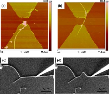
In an alternative approach to circumventing the unreliable manipulation of objects with the AFM, Li et al. have developed a system that generates real-time force feedback to the operator through a haptic joystick, Reference Li, Xi, Yu and Fung127 that is also used to update AFM scans of the surface. Reference Li, Xi, Chen, Pomeroy and Prokos128 The development of this technology Reference Xi and Li129 has culminated in a corrective fabrication technique, wherein CNTs are assembled near electrodes by dielectrophoresis before being repositioned to bridge the electrode gap [see Figs. 13(a) and 13(b)]. Reference Zhang, Member, Xi and Chen130 Using this technique of nanorobotic manipulation, they were able to build and test single-walled, multi-walled, and bundles of CNTs onto electrodes to operate as functional infrared sensors.
(a, b) An AFM probe with a haptic force feedback is used to move a CNT on the surface between two electrodes to create an infrared sensor. Reproduced from Ref. Reference Zhang, Member, Xi and Chen130. AFM images (a) before and (b) after the nanomanipulation show the successful transfer. (c, d) SEM images of the bending of a carbon nanofiber with an STM probe in a 4-probe STM system. Reproduced from Ref. Reference Qin, Kim, Wang and Li119.

In many cases, visualization is realized by building the manipulators into an SEM setup to give operators real-time visualization of the objects they are controlling. This is a common combination for microgrippers, but has also been used using SPM probes. For example, in the work by Qin et al., carbon fibers are pushed, bent, burnt, and broken under the real-time observations of the SEM [see Figs. 13(c) and 13(d)]. The combination of these machines could prove useful to researchers, who can take measurements and images of their devices during processes driven by the probe tips.
The need for active engagement of a human operator with these different mechanisms to ensure successful manipulation of nano-objects makes industrial adaptation impractical at present, with the best applications available in pure research. This problem may be solved if recognition and positioning of components can be automated by software. Additionally, mechanical manipulations are primarily limited to the 2D rearrangement of existing nano-objects, which limits the scope for 3D manufacturing.
C. Electrokinetic nanomanipulation
A force can be exerted on charged objects in solution when in a DC electric field, an effect known as electrophoresis, which allows for straightforward manipulation of particles toward charged surfaces. These charged surfaces are easily created by the application of a DC voltage between electrodes, Reference Xiong, Makaram, Busnaina, Bakhtari, Somu, McGruer and Park131 although alternative methods of charge patterning down to hundreds of nanometers can also be used to direct the 2D assembly of components. Reference Park, Lee, Unarunotai, Sun, Dunham, Song, Ferreira, Alleyene, Paik and Rogers132–Reference Zhou, Liu, Zhu, Lin, Pan, Jing and Wang134 Electrophoresis has been criticized for being limited to the manipulation of charged objects. However, the ability to functionalize nanoparticles with surface monolayers Reference Mark, Gibbs, Lee and Fischer15 enables a wide variety of nanoparticles to be manipulated. It should be noted, though, that some researchers have encountered problems when attempting to assemble films with DC or AC fields alone. Reference Yilmaz, Kim, Somu and Busnaina135
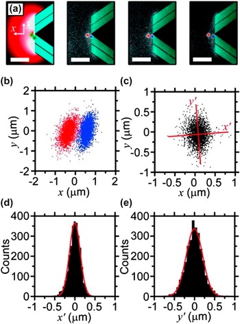
Analogously, dielectrophoresis refers to the force generated on a neutral particle when it is in an AC electric field: the electric field polarizes the particle, which in the nonuniform field results in a nonzero Coulomb force acting on the particle. Although two electrodes are usually required for dielectrophoresis, Reference Wood, Wolsiefer, Cohn and Williams136 the use of a triaxial probe to generate a dielectrophoresis field that acts as a non-contact trap for dielectric nanoparticles has been recently demonstrated Reference Brown and Westervelt137,Reference Brown and Westervelt138 (see Fig. 14). This method is proposed to work for particles as small as 5 nm Reference Brown and Westervelt138 and has been verified for the isolation of 100 nm polystyrene beads. Reference Brown and Westervelt137 The non-contact manipulation of nanoparticles in 3D can thus be achieved, with the probe moving the particle through the solution and releasing it on command. However, the strength of the trap limits the positioning accuracy of the particles in the solution, with the polystyrene beads having standard deviations of 133 nm and 204 nm in the x and y axes from the intended location. The increasingly strong influence of Brownian forces will only exacerbate this problem as the manipulated particles become smaller. However, if the electric field confining the particle could be amplified, then its position might be more easily confined, and the accuracy improved. Despite the initial problems, this method represents one of the most impressive results within nanoparticle manipulation.
Non-contact capture of 200 nm polystyrene beads by a triaxial probe by dielectrophoresis. Reproduced from Ref. Reference Brown and Westervelt137. (a) Schematic and three representative fluorescence images of a 100 nm radius bead trapped in the negative-dielectrophoresis trap. (b) Scatter plots of the position of the bead in the trap (red dot) and the tip inferred from the position of an attached bead (blue dot). (c) Scatter plot of the separation between the trapped bead and the triaxial tip given by the separation of trapped bead/adhered bead pairs. The axes of tightest and loosest trapping are determined with principal component analysis and are shown on the plot as the x-axis and y-axis, respectively. (d) Histogram of the spread of the trapped bead about the x-axis. (e) Histogram of the spread of the trapped bead about the y-axis.

D. Optical nanomanipulation
The energy profile of a laser can be used as an optical trap for metallic and dielectric nanoparticles, capable of 3D manipulation. The forces exerted by these optical tweezers are only of the order of piconewtons, generally making it useful only for objects immersed in liquid media, which has seen it used primarily for manipulating biological entities. Reference Jonás and Zemánek139 Recent advances are now allowing the manipulation of nanoscale objects, Reference Tong, Miljković and Käll140–Reference Yan, Shah, Chado, Gray, Pelton and Scherer143 like gold nanoparticles Reference Guffey and Scherer141 and silver nanowires Reference Yan, Shah, Chado, Gray, Pelton and Scherer143 arbitrarily positioned onto surfaces. The error in the positioning of these particles, however, was untenably high for reliable fabrication practices e.g., 40 nm particles with deposition errors in the order of hundreds of nanometers. Reference Guffey and Scherer141 This limitation to the tweezers is unfortunate, given the flexibility of manipulation it offers such as using the polarization of the light to orient and align the objects. Reference Tong, Miljković and Käll140,Reference Yan, Sweet, Jureller, Guffey, Pelton and Scherer142
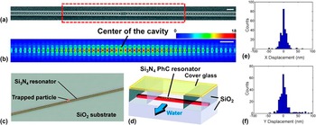
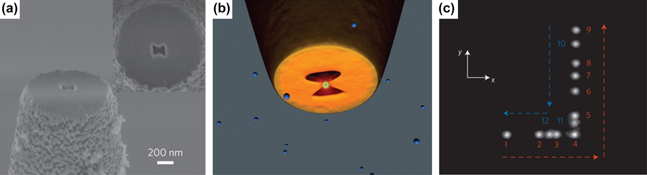
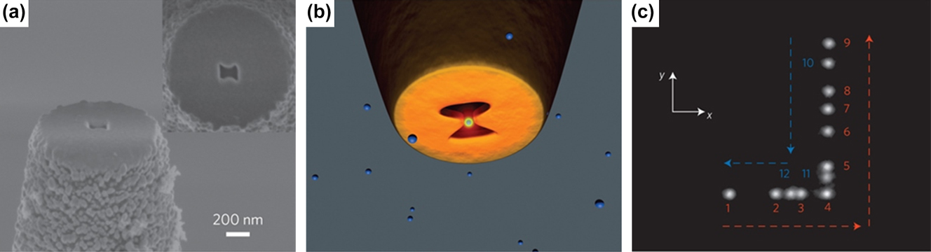
The precision of this placement can be improved though: for instance by coupling the laser with cavities in an optical resonator, it has been demonstrated that even 22 nm polymer particles can be immobilized in the cavities Reference Chen, Serey, Sarkar, Chen and Erickson144 (see Fig. 15). Because these cavities increase the electric field density within them when the laser is on, with positioning error typically within 25 nm achieved. This is comparable to the accuracy of the self-assembly approach to single-particle placement. Reference Huang, Bhadrachalam, Ray and Koh145 The use of these nanoapertures also benefits from a low increase in temperature of approximately 0.3 K, which helps limit the attraction of multiple particles to the aperture by thermophoresis and avoids damaging biological entities during manipulation. Following a similar design practice, 50 nm polystyrene beads have recently been trapped in a nanoaperture on an optical fiber and manipulated in suspension over several micrometers Reference Berthelot, Aćimović, Juan, Kreuzer, Renger and Quidant146 (see Fig. 16). This near-field optical nanotweezer is able to both manipulate and track the particle in 3D through the same fiber, allowing a facile means of manipulating dielectric nano-objects, even though the wave length of the laser used was more than 21 times the diameter of the bead. Additionally, the reflected signal collected by the fiber was able to make a distinction as to whether or not a particle was currently trapped at the tip. This represents an important leap forward into the nanoscale world for optical tweezers, almost certainly establishing the use of similar apertures for future mechanisms.
The capture of 22 nm polymer nanoparticles in a photonic crystal (PhC) resonator. Reproduced from Ref. Reference Chen, Serey, Sarkar, Chen and Erickson144. (a) SEM image of a silicon nitride PhC resonator. (b) FDTD simulation showing the electric field distribution near the resonator cavity (indicated by the red dashed lines in panel (a). The colors indicate the relative field intensity (arbitrary unit). Strong field enhancement can be seen within the small hole at the center of the cavity. Scale bars in (a) and (b), 1 μm. (c) Schematic showing trapping of a nanoparticle on a silicon nitride PhC resonator. (d) Schematic showing the relative locations of the resonator and the flow chamber. The resonator and the waveguides connected to the resonator are on the top of a silicon dioxide layer. The upper part of the resonator is exposed to the aqueous solution in the flow chamber, while the waveguides connected to the resonator are surrounded by silicon dioxide. (e, f) Histograms of the displacement of the trapped particle from the trap center in the X and Y direction.

The capture and manipulation of a 50 nm polystyrene bead with a near-field optical tweezer. Reproduced from Ref. Reference Berthelot, Aćimović, Juan, Kreuzer, Renger and Quidant146. (a) SEM image of an 85-nm-gap bowtie nanoaperture patterned at the extremity of a tapered optical fiber. (b) Schematic of experimental configuration. The 1,064 nm trapping laser is directly coupled into the fiber to excite the transverse mode of the bowtie nanoaperture. (c) Composite image reproducing the displacement of the trapped object. This displacement takes place over a 30 s time period with numbers 1–12 represent the successive steps of the tip and particle movement.
The plasmonic heating effect can nevertheless be put to good use: by exposing a gold nanoparticle embedded in a layer of PDMS to laser light, the localized heating cures the PDMS in proximity to the particle. Reference Fedoruk, Meixner, Carretero-Palacios, Lohmüller and Feldmann147 The laser also acted as an optical tweezer, which was able to move the particle around to draw 2D features into the PDMS, with no curing of the PDMS observed due to laser exposure alone, and producing PDMS nanowires of several micrometers in length and 120–130 nm in diameter. It remains to be seen if these features could then be used as a mask for further processing. There is also a difficulty that arises from continuously write with a nanoparticle without retracing previous paths used by the particle to prevent over-cured and thus over-sized features, to build full nanostructures. Any large scale patterning with multiple particles would also need to initially locate particles in the PDMS, and write structures whilst presumably not coming into proximity of other particles causing unintended curing. However, the potential to write 3D features in this manner is an exciting future area of research.
E. Self-assembly
By exploiting chemical processes through which materials bond to each other, it is possible to self-assemble features from the bottom-up with molecules and particles as the building block. The assembly of these components can be directed by a variety of interparticle forces, Reference Bishop, Wilmer, Soh and Grzybowski148 which are commonly used to create molecular monolayers on surfaces, which is extremely useful for thin film applications, Reference Sakakibara, Hill and Ariga149 and ordered arrays of nanoparticles. Reference Barrow, Funston, Wei and Mulvaney150 This has proven to be an extremely useful tool for nanofabrication, with an extensive body of research investigating the various methods and applications of self-assembly. Reference Barrow, Funston, Wei and Mulvaney150–Reference Bellido, Domingo, Ojea-Jimenez and Ruiz-Molina152
Combining multiple methods of self-assembly has even succeeded in the creation of an operational 3D motor from a single polymer crystal. Reference Dong, Zhou, Zhang and Li153 Successive self-assembly processes allowed a crystal of R-hydroxyl-ω-thiol-terminated polycaprolactone to be coated in three different types of nanoparticles: gold nanoparticles to facilitate optical visualization; platinum nanoparticles to drive the motor by catalyzing the decomposition of the surrounding hydrogen peroxide solution; and iron oxide nanoparticles to allow for remote magnetic guidance of the motor. The functioning motor is shown to perform all of these functions simultaneously, with attempts at moving around magnetic polystyrene microparticles proven partly successful. This type of study shows just how useful nanoparticles and self-assembly are to expand the functionality of complex devices.
However, the exact positions the molecules bond to in self-assembly requires careful engineering of the devices; lithography methods are vital to ensure that the assembly occurs in the right locations. Self-assembly is therefore not available as a standalone fabrication method that can build completely arbitrary assemblies, but it does allow for existing surfaces and objects to be functionalized to perform other useful tasks, Reference Sakakibara, Hill and Ariga149,Reference Galisteo-López, Ibisate, Sapienza, Froufe-Pérez, Blanco and López154–Reference Kraus, Malaquin, Schmid, Riess, Spencer and Wolf156 including large-scale growth of features like CNTs for circuits. Reference Park, Afzali, Han, Tulevski, Franklin, Tersoff, Hannon and Haensch157
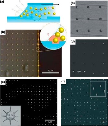
Patterning areas of a surface for self-assembly, although limited to the resolution of the preceding lithography steps, can even direct the very precise manipulation of nanoparticles individually. For instance, 60 nm gold nanoparticles were shown to be isolated onto a PDMS stamp by drawing a meniscus of gold colloid across the indented surface Reference Kraus, Malaquin, Schmid, Riess, Spencer and Wolf156 (see Fig. 17). As the nanoparticles that accumulated at the edge of the meniscus pass over the surface indents, individual nanoparticles are drawn into each dent by capillary forces while the Stokes drag of the meniscus pulls additional particles away. Transfer printing was then used to attach these gold particles to a separate PMMA coated substrate, transferring the majority of the pattern and allowing the PDMS stamp to be reused. Once hydrogen plasma cleaning has removed the PMMA film, the nanoparticles were shown to have retained their functionality for nanowire growth. Similar approaches to capillary driven assembly have also reported the capture of Au nanoparticles down to 2 nm in diameter. Reference Cui, Bjork, Liddle, Sonnichsen, Boussert and Alivisatos158 Since this technique can be extended to other types of nanoparticles, provided very good accuracy during transfer (reportedly within 100 nm of their captured locations) and a positioning error rate of less than 20 ppm, this approach to nanoparticle printing could be extremely useful in nanomanufacturing. It may also benefit from an update with some of the latest transfer printing techniques being developed. Reference Carlson, Bowen, Huang, Nuzzo and Rogers159
Single nanoparticle printing. Reproduced from Ref. Reference Kraus, Malaquin, Schmid, Riess, Spencer and Wolf156. (a) Schematic of the nanoparticle capture process: a colloid meniscus containing 60 nm Au nanoparticles is drawn across an indented PDMS surface. (b) A bright-field optical micrograph of the assembly in action; the bright line indicates the accumulation zone of nanoparticles in the colloid. (c, d) AFM topography scans of 60 nm Au nanoparticles (c) captured on the PDMS stamp and (d) printed onto a silicon substrate. (e) SEM image of detail (left eye) from a printed array of Au nanoparticles. (f) SEM image of silicon nanowires grown from a printed array of Au nanoparticles (inset is tilted).

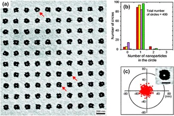
Unfortunately, capillary assembly makes it hard to control the exact location that nanoparticles will adhere to, which is very important to position particles in desired configurations. A more accurate method of isolating nanoparticles may instead be achieved by electrostatic interactions between a colloid and SAMs Reference Huang, Bhadrachalam, Ray and Koh145 (see Fig. 18). The proof-of-concept device worked by using patterned circular areas of a substrate with a SAM terminated by amino groups, and the surrounding area with a carboxyl terminated SAM: these two surfaces had a static surface charge in solution (relative to the pH level) as a result of protonation and deprotonation, respectively, such that the area inside the circle was positively charged and the area outside was negatively charged. Immersion of this gate in 20 nm colloidal gold nanoparticles capped with citrate ions that carry a negative surface charge in solution, resulted in the attraction of the gold toward the gates' positively charged area, with the surrounding negative charge funneling the gold nanoparticles to the center of the gates. Once one of these particles was bound to a gate, the negative surface charge of the gold nanoparticle opposed the approach of additional particles, which insured only single particle placement. This is an extremely impressive result considering that the diameter of the gate is almost 7 times larger than that of the particle it isolated and could have been even better if the lithographic definition of the gates was more accurate. It is entirely likely that a combination of the techniques of the gating mechanism Reference Huang, Bhadrachalam, Ray and Koh145 and transfer printing Reference Carlson, Bowen, Huang, Nuzzo and Rogers159,Reference Zheng, Lalander, Thai, Dhuey, Cabrini and Bach160 can be combined for electrically directed assembly Reference Porter, Abelmann and Bhaskaran161 ; incorporated into a probe configuration, this may be useful for the 3D printing of individual nanoparticles.
(a) Single nanoparticle capture in an array by self-assembly. SEM images of 20 nm Au particles self-assembled onto a surface patterned with gates. (b) Histogram of the number of nanoparticles captured on each of 400 tested gates. (c) Superimposed plot for the positions of single nanoparticles. Inset: SEM image of a gate containing one Au nanoparticle. Reproduced from Ref. Reference Huang, Bhadrachalam, Ray and Koh145.

In conclusion, single particle placement is able to build structures ranging from individual atoms up to hundreds of nanometers, but so far the throughput is very low and only useful for basic research and proof of concept designs. However, once commercially viable technologies have been discovered, increased automation will be able to increase the throughput. The possibility to combine self-assembly with one or more of the technologies described in this review is especially promising.
IV. DISCUSSION
It is clear that although ANM may not be suited to replace complementary metal–oxide–semiconductor (CMOS), it is likely that emerging processes can provide rapid prototyping capabilities as well as the ability to manufacture one-off parts and products. ANM has the potential to enable the manufacturing of specialized components at the nanoscale. This draws a close parallel with macroscale additive manufacturing that started off as an expensive tool, but is now being present in many school classrooms. Several ANM methods have been reviewed in this article, and we summarize the key capabilities of these in this section.
ANM covers a large spectrum of technologies each with their strengths and weaknesses. The criteria for successful ANM are design flexibility in the choice of materials and shape, resolution, writing speed/cost per unit, and initial investment cost. It is in the context of these criteria that future additive manufacturing techniques will be evaluated. As with all novel emerging technologies, it is worthwhile remembering that no one technology can provide the solution for all future manufacturing needs. However, in combination most of these needs can be met.
Single particle placement technologies such as STM, AFM manipulation, and optical tweezers are comparatively slow but they may be able to enable quantum computing Reference Fuechsle, Miwa, Mahapatra, Ryu, Lee, Warschkow, Hollenberg, Klimeck and Simmons118 or advance fundamental research through proof-of-principle device fabrication. Self-assembly is essentially how nature works and in the future it is likely that bio-inspired self-assembly in combination with ANM will create novel structures on a large scale. So far, self-assembly is in its infancy but as a tool to control wettability Reference Galliker, Schneider, Eghlidi, Kress, Sandoghdar and Poulikakos72 and adhesion Reference Park, Hardy, Kang, Barton, Adair, Mukhopadhyay, Lee, Strano, Alleyne, Georgiadis, Ferreira and Rogers16 or guide charged particles Reference Huang, Bhadrachalam, Ray and Koh145 SAMs have found extensive use. Reference Gooding and Ciampi162
DPN has been shown to offer an excellent selection of both organic and inorganic materials with sub-50 nm resolution. In the course of the development of this technology, the traditional cantilever structure has been replaced by cantilever-free systems and arrays of probes. So far, the resolution is limited by the size of both the tip and the meniscus forming between the tip and the substrate. For many biological applications, the current resolution is adequate; in fact, DPN is a powerful research tool for manipulating cells at subcellular resolution Reference Pulsipher and Yousaf163 and changing the growth conditions for these cells. This resolution is, however, not sufficient for the future of IC manufacturing, but closely related lithography methods such as local anodic oxidation reach sub-10 nm resolution Reference Martinez, Martinez and Garcia164 proving that better resolution is possible with DPN when combined with an electrically driven reaction. DPN has so far been a two-dimensional lithography technique but the technology is very flexible with an inbuilt imaging capability and extending it into the third dimension seems plausible in the near future.
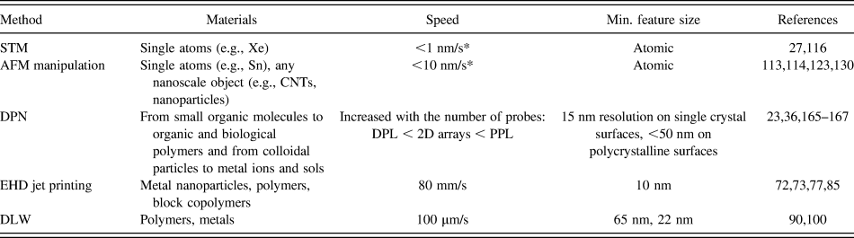
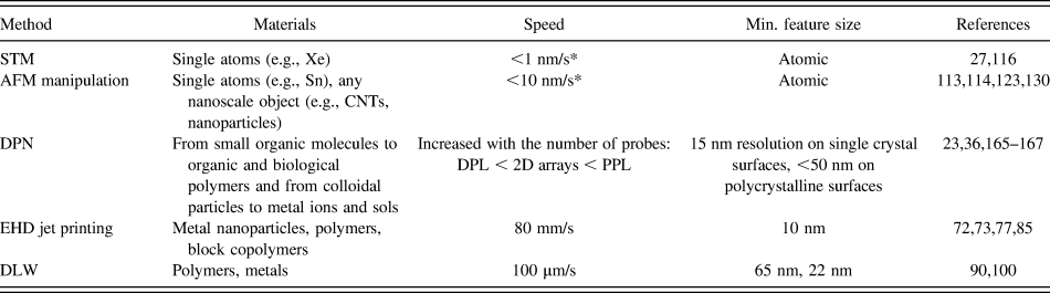
Electrohydrodynamic (EHD) jet printing has gone through a rapid development in the last couple of years with resolutions now reaching sub-50 nm Reference Galliker, Schneider, Eghlidi, Kress, Sandoghdar and Poulikakos72,Reference Bisht, Canton, Mirsepassi, Kuinsky, Oh, Dunn-Rankin and Madou77 or sub-10 nm when combined with block copolymer technologies. Reference Onses, Song, Williamson, Sutanto, Ferreira, Alleyne, Nealey, Ahn and Rogers73 The writing speed is unparalleled when compared to other additive manufacturing technologies presented here (see Table I) and is comparable to the writing speed of EBL. Additionally, EHD jet printing is capable of printing in three dimensions Reference Galliker, Schneider, Eghlidi, Kress, Sandoghdar and Poulikakos72 and because the material is deposited through a solvent, a wide range of materials can be available. The equipment requirements are basic, so equipment cost can be kept low. The main challenges are nozzle clogging and layer-to-layer alignment but these are not insurmountable problems making EHD jet printing a promising candidate for future ANM.
List of the materials, deposition speed, and minimum feature size reported for each ANM technology. * = Estimated.
DLW offers great flexibility and was one of the first technologies capable of 3D manufacturing at the nanoscale. It has proven invaluable for fabrication of 3D photonic structures and has already had commercial success. Despite this success, DLW has drawbacks particularly because material selection is still limited in spite of it being a relatively mature technology.
Direct write nanomanufacturing is still not able to produce the billions of structures needed for the IC industry, but neither is macroscale additive manufacturing able to compete with the cost per unit of injection molding and other mass-fabrication methods. Macroscale additive manufacturing first found a home in niche areas of dental and medical care, aerospace, automotive, and entertainment; nevertheless, macroscale additive manufacturing is on the rise and the market is predicted to double from 2011 to 2015. Reference Feenstra, Schaefer, Jay and Scudamore1 ANM will have to start out with markets smaller than IC manufacturing and the smaller investment needed for ANM equipment will help this development.
Currently an IC manufacturing plant costs around $9 billion; an ANM unit at <$500,000 would be transformational for small and medium size firms to own their manufacturing facilities. Additionally, the way designers think will change as 3D structures become readily available and the low material waste enables the use of expensive materials such as proteins in biosensors. There is also a potential environmental gain to using ANM over planar device fabrication as a traditionally built 2 g silicon chip requires 1.6 kg of fossil fuel, 73 g of chemicals, and 32 kg of water. Reference Williams, Ayres and Heller20,Reference Williams168 Research into additive nanomanufacture could focus on cutting this environmental impact, for example by eliminating waste by directly placing materials where needed. Additionally, ideas that previously had no future because the market did not require the millions of sold units needed to break-even may now become viable. The unit price of direct writing does not depend on the density of the printed structures, as is the case for planar device fabrication, but rather depends on the total printed area. For a chemical or biomarker sensor, the detector area might be much smaller than the minimum die size and planar manufacturing could become prohibitively expensive.
The aspect of resolution as compared to semiconductor manufacturing is also seeing progress; the resolution of some of these techniques has reached a level where it can compete with that of EUV-lithography. They are well suited to a range of materials, not just “CMOS-compatible” materials; Table I summarizes a subset of the available materials possible in each of these technologies.
The future of ANM relies on these technologies to either enable fabrication of structures that cannot otherwise be built or add functionality to existing technologies. One example where ANM can enable new structures is the assembly of nanoparticles into functional devices. It has been shown that a wire of gold nanoparticles can be used as single electron transistors Reference Kane, Inan and Saraf169 but it is currently almost impossible to mass-manufacture such structures. Probe-based pick-and-place ANM can accurately position nanoparticles in the desired configuration making such devices possible in the future (see Fig. 19). Phase change memory devices are another example where ANM might enable a new technology. The device is a 3D structure which is inherently difficult to fabricate using planar technologies and the ability to build these structures from individual nanocomponents using ANM is a real possibility. Promising biological applications of macroscale additive manufacturing are 3D scaffolds for bone and tissue growth, Reference Bonzani, George and Stevens170,Reference Pham, Sharma and Mikos171 direct printing of cells for organ growth as well as creating biocompatible films for drug delivery. Reference Wang, Wang, Yin and Yu172 At the nanoscale, ANM has the capability to fabricate structures from a subcellular level to sizes suitable for cellular scaffolds (cells are 1–100 µm in diameter). Biological applications of ANM include bioarrays for screening, micro- and nanoscale robotics, biosensing, and biocompatible environments for cell growth. In biology, multiplexing is of great importance due to the vast amount of proteins and small molecules found in living organisms. One of the challenges for bio-ANM will be to deposit single molecules; the ability to add parts of molecular functional elements, such as ion channels or molecular motors using ATP to harvest energy, will enable the study of individual cellular reactions or the creation of bionic micro-robots. Biocompatibility is an area of importance for bio-scaffolds and stem cells have especially proven difficult to grow in vitro. The growth is affected by cell adhesion to the substrate, chemical growth, small-molecule extracellular signaling and mechanical strain. Reference Brafman173 ANM technologies such as EHD jet printing have the ability to print protein fibers with subcellular resolution Reference Nuansing, Frauchiger, Huth, Rebollo, Hillenbrand and Bittner83 which could solve some of the biocompatibility problems and potentially accelerate growth in the field. The challenge will be to build biocompatible or living structures in three dimensions rapidly for medical applications. For electrochemical electrode array-based biosensing, smaller dimensions increase sensitivity via better signal-to-noise ratio, lower detection limits, and superior temporal resolution. Optimizing this electrode array design can improve diffusion of the reactive species to the electrode array or increase the surface area for increased sensitivity and it will be a challenge for ANM to show the flexibility to improve biosensing through design and material choice.
ANM in the coming decade is likely to fabricate single electron transistors, multiplexed bioarrays, and 3D phase change memory. Devices and sensors could be directly printed on existing technologies within aeronautical, automotive, medical, and optical industries.

Direct writing of graphene might also be possible in the future by allowing an AFM tip coated with graphite to slide over a surface, thereby leaving a nanoribbon/monolayer of exfoliated graphene. This would be an improvement of the results by Zhang et al. Reference Zhang, Small, Pontius and Kim174 who used a mounted graphite block on the cantilever as the tip of an AFM to transfer thin graphite samples onto a SiO2/Si substrate. “Writing” with the nanopencil yielded slices of graphite just a few tens of atomic layers thick, thereby almost succeeding in direct writing of graphene. This could enable device fabrication and repairing or modification of existing circuits to tailor functionality. Other areas in which ANM can solve fabrication challenges in the future are photonic crystals, metamaterials such as negative refractive index materials and invisibility cloaks, electrochemical reactors, and high-density electronics.
ANM can also be used to add functionality to existing structures in the future. For example, electronics could be printed directly at the end of an optical fiber thereby integrating optics and electronics in ways never seen before, and sensors can be printed directly onto engine parts or medical devices. ANM would also enable fully integrated devices including electronic, optical, and biochemical elements.
In conclusion, we have reviewed both single particle placement and direct writing technologies able to create sub-100 nm structures. We have especially focused on their ability to create heterogenous structures from multiple materials and the possibility to extend fabrication into the third dimension. We identified single particle placement technologies such as STM, AFM manipulation, and optical tweezers as enablers of technological advances but not as future manufacturing tools. Direct writing technologies, on the other hand, offer a much more promising future of design flexibility, high resolution, and high throughput. DLW offers high geometrical flexibility and medium throughput but currently suffers from a poor selection of materials. DPN is a reasonably mature technology with a wide material selection and promises of sub-10 nm resolution. The technology can be scaled up and currently the main challenges are to print in three dimensions and combine more functional materials. EHD jet printing is a simple and inexpensive technology that offers writing speeds comparable with e-beam lithography with high resolution (∼20 nm) and great material choice. Additionally, 3D structures of only 50 nm wide have been printed proving the possibility of true 3D ANM.
Within the next few years, we predict a rapid development of the ANM technologies presented here, especially toward 3D ANM. This new capability will inevitably lead to more innovation as new applications emerge. If ANM follows the development trajectory of the last decade, its rise as a nanoscale rapid prototyping tool will soon be imminent.
ACKNOWLEDGMENTS
This review was made possible by an EPSRC Manufacturing Fellowship “Additive nanomanufacturing via probe-based pick-and-place nanoparticle assembly,” Grant EP/J018694/1.