I. INTRODUCTION
Since the large scale production of integrated circuits in the 1960s, thin film materials for microelectronic devices have become a major topic in the modern materials science community. The ongoing performance increase with the number of transistors and switching frequency coupled with the miniaturization of semiconductor components require sophisticated deposition processes and excellent film material properties. Reference Moore1 In many silicon-based microelectronic devices, increasing power densities lead to significant temperature rises up to ∼400 °C within the microsecond regime during switching operations. Reference Nelhiebel, Illing, Schreiber, Wöhlert, Lanzerstorfer, Ladurner, Kadow, Decker, Dibra, Unterwalcher, Rogalli, Robl, Herzig, Poschgan, Inselsbacher, Glavanovics and Fraissé2 This results in large thermal stresses due to different coefficients of thermal expansion (CTE) of the materials, where plastic deformation can occur if the yield stress of the metallization is reached. Reference Flinn, Gardner and Nix3 Such a repetitive dynamic temperature rise leads to a thermo-mechanical damage of the metallization in the form of severe surface roughening and voiding. These features can result in local excess temperatures leading to a thermal runaway and local melting of silicon. Reference Nelhiebel, Illing, Schreiber, Wöhlert, Lanzerstorfer, Ladurner, Kadow, Decker, Dibra, Unterwalcher, Rogalli, Robl, Herzig, Poschgan, Inselsbacher, Glavanovics and Fraissé2
To overcome these problems, one key concept of metallization development is to increase the film thickness (h f), which leads to a greater specific heat capacity and longer operational lifetime. In a previous study, it has been shown that increasing the copper metallization thickness to 20 µm will result in the largest relative benefit gain such as the maximum peak temperature during a power pulse. Reference Nelhiebel, Illing, Detzel, Wöhlert, Auer, Lanzerstorfer, Rogalli, Robl, Decker, Fugger and Ladurner4 Copper, used in modern power semiconductor metallization schemes, Reference Robl, Melzl, Weidgans, Hofmann and Stecher5 exhibits very interesting structural properties. Besides its excellent electrical and thermal properties, copper has a very low stacking fault energy (SFE) resulting in a high number of twin boundaries, Reference Zhou and Wadley6 as well as a large elastic anisotropy factor. Reference Wikström and Nygårds7 These attributes result in a large variety of initial microstructural characteristics, such as grain size, d, and texture, because they are directly coupled to the corresponding film thickness. Reference Thompson and Carel8 In copper films, a pronounced texture transition from a dominating {111} texture at small thickness (<1 µm) to a high fraction of {100}-oriented grains at greater film thickness (5–10 µm) can be observed, as well as a different grain size distribution between the two texture components. Reference Sonnweber-Ribic, Gruber, Dehm and Arzt9 These initial microstructural differences in thicker Cu films lead to the presumption that regardless of the chosen fatigue experiment, the microstructural evolution and related fatigue damage in copper films will depend on the particular film thickness.
In the literature, numerous studies report on the (thermo)-mechanical fatigue of copper films in the range of h f = 0.1–5 µm on thick substrates. Reference Zhang, Volkert, Schwaiger, Wellner, Arzt and Kraft10–Reference Zhang, Volkert, Schwaiger, Arzt and Kraft19 Fatigue damage, which is often described by extrusions/intrusions and severe roughening on the film surface, is directly correlated to film thickness where the height and extrusion density decrease with decreasing thickness. Reference Zhang, Schwaiger, Volkert and Kraft16 Other studies attribute localized differences in the fatigue damage to the distinctly different behavior of {100} and {111} out-of-plane oriented grains. Reference Heinz, Robl and Dehm13,Reference Zhang, Schwaiger, Volkert and Kraft16,Reference Aicheler, Sgobba, Arnau-Izquierdo, Taborelli, Calatroni, Neupert and Wuensch20–Reference Baker, Kretschmann and Arzt22 Although mechanisms are not fully understood, authors emphasized that dislocation substructures (e.g., {100} walls) being more likely in {100}-oriented grains, Reference Zhang, Schwaiger, Volkert and Kraft16 and the large difference in grain resolved in-plane stress σ (σ111/σ100 ∼ 2.3) due to elastic anisotropy, Reference Baker, Kretschmann and Arzt22 are potential reasons why film microstructures with a different fraction of {100} and {111} grains behave differently with respect to fatigue testing.
The question arises as to which thermo-mechanical behavior can be observed when h f ≥ 5 µm, where the fraction of {100}-oriented grains is expected to significantly increase. Reference Sonnweber-Ribic, Gruber, Dehm and Arzt9 The current literature on Cu foils indicates a lower tensile strength for 20 µm foils due to the increase of the soft {100} texture component but does not provide results with respect to thermo-mechanical fatigue. Reference Akiniwa, Suzuki and Tanaka23 Presented here are experimental results of thick thermo-mechanically loaded copper films, ranging from 5 to 20 µm film thickness and with various initial film textures. The local microstructural evolution, which is based on a site-specific tracking method, Reference Bigl, Wurster, Cordill and Kiener24 in combination with wafer curvature measurements, local scanning electron microscopy (SEM) studies, and surface roughness measurements is used to evaluate the film thickness influence upon thermo-mechanical fatigue.
II. MATERIALS AND EXPERIMENTAL
A. Materials synthesis and preparation
All samples were prepared via sputter and electrochemical deposition. First, a tungsten-based (∼100 nm) adhesion layer was sputtered on 725 µm thick silicon wafers with a (100) orientation, followed by a 300 nm sputtered Cu seed layer. On the top of the seed layer, electrochemical deposition was used and the deposition time was adjusted so that the final copper film thicknesses of 2.5, 5, 10, and 20 µm were obtained. The electrolyte was designed to result in an almost impurity-free Cu film. Reference Wimmer, Smolka, Heinz, Detzel, Robl, Motz, Eyert, Wimmer, Jahnel and Treichler25,Reference Bigl, Schöberl, Wurster, Cordill and Kiener26 All samples were subjected to a 30 min heat treatment at 400 °C in a reducing atmosphere (forming gas) to establish a stable room temperature microstructure.
B. Experimental techniques
The basic thermo-mechanical characterization of the films was performed using a wafer curvature system for in situ film stress characterization up to 1000 °C. Reference Bigl, Heinz, Kahn, Schoenherr and Cordill27 With a multiple optical beam sensor, kSA multibeam optical sensor (MOS) (k-Space Associates, Inc., Dexter, Michigan), the film stress evolution was measured from room temperature to 400 °C using a heating and cooling rate of 10 °C/min.
To experimentally simulate rapid temperature rises comparable to thermo-mechanical loading of the copper metallizations by high power pulses in power electronics, samples with lateral dimensions of 7 × 7 mm were thermally cycled in a custom-built fast thermal laser cycling device in an reducing atmosphere (forming gas, chamber pressure ∼160 mbar). Reference Wurster, Bigl, Cordill and Kiener28 The samples were thermo-mechanically loaded between 170 and 400 °C, resulting in a total applied thermal strain of about 0.7% per cycle due to the CTE mismatch using the average CTE values for Cu and Si in the corresponding temperature range. Reference Hahn29,Reference Swenson30 One laser cycle corresponds to an average heating rate of 1050 °C/s and a cooling rate of 110 °C/s with a total cycle time of approximately 2 s. For details on the cycling process, see Refs. Reference Bigl, Wurster, Cordill and Kiener15 and Reference Wurster, Bigl, Cordill and Kiener28.
After marking the film surface with Vickers orientation indents, the surface and microstructural evolution within a representative surface area were studied using a Dimension 3100 (Bruker, Inc., Billerica) atomic force microscope (AFM) and a SEM LEO 1525 (Zeiss, Inc., Oberkochen, Germany) with electron backscatter diffraction (EBSD) analysis. For more information about the site-specific evaluation, see Ref. Reference Bigl, Wurster, Cordill and Kiener24. Between thermal cycling, samples were subjected to a selective etch to remove any copper oxide using a 100 vol% acetic acid solution at 35–40 °C for 2–4 min. Reference Chavez and Hess31 AFM images were made in the tapping mode and postimage analysis was performed using the Gwyddion 2.45 software. Reference Nečas and Klapetek32 For EBSD investigations, depending on the grain size, the scan size varied from 120 × 120 to 500 × 500 µm2 with a step size between 0.2 and 0.9 µm. For all scans, an acceleration voltage of 20 kV and a 120 µm aperture size were used and post-EBSD analysis was performed with the TSL Analysis v5 software. SEM micrographs were obtained using the secondary electron mode with a 20 µm aperture size and 6 kV acceleration voltage.
III. RESULTS AND DISCUSSION
A. Initial microstructural analysis
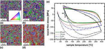
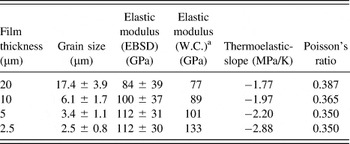
The specimens in the as-received state showed a clear film thickness dependence with respect to the initial grain size and texture for h f ≥ 5 µm (Fig. 1). A randomly oriented polycrystalline grain structure was obtained for h f = 2.5 and 5 µm [Figs. 1(a) and 1(b)]. With increasing film thickness, a predominant {100}-texture was observed for h f = 10 µm [Fig. 1(c)] and for h f = 20 µm [Fig. 1(d)]. The stereographic colored triangle in Fig. 1(a) was used for every grain orientation map (EBSD image) in this study. The grain size is a function of film thickness (see Table I). An average grain size of 2.5 ± 0.8 µm (including primary twin boundaries) was observed for the thinnest Cu film (h f = 2.5 µm) and d increased to 17.4 ± 3.9 µm for h f = 20 µm. The initial {100} out-of-plane orientation fraction scales linearly with h f and a significant increase of the grain size (including primary twins) was observed. This is in good agreement with the literature, Reference Thompson and Carel8,Reference Sonnweber-Ribic, Gruber, Dehm, Strunk and Arzt33 where driving forces such as the minimization of interfacial energy Δγi and strain energy ΔW ε explain the increase of the grain size and preferable {100} out-of-plane direction, respectively. Observations of the present films indicate that the texture transition does occur at thicknesses greater than 5 µm since the texture appearance [Figs. 1(a) and 1(b)] of the h f = 2.5 µm Cu film is almost identical to h f = 5 µm, which deviates from other studies where the transition thickness was found to lie between 3 and 5 µm and the absolute {100} texture strength was different with respect to h f. Reference Sonnweber-Ribic, Gruber, Dehm and Arzt9 The 2.5 µm thick film is used here only to illustrate the differences between thin films (≤5 µm) and thick films (≥5 µm), which is the focus of this paper.
(a–d) Initial film microstructures of the 2.5, 5, 10, and 20 µm copper films presented by grain orientation maps with IQ analysis. (e) The initial thermo-mechanical behavior changes as a function of film thickness. Standard IPF triangle is valid for all EBSD images.

Initial film properties of the four Cu film thicknesses.

a W.C. stands for wafer curvature measurements.
To study the change in texture in a quantitative manner, columnar grains are assumed and the mean elastic modulus is calculated. By taking the elastic constants of the stiffness tensor for copper (c 11: 168.4 GPa, c 12: 121.4 GPa, c 44: 75.4 GPa), Reference Ledbetter and Naimon34 the mean elastic modulus as a function of the initial microstructures was calculated using the EBSD information (for detailed information see Ref. Reference Bigl, Wurster, Cordill and Kiener15). As shown in Table I, for h f = 2.5 and 5 µm thick films, the calculated mean elastic modulus is 112 GPa. These two films have an almost randomly oriented microstructure, where an elastic modulus of 109 GPa Reference Bigl, Wurster, Cordill and Kiener15 was determined. With film thicknesses greater than 5 µm, the average elastic modulus decreases due to the increase of the soft {100} out-of-plane texture component.
The basic thermo-mechanical behavior using the stress-temperature evolution [Fig. 1(e)] also varies as a function of film thickness. The biaxial film stress is shown between room temperature and 400 °C of the first cycle and between 80 and 400 °C of the second cycle. Starting with similar tensile film stresses, a maximum compressive stress of −190 MPa was observed for h f = 2.5 µm, which decreases to approximately 120, 80, and 60 MPa for h f = 5, 10, and 20 µm, respectively. In terms of the shape of the film stress hysteresis, an influence of the changing initial film texture was observed. The two random textured microstructures (h f = 2.5 and 5 µm) exhibit a very similar thermo-mechanical behavior and a gradual change from elastic to plastic film stress evolution is observed.
For film thicknesses ≥5 µm, the stress hysteresis changes to a very sharp elastic to plastic film stress behavior, most notably for h f = 20 µm. It can be seen that two pronounced elastic regions are present for the heating and cooling segments and are followed by plastic flow at an almost constant stress. The transition of the stress-temperature behavior can also be observed in the decrease of the thermoelastic slopes with increasing film thicknesses (Table I). To quantify the correlation of the observed thermo-mechanical behavior with respect to film thickness, the elastic film modulus E f was determined in the temperature range of 90–110 °C (second cycle) using
 $${{{\rm{d}}{\sigma _{\rm{f}}}} \over {{\rm{d}}T}} \sim {{\Delta {\sigma _{\rm{f}}}} \over {\Delta T}} = \left[ {{{{E_{\rm{f}}}} \over {\left( {1 - {\nu _{\rm{f}}}} \right)}}} \right] \times \left( {{\alpha _{\rm{s}}} - {\alpha _{\rm{f}}}} \right)\quad ,$$
where the differential change of film stress as a function of sample temperature can be seen as the thermoelastic slope Δσf/ΔT. The corresponding stress slopes are the product of the biaxial modulus of the film, where νf denotes Poisson’s ratio of the film, and the thermal expansion mismatch between the substrate, αs, and the film, αf, in the given temperature range. As shown in Table I, the thermoelastic slopes decreased with increasing h f. The initial Poisson’s ratios of the films have been calculated (Table I) by calculating Poisson’s ratio for the three main orientations (〈111〉, 〈110〉, and 〈100〉) according to Refs. Reference Rösler, Harders and Baeker35 and Reference Zielinski, Vinci and Bravman36 (via calculating M [hkl] and E [hkl]). Corresponding Poisson’s ratios (ν〈100〉: 0.42, ν〈110〉: 0.44, ν〈111〉: 0.27) were then weighted using the fractional grain areas of the crystal orientations (〈111〉, 〈110〉, and 〈100〉) determined using the EBSD images (a maximum orientation tolerance of 8° was used). The remaining texture components were assigned to ν = 0.35 which can be attributed to a texture-free copper film. Reference Ledbetter and Naimon34 As shown in Table I, νf increases from νf = 0.35 in the two texture-free films (h f = 2.5 and 5 µm) to νf = 0.386 for the thickest copper film. The trend of Poisson’s ratio with respect to film thickness is quantitatively confirmed by the calculated elastic moduli in the range of 90–110 °C (using a Δα of 14.1 ppm/K Reference Bigl, Wurster, Cordill and Kiener15 ), where the decrease of E f correlates to the E determined from the EBSD measurements. The overall elastic film behavior relates to an increase of the softer {100} texture component for thicknesses between 5 and 20 µm.
In terms of the elastic properties, a good correlation between the wafer curvature and EBSD data was found for films thicker than 5 µm, considering that Cu has a temperature coefficient of elastic modulus of about −245 ppm/°C. Reference Ledbetter and Naimon34 However, for the 2.5 µm Cu film, a rather large discrepancy of the elastic modulus values (Table I) was found indicating that in thinner films (≤5 µm) other mechanisms overlap with the elastic response. It appears that the thermoelastic response for thin Cu films is inversely proportional to the film thickness and does not directly correlate to the initial elastic properties based on the microstructure and texture. The same behavior as the 2.5 µm film was also reported in another study where the thermo-elastic slope for 1 µm thin Cu films was found to be 3.6 MPa/K (in comparison, 2.88 MPa/K for 2.5 µm). Reference Flinn37
It was also observed that the stress relaxation behavior changed with increasing h f. While the two thinner Cu films (2.5 and 5 µm) showed distinct stress relaxation after reaching the maximum compressive film stress, the 20 µm thick Cu film illustrated plastic flow at an almost constant stress level of around −60 MPa/+35 MPa. Such a thermo-mechanical behavior is often referred as Al-type (e.g., passivated films), Reference Weiss38 where a thermally activated (stress driven) dislocation glide was proposed as the dominant deformation mechanism. Reference Flinn, Gardner and Nix3 Cu-type curves, for example, the stress-temperature behavior of the h f = 2.5 µm, use creep mechanisms such as power law breakdown or diffusional creep, which involve atomic diffusion. Reference Cocks and Ashby39 Considering that diffusion paths such as grain boundaries and twins were found to scale inversely proportional with h f, the obtained results by wafer curvature would indicate a gradual change from a Cu-type to an Al-type with increasing h f.
B. Global microstructure evolution
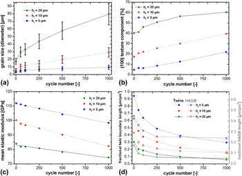
Since a large increase of the {100} out-of-plane texture component as well as different thermo-mechanical behavior can be observed with Cu film thicknesses ≥5 µm, samples with h f = 5, 10, and 20 µm were thermo-mechanically cycled up to 1000 cycles with the fast thermal laser cycling device. In Fig. 2, the global microstructural parameters of the three samples are shown as a function of cycle number. Figure 2(a) indicates that a significant grain growth occurs during thermal cycling in the three Cu films. In all three samples, the increase of the grain size (including twins) was the largest during the first 50 cycles followed by a constant increase up to 1000 thermal cycles. The grain size increased from 3.4 ± 1.1 µm up to 9.5 ± 2.8 µm (h f = 5 µm), from 6.1 ± 1.7 µm up to 29.1 ± 6.1 µm (h f = 10 µm), and from 17.3 ± 3.9 µm up to 79.5 ± 14.1 µm (h f = 20 µm).
(a) Grain size evolution of the 5, 10, and 20 µm thick Cu films as a function of cycle number and (b) the corresponding fractional area evolution of the {100} texture component. (c) Evolution of the mean elastic modulus determined from EBSD images. (d) Fractional twin/HAGB evolution with respect to the cycling state.

Figure 2(b) presents the fractional area of the {100} texture evolution as a function of thermal cycles. A similar steady (linear) texture increase for all three film thicknesses is seen, where the area fraction for h f = 5 µm increased from 5 up to 22%, for h f = 10 µm from around 17 up to 39%, and for h f = 20 µm the values increased from 40 up to 60%. As a result of the prominent {100} texture development, the average elastic moduli [Fig. 2(c), including linear fit lines] of all specimens decrease during thermo-mechanical cycling. The thinnest Cu film with h f = 5 µm shows a decrease of the mean elastic modulus from 112 GPa to 98 GPa, while the thicker films h f = 10 and 20 µm exhibit a decrease from 100 GPa to 82 GPa and from 84 GPa to 74 GPa, respectively.
To again quantitatively compare the three film thicknesses from an energetic point of view, a columnar grain structure is assumed. The biaxial strain, M, generated during cycling leads to different elastic strain energy densities, W, in the Cu films because the strain energy is orientation dependent in the elastic regime and described by Reference Thompson and Carel40
 $$W = {M_{hkl}}{\varepsilon ^2}\quad .$$
Using the elastic moduli from Fig. 2(c), the calculated initial biaxial moduli of M 5 µm, M 10 µm, and M 20 µm are 172 GPa, 157 GPa, and 137 GPa, respectively, can be determined. After 1000 thermal cycles, the respective biaxial moduli were lowered to 154 GPa, 131 GPa, and 122 GPa, for 5, 10, and 20 µm film thickness, respectively. The as-received data from the 2.5 µm thick film are used as a reference because it exhibits an almost random texture. The minimization of elastic strain energy can be calculated by Reference Thompson and Carel40
 $$\Delta W = \left( {{M_{2.5\,{\rm{\mu m}}}} - {M_{{h_{\rm{f}}}}}} \right){\varepsilon ^2}\quad .$$
Applying Eq. (3) leads to a reduction of the elastic strain energy after 1000 cycles of about 18 × ε2, 41 × ε2, and 50 × ε2 GJ/m3, compared to a randomly oriented polycrystalline film, for h f = 5, 10, and 20 µm, respectively. The reduction of the elastic strain energy emphasizes the dominant effect of the {100} out-of-plane grain growth. Considering that the 〈100〉 orientation has a M 100 = 115 GPa, Reference Sonnweber-Ribic, Gruber, Dehm and Arzt9 biaxial moduli calculated from the obtained EBSD analysis [Fig. 2(c)] reveal a transition from an elastically anisotropic microstructure to an isotropic structure with increasing film thickness and cycling stage.
The evolution of the fractional (primary) twin boundary and high angle grain boundary (HAGB) lengths are both presented in Fig. 2(d), where the total measured boundary length is divided by the total scan area. This results in a quantitative parameter with respect to twin migration as a dominant plastic deformation mechanism, Reference Field, True, Lillo and Flinn41 as well as indicating energy minimizing processes related to grain boundary energy. The fractional twin boundary length for h f = 5 µm decreases from 0.94 to 0.30 µm−1, for h f = 10 µm from 0.63 to 0.16 µm−1, and for h f = 20 µm from 0.30 to 0.06 µm−1. With respect to the fractional HAGB length evolution, a reduction from 0.45 to 0.24 µm−1, from 0.29 to 0.10 µm−1, and from 0.17 to 0.05 µm−1 for h f = 5, 10, and 20 µm was obtained, respectively.
The presented results in Fig. 2(d) indicate a faster rate of interface energy minimization with increasing h f. For h f = 5 µm the grain boundary length per unit area decreased to less than half of its initial value, while for h f = 20 µm the HAGB was reduced by more than a factor of three. This leads to the conclusion that the minimization of γi is proportional to h f.
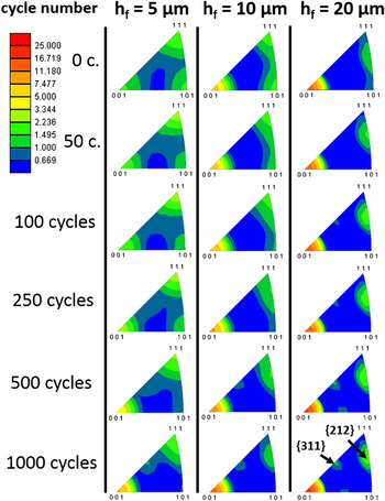
The texture evolution of the three films is presented in Fig. 3 with inverse pole figures (IPFs). The color code indicates the likelihood of the appearance of certain crystal orientations compared to a random orientation (blue/dark blue color). From the initial texture, it can be observed that with increasing film thickness the texture exhibits a gradual transition from a randomly oriented texture to a {100} dominated texture. During the cycling a texture increase of the {100} out-of-plane orientation, along with a slight increase of its {212} twin configuration, in all three film thicknesses occurs. The {110} plane orientation vanishes for all three thicknesses. After 1000 thermal cycles, only the {100} orientation with its corresponding {212}-oriented twin, a texture component close to the {311} orientation and the {111} out-of-plane orientation, is present where the fraction is significantly reduced with increasing film thickness. From Fig. 3 it appears that the {311} orientation develops due to a constant grain rotation and will be discussed in Sec. IV.
Inverse pole figures represent the texture evolution of the three different initial microstructures of the 5, 10, and 20 µm thick Cu films.

C. Local microstructure evolution
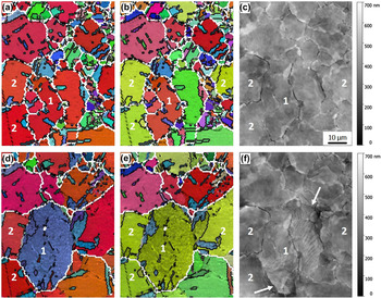
Many studies have already presented detailed work on the thermo-mechanical behavior of thinner films (≤5 µm). Reference Kraft, Wellner, Hommel, Schwaiger and Arzt11,Reference Heinz, Robl and Dehm13,Reference Schwaiger, Dehm and Kraft17,Reference Wurster, Bigl, Cordill and Kiener28 Here, microstructural observations are presented for the 20 µm thick film to emphasize the effect of film thickness, grain size, and texture on the thermo-mechanical behavior. In Fig. 4 the microstructural changes of the first 50 thermal cycles are presented for the same area using EBSD and AFM. The initial microstructure of the 20 µm film [Figs. 4(a)–4(c)] consists of many twinned grains (white lines indicate the HAGB and black lines indicate primary twins), where a significant portion has a {100} orientation in the normal direction (ND) to the film plane [Fig. 4(a)], but different in-plane orientations, as shown by the EBSD image showing the transversal direction [Fig. 4(b)]. Most of the grains exhibit pronounced grain boundaries, which can be seen in the AFM image [Fig. 4(c)]. After 50 cycles, significant changes in the microstructure can be seen by comparing the initial [Figs. 4(a) and 4(b)] to the after cycling grain orientation maps [Figs. 4(d) and 4(e)]. A group of grains with different out-of-plane and in-plane orientations collectively deform by shear, resulting in a crystallographic segment with an approximate {321} out-of-plane orientation, indicated by Feature 1. The {321} oriented segment is in a primary twin boundary relation with other growing grains (Feature 2). After 50 cycles, the newly formed twin segment [Figs. 4(e) and 4(f), Feature 1] and the surrounding grains have the same in-plane orientation [Fig. 4(e)]. From Fig. 4(f) it can be observed that the initial grain boundaries are still present and severe shear of the grains occurred on different glide planes. Furthermore, new HAGB interfaces are observed [Fig. 4(f), white arrows]. These findings suggest that grains in thicker films first reorient to compensate for the in-plane misorientation when a biaxial strain is applied and a collective reorientation of the former small grains occurs.
Local microstructural changes for h f = 20 µm, where the same area before (a–c) and after 50 thermal cycles (d–f), are presented. The crystallographic information with respect to the out-of-plane (a, d) and in-plane (b, e) directions is combined with the topographical information (c, f). Scale bar is valid for all figure parts.

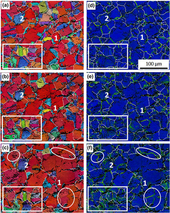
Figure 5 presents the microstructural changes for h f = 20 µm after 250, 500, and 1000 cycles [Figs. 5(a)–5(c)]. The microstructure of the selected area after the first 250 thermal cycles [Figs. 5(a) and 5(d)] is composed of a majority of large {100} out-of-plane oriented grains with their corresponding {212} oriented primary twins and smaller twinned grains with different orientations (see the highlighted rectangular section). Continued thermal-mechanical cycling resulted in a pronounced growth of {100}-oriented grains, causing large areas with the same crystallographic orientation (see Feature 1). The formation of crystal segments with low angle grain boundaries (LAGB) in the large {100}-oriented grains can be observed during the cycling. Additionally, kernel average misorientation Reference Calcagnotto, Ponge, Demir and Raabe42,Reference Wright, Nowell and Field43 images are provided [Figs. 5(d)–5(f)]. A local misorientation value of the kernel is assigned (2nd neighbor) with respect to the center of the kernel to indicate subgrain structures, such as LAGB, θ ≤ 15°, and plastic strain accumulation. The substructures, indicated by sharp green lines in the kernel average misorientation plots [Figs. 5(d)–5(f)], exhibit local misorientation angles of about six to twelve degrees. The circular features [Figs. 5(c) and 5(f)] highlight the geometric substructures with approximate angles of about 90, 135, and 150° between the straight LAGB domains. As seen from the grain orientation maps and kernel average misorientation plots, Feature 2 does not change the size despite the plastic strain accumulation during cycling. Grains and twins with an orientation other than {100} either significantly shrink or accumulate plastic strain during the thermal cycling. Such a behavior can be seen in the highlighted rectangular section where grains do not greatly change in the size but accumulate plastic strain during cycling. This is qualitatively indicated by the color changes [Fig. 5(c)] and the formation of a dense network of local misorientations [Figs. 5(d)–5(f)] in this area.
Microstructural evolution of h f = 20 µm illustrated by site-specific grain orientation maps with IQ analysis between 250, 500, and 1000 cycles (a–c). The corresponding kernel average misorientation plots are presented (d–f). Scale bar is valid for all micrographs.

The experimental results indicate that the mechanisms behind the grain growth during thermo-mechanical cycling are strongly influenced by h f and texture. The pronounced grain growth in the early stage (Fig. 4) was accomplished by collective shearing across the initial grains where it appears that the in-plane crystal orientation plays an important role. Experimental evidence is found in Fig. 5, where the same twin (marked as Feature 2) is preserved throughout the cycling experiment. The grain growth of the {100} texture component in the 20 µm thick film follows the development of defined grain substructures (circular features), while grains with other orientations have severe plastic strain accumulation. In a recent work, the authors found a similar behavior for a 5 µm thick Cu film cycled in an infrared furnace where such geometric substructures formed gradually from an initial misorientation gradient in an approximately{100}-oriented grain. Reference Bigl, Wurster, Cordill and Kiener15 The {100}-specific subgrain structures were also previously observed by others in thermally cycled submicron thick copper lines, where angles of 5–10° misorientation developed. Reference Mönig21 Transmission electron microscope (TEM) studies of mechanically fatigued copper films revealed that a grain size/film thickness dependent dislocation structure develops in {100} out-of-plane oriented grains. Reference Zhang, Volkert, Schwaiger, Wellner, Arzt and Kraft10,Reference Zhang, Schwaiger, Volkert and Kraft16 Geometric arrays of {100}-aligned dislocation walls form in larger grains due to the promotion of dislocation activity in larger crystals. Studies on the characterization of dipolar dislocation walls could be used to explain the geometry of the incurred LAGB substructures in the abnormally large 〈100〉 oriented grain. The authors Reference Charsley and Kuhlmann-Wilsdorf44,Reference Saxlová and Kratochvíl45 conclude that fatigue experiments in face centered cubic (fcc) metals, especially in crystals with a 〈100〉 crystal orientation suitable for multiple slip, would result in {100} and {110} walls. The model of combined (double) slip on the primary {111}/〈110〉 glide systems, where Burgers vectors of the slip systems add to a Burgers vector parallel or perpendicular to the dislocation walls, was used to explain the resulting arrays of edge dislocations. Reference Charsley and Kuhlmann-Wilsdorf44
D. Microstructural damage analysis
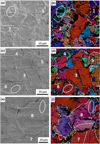
To qualitatively assess the thermo-mechanical fatigue damage, Fig. 6 presents representative areas after 1000 cycles of h f = 5–20 µm using SEM and EBSD micrographs. For the 5 µm thick Cu film [Figs. 6(a) and 6(b)], surface damage is present over the entire area. For example, pronounced glide bands formed within grains at twin boundary interfaces (Feature 1) and severe roughening can be observed at the HAGB (white lines) where hillock-like formations (Feature 2) at the grain boundaries are observed. The area in the circular marking is an example of extrusions/intrusions within individual grains.
Qualitative film surface damage analysis of h f = 5 µm (a, b), h f = 10 µm (c, d), and h f = 20 µm (e, f) using site-specific SEM and grain orientation maps with IQ analysis after 1000 thermal cycles.

With increasing film thickness, the surface damage changes. In the presented area for h f = 10 µm [Figs. 6(c) and 6(d)], large {100}-oriented grains exhibit pronounced shearing (slip) at their twin boundary interfaces after 1000 thermal cycles (Feature 3). Damage evolution differs depending on the grain orientation. For example, at Feature 4, the approximately {212}-oriented twin segment has severe surface roughening along preferred slip planes [Fig. 6(c)], while in the {100}-oriented twin counterparts the same fatigue features are not seen. Grains with an orientation other than {100} exhibited severe shearing at their twin planes and have a rougher appearing surface (Feature 5). Plasticity in the soft oriented {100} grains appears to accumulate differently than in other oriented crystal segments. The color gradients in Feature 6 [Fig. 6(d)] indicate a gradual change of orientation. The observation is that a gradual change in orientation across {100}-grains (constant tilt with respect to ND) occurs as a result of stress field minimizing LAGB. Reference Read and Shockley46 This suggests that dislocation reactions are involved in the crystal rotation which are energetically preferred compared to those that would result in glide steps at the film surface. In contrast to grains with orientations other than {100}, there was no dominant slip system activated that would lead to the formation of one specific slip pattern at the film surface.
For the Cu film thickness h f = 20 µm, it can be seen that thermo-mechanical fatigue damage strongly depends on the out-of-plane orientation. Feature 7 [Figs. 6(e) and 6(f)] shows that no significant surface damage is present in the {100}-oriented grains. Grains with crystal orientations other than {100} show severe surface roughening in the form of slip traces (Feature 8). The approximate {311} oriented grain and its twin show pronounced slip steps at the film surface, demonstrated by the circular marking at a twin boundary, and indicated by the mirror-like arrangement of the slip traces between the two crystallographic orientations. As already seen in Fig. 3, the ∼{311} out-of-plane orientation appears to develop due to a constant grain rotation, which is experimentally observed by Feature 8 in Fig. 6 where misorientation gradients are present across the twinned grain. This reorientation seems to also be strain energy driven as well, as reported by Zhang et al. on annealed Cu films on Si substrates. Reference Zhang, Xu and Ji47
Another study dealing with orientation specific damage analysis attributed the higher damage resistance of the {100} oriented grains to the lower biaxial stresses (σ111/σ100 = 2.26) as well as to the lower fraction of applied shear stress, τ, on a particular slip plane (eight equally active glide systems in 〈100〉 compared to six in 〈111〉). Reference Aicheler, Sgobba, Arnau-Izquierdo, Taborelli, Calatroni, Neupert and Wuensch20 Considering that after 1000 cycles d ≫ h f for thicker Cu films (h f = 10, 20 µm), grain to grain stress interactions are negligible and a single crystal approximation can be used (Schmid’s law). Reference Baker, Kretschmann and Arzt22 For such a condition, Mönig et al. computed the corresponding resolved shear stresses for each orientation, Reference Mönig21 where τ212/τ100 = 1.84. The {212} twin segment has two glide systems with the highest resolved shear stress compared to eight for the {100} parent grain which is in agreement with observed roughening in those twin sections [Figs. 6(c) and 6(d), Feature 4]. The experimental stress-temperature response [Fig. 1(e)] of the 20 µm thick film gives further proof to the assumption that the corresponding shear stresses on the eight equally active glide systems are very low. By approximating that the measured film stress σfilm corresponds to σ100, this would lead to a τ = S 100 × σ100 of about −24 MPa and 14 MPa in the heating and cooling stages, respectively.
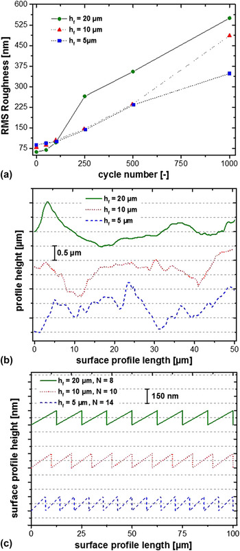
The site-specific damage investigation presented in Fig. 6 emphasizes that surface damage decreases with increasing film thickness. This can be directly correlated to the large fraction of {100} oriented grains which appear to have a higher damage tolerance with respect to thermo-mechanical fatigue. In Fig. 7(a) the root mean squared (RMS) roughness evolution is presented for the three thermally cycled Cu film thicknesses. The initially similar film roughness (88, 79, and 62 nm with increasing h f) evolves differently, where the RMS roughness was ranked with respect to the film thickness after 1000 cycles. This result may seem to contradict previous observations illustrated in Fig. 6, where the surface roughness appeared to be inversely proportional on h f. In Fig. 7(b) this contradictive observation regarding the surface roughness can be explained the following way. The representative surface profiles for h f = 5, 10, and 20 µm reveal that all film surfaces after 1000 cycles have a similar maximum vertical height amplitudes (Δy ∼ 1.5 µm), but the frequency of lateral surface roughness (which can be equated to surface damage) appears to increase with decreasing film thickness. This is due to the fact that R RMS is considered as an amplitude parameter and is only affected by vertical height variations of the film surface. Furthermore, the quadratic dependency of data points accentuates greater height variations providing greater R RMS values. Reference Gadelmawla, Koura, Maksoud, Elewa and Soliman48 To show the influence of the increasing fraction of more damage tolerant {100} grains with respect to increasing film thickness, 15 AFM profiles were taken after 1000 thermal cycles from each film thickness. The surface profile lengths, extracted by the AFM processing software, were numerically processed by creating a polygonal path using the Pythagorean theorem between each pair of data points. Reference Ahlberg, Nilson and Walsh49 The resulting mean surface lengths were normalized with respect to a profile length of 100 µm. This results in a mean surface length of 102.26 ± 0.65 µm, 101.53 ± 0.56 µm, and 101.22 ± 0.52 µm for h f = 5, 10, and 20 µm, respectively. To visualize these seemingly similar lateral roughness parameters, a reference roughness function was defined and used in Fig. 7(c), where the obtained surface length L (f) is defined as
 $${L_{{\rm{(f)}}}} = \left[ {d + \sqrt {{{\left( {{{100} \over N}} \right)}^2} + d} } \,\right]N$$
with d as the chosen roughness height and N giving the number of roughness intervals. This enables the direct comparison of accumulated surface damage with respect to the film thickness. From the graph it becomes evident that the Cu film with h f = 5 µm has the highest accumulated roughness. For the same reference profile length of 100 µm with a chosen roughness height of d = 150 nm, 15 intervals are required to obtain the experimental mean surface length. In comparison, the thicker films h f = 10 and 20 µm result in N = 10 and 8, respectively, indicating significantly less surface damage with increasing film thickness. The approach of numerically integrating several representative profile lengths over different AFM scans led to a statistical parameter with a physical meaning. Using a chosen reference function and displaying the accumulated damage with similar maximum height differences [see Fig. 7(b)] allow a direct qualitative and quantitative comparison of the film surface roughening (damage) of the three thermo-mechanically cycled film thicknesses [Fig. 7(c)]. The experimental observations from Fig. 6 are confirmed, emphasizing that fatigue damage is inversely proportional to h f for thick Cu films (h f ≥ 5 µm).
(a) RMS roughness evolution of the three film thicknesses as a function of cycle number. (b) Representative AFM profile sections after 1000 thermal cycles. (c) Reference surface roughness profiles using the determined mean surface length after 1000 cycles.

IV. CONCLUSIONS AND SUMMARY
In this study, the thermo-mechanical behavior of thick Cu films with thicknesses between 5 and 20 µm was presented. Initial microstructural characteristics of texture and grain size changed as a function of film thickness during 1000 thermo-mechanical cycles. The microstructural evolution during cycling and the corresponding surface damage is significantly different from similar studies on thin Cu films (<5 µm). The following conclusions can be drawn:
-
(1) Initial microstructural properties indicate that in electrodeposited Cu films, texture transitions toward the{100} out-of-plane orientation at film thicknesses ≥ 5μm occurs.
-
(2) Pronounced growth of the {100} out-of-plane orientated grains during thermal cycling was observed. The grain growth of the {100} texture component in thicker films (10 and 20 µm) agrees with a gradual formation of dislocation substructures.
-
(3) The thermo-mechanical fatigue damage assessment after thermal cycling (Fig. 6) revealed a transition of orientation independent surface damage (5 µm) to an orientation dependent damage (roughening) for thicker films (10 and 20 µm). A higher damage tolerance was found for the {100} oriented grains because these grains have a lower surface roughness.
-
(4) The accumulated surface roughness, displayed by the reference function (Fig. 7), indicates that fatigue damage has ∼1/h f dependency for thicker films (≥5 µm) and is different compared to thin Cu film counterparts (≤5 µm).
ACKNOWLEDGMENT
The work was performed in the project EPPL, financially supported by grants from Austria, Germany, The Netherlands, France, Italy, Portugal, and the ENIAC Joint Undertaking (ENIAC JU Grant Agreement No. 325608). This project is co-funded within the program “Forschung, Innovation und Technologie für Informationstechnologie” by the Austrian Ministry for Transport, Innovation and Technology.