Introduction
Thin films of semiconducting metal oxides are frequently used to modify the interfaces of organic semiconductor devices due to the large variety of materials with well-characterized optical and electronic properties and good chemical and physical stability.[Reference Greiner and Lu1] Metal oxide films deposited from nanoparticle (NP) suspensions in theory combine the properties of metal oxides with large-area and low-temperature processing, which not only improves compatibility with organic devices but also create processing challenges. For example, organic photovoltaics (OPVs) represent a promising route toward low-cost, lightweight renewable energy generation.[Reference Li, Baran, Forberich, Machui, Ameri, Turbiez, Carrasco-Orozco, Drees, Facchetti, Krebs and Brabec2, Reference Søndergaard, Hösel and Krebs3] Contact layers between bulk heterojunction (BHJ) active layers and electrodes can significantly improve performance of OPVs.[Reference Steim, Kogler and Brabec4] To fully realize the potential benefits of vacuum-free processing for low-cost OPVs, solution-processed contact layers are intensively researched in recent years.[Reference Li, Baran, Forberich, Machui, Ameri, Turbiez, Carrasco-Orozco, Drees, Facchetti, Krebs and Brabec2, Reference Søndergaard, Hösel and Krebs3, Reference Yip and Jen5, Reference Zilberberg, Meyer and Riedl6] Various solution-processed metal oxide films with high work function Φ have been utilized as hole contact layers (HCLs) in OPVs, which exhibit higher open-circuit voltage V oc,[Reference Steirer, Ndione, Widjonarko, Lloyd, Meyer, Ratcliff, Kahn, Armstrong, Curtis, Ginley, Berry and Olson7] higher fill factor FF,[6–12] and improved device stability[Reference Chen, Chen and Chuang9, Reference Zilberberg, Gharbi, Behrendt, Trost and Riedl10] compared with the well-established conducting polymer poly(3,4-ethylenedioxythiophene):poly(styrene sulfonate) (PEDOT:PSS) HCL.
Despite the recent progress, the stringent processing requirements of organic semiconductor devices have prevented general adoption of solution-processed metal oxide films as interfacial layers. For example, published reports on solution-processed metal oxide NP films as HCLs in OPVs typically require harsh post-deposition treatments, including annealing at temperatures >100 °C,[7–11,13–17] annealing for hours to days,[Reference Zilberberg, Trost, Schmidt and Riedl12, Reference Zilberberg, Trost, Meyer, Kahn, Behrendt, Lützenkirchen-Hecht, Frahm and Riedl18] and O2 plasma treatment,[Reference Steirer, Ndione, Widjonarko, Lloyd, Meyer, Ratcliff, Kahn, Armstrong, Curtis, Ginley, Berry and Olson7, Reference Steirer, Chesin, Widjonarko, Berry, Miedaner, Ginley and Olson13, Reference Stubhan, Ameri, Salinas, Krantz, Machui, Halik and Brabec15, Reference Stubhan, Li, Luechinger, Halim, Matt and Brabec16] all of which decrease compatibility with organic devices. We previously reported in situ oxidation of MoOx NPs in n-butanol to MoO3 with H2O2, but Φ after oxidation was still 0.3 eV lower than evaporated MoO3 films.[Reference Lee, Yi, Gao, Koerner, Park, Wang, Luo, Vaia and Hsu19] Alternatively, NP suspensions have been formed by dispersing metal oxide NP powders in alcohols with ultrasonication,[Reference Huang, Huang, Wei, Ho and Chu20] but this approach is limited by the availability of the powders and by NP size, typically >10 nm. Also, with a few notable exceptions,[Reference Steirer, Ndione, Widjonarko, Lloyd, Meyer, Ratcliff, Kahn, Armstrong, Curtis, Ginley, Berry and Olson7, Reference Steirer, Chesin, Widjonarko, Berry, Miedaner, Ginley and Olson13] most publications on solution-processed metal oxide NP HCLs have focused on n-type NPs.[8–12,14–20] Here, we demonstrate a general method to synthesize suspensions of ultrasmall (1–2 nm) MoO3, WO3, NiOx, and CoOx NPs in n-butanol. Spin-coated metal oxide NP films with no post-deposition treatment exhibit high Φ and ionization energy IE comparable with vacuum-deposited films and consistent with the oxidation states of the metal cations. Finally, we examine the performance of these NP films as HCLs in conventional and inverted poly[N-9′-heptadecanyl-2,7-carbazole-alt-5,5-(4′,7′-di-2-thienyl-2′,1′,3′-benzothiadiazole)]:phenyl–C71–butyric acid methyl ester (PCDTBT:PC71BM) OPVs.
Results and discussion
NP and film properties
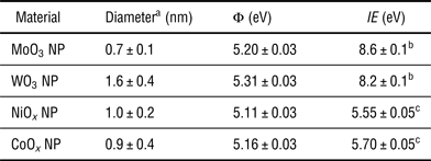
The metal oxide NP suspensions were synthesized by controlled oxidative dissolution of micron-sized metal powders in the presence of H2O2 and HCl, using a modification of published procedure.[Reference Redel, Huai, Dag, Petrov, O'Brien, Helander, Mlynarski and Ozin21] We found that by replacing the original solvent of water with n-butanol, and by reducing the metal concentration to 0.1 M, the diameter of the dispersed NPs measured using dynamic light scattering (DLS) was reduced from ~5 nm to 0.7 ± 0.1, 1.6 ± 0.4, 1.0 ± 0.2, and 0.9 ± 0.4 nm for MoO3, WO3, NiOx, and CoOx, respectively (Table I). The surfactant-free NP suspensions exhibit different colors arising from band gap and/or intraband d–d transitions of the metal oxides [Fig. 1(b) inset], and remain dispersed without change in DLS size for at least 2 weeks. Figure 1(a) depicts a typical transmission electron microscopy (TEM) image of NiOx NPs, showing spherical particles with diameter of 1.3 ± 0.7 nm, consistent with the DLS result. High magnification image of a single NiOx NP gives a characteristic spacing of 0.24 nm [Fig. 1(a), inset], which matches the spacing from (111) planes of NiO. Thus, oxidation of metal powder by H2O2 in n-butanol produces stable suspensions of ultrasmall metal oxide NPs.
(a) TEM images of NiOx NPs. Inset: high magnification image of single NP, showing lattice spacing of 0.24 nm. (b) Φ values for ITO and various films on ITO. The error bar for Φ measurement is 0.03 eV. Inset: photograph of metal oxide NP suspensions.

Properties of metal oxide NP suspensions and films.
aMeasured in suspension by DLS.
bMeasured by UPS.
cMeasured by PESA.
Metal oxide NP films spin coated on indium tin oxide (ITO) were characterized in air unless otherwise noted to examine their electronic properties. The Φ was measured using a scanning Kelvin probe, and was found to be 5.20 eV for MoO3, 5.31 eV for WO3, 5.11 eV for NiOx, and 5.16 eV for CoOx [Table I and Fig. 1(b)]. These values are significantly higher than the bare ITO (4.85 eV) and PEDOT:PSS (4.95 eV), and is consistent with the film thickness of ~ 5 nm measured by spectroscopic ellipsometry (see Supplemental Material). The Φ values are similar to published data for the solution-processed NP films of MoO3,[Reference Meyer, Khalandovsky, Goerrn and Kahn22] WO3,[Reference Stubhan, Li, Luechinger, Halim, Matt and Brabec16] and NiOx[Reference Steirer, Chesin, Widjonarko, Berry, Miedaner, Ginley and Olson13]; Φ for CoOx NP film has not been reported. The ~1 eV decrease in Φ compared with the vacuum-deposited films[Reference Greiner, Chai, Helander, Tang and Lu23] is probably caused by the adsorption of hydrocarbon species[Reference Meyer, Shu, Kroeger and Kahn24] due to solution processing. The Φ and ellipsometry data suggest that spin coating results in significant coverage of the ITO surface with metal oxide NPs.
IE of MoO3 and WO3 NP films were measured by ultraviolet photoelectron spectroscopy (UPS) (Fig. S2) yielding values of 8.6 and 8.2 eV, respectively (Table I). These two oxides' IE cannot be measured by photoelectron spectroscopy in air (PESA), due to the upper limit of the deuterium source (6.2 eV). MoO3 and WO3 NPs exhibit band gap 2.95 and 3.45 eV, respectively, as measured by UV–vis absorbance spectroscopy [Fig. S3(a)], in good agreement with literature.[Reference Greiner and Lu1] In other words, the Φ is similar to electron affinity EA (EA = IE-band gap), and these oxides are n-type. For NiOx and CoOx NP films, IE measured by the PESA (Fig. S4) are 5.55 and 5.70 eV, respectively (Table I). Given band gaps from literature for NiOx (3.7 eV)[Reference Ratcliff, Meyer, Steirer, Armstrong, Olson and Kahn25] and CoO (2.4 eV),[Reference Greiner and Lu1] we see that Φ is similar to IE, suggesting that they are p-type. The IE values are consistent with published results on MoO3[Reference Meyer, Khalandovsky, Goerrn and Kahn22] and NiOx[Reference Ratcliff, Meyer, Steirer, Armstrong, Olson and Kahn25] NP films, whereas IE values for solution-processed WO3 and CoOx NP films have not been reported. In summary, the electronic levels of our solution-processed metal oxide NP films are comparable with solution-processed and vacuum-deposited films of both n- and p-type semiconductors, without the need for post-deposition treatment.
The stoichiometry of metal oxide NP films on ITO was characterized by x-ray photoelectron spectroscopy (XPS). The Mo 3d spectra can be fitted to doublet peaks at 232.4 and 235.6 eV with the same full width at half maximum (FWHM) and 3:2 areal ratio [Fig. 2(a)], corresponding to Mo 3d 5/2 and Mo 3d 3/2 peaks of pure MoO3. Similarly, the W 4f spectra can be fitted to doublet peaks at 35.7 and 37.8 eV with the same FWHM and 4:3 areal ratio [Fig. 2(b)], corresponding to W 4f 7/2 and 4f 5/2 peaks of pure WO3. The Ni 2p 3/2 spectra contains peaks at 855.4, 860.9, and 864.1 eV [Fig. 2(c)], corresponding to either NiO or Ni(OH)2.[Reference Biesinger, Payne, Grosvenor, Lau, Gerson and Smart26, Reference Ratcliff, Meyer, Steirer, Garcia, Berry, Ginley, Olson, Kahn and Armstrong27] In addition, the peak at 857.3 eV matches NiOOH previously reported for post-processed NiOx NP film.[Reference Ratcliff, Meyer, Steirer, Garcia, Berry, Ginley, Olson, Kahn and Armstrong27] The O 1s spectra shows peaks at 529.2, 530.5, and 531.7 eV, confirming the presence of NiO, Ni(OH)2, and NiOOH, respectively [Figure S5(a)].[Reference Ratcliff, Meyer, Steirer, Garcia, Berry, Ginley, Olson, Kahn and Armstrong27] The NiOOH was previously shown to establish a surface dipole which increases Φ and IE of post-processed NiOx NP films,[Reference Ratcliff, Meyer, Steirer, Garcia, Berry, Ginley, Olson, Kahn and Armstrong27] and may play a similar role in our films. The Co 2p 3/2 spectra contains peaks at 780.4, 782.2, and 786.4 eV [Fig. 2(d)], corresponding to CoO or Co(OH)2.[Reference Biesinger, Payne, Grosvenor, Lau, Gerson and Smart26] In addition, a weak peak at 785.0 eV may correspond to Co3O4, although unambiguous assignment is difficult due to the complex surface chemistries of CoOx and the resulting overlap in XPS peaks.[Reference Biesinger, Payne, Grosvenor, Lau, Gerson and Smart26] The O 1s spectra shows peaks at 529.6, 531.0, and 532.7 eV, corresponding to CoO, Co(OH)2, and adsorbed H2O, respectively [Figure S5(b)].[Reference Biesinger, Payne, Grosvenor, Lau, Gerson and Smart26] Thus, as deposited metal oxide NP films show stoichiometric MoO3 and WO3, and mixed NiOx and CoOx. The high oxidation states of the metal cations are consistent with the high Φ of the NP films.[Reference Greiner, Chai, Helander, Tang and Lu23]
XPS spectra of metal oxide NP films. (a) Mo 3d spectra for MoO3. (b) W 4f spectra for WO3. (c) Ni 2p 3/2 spectra for NiOx. NiOOH peak is labeled, and other peaks correspond to NiO or Ni(OH)2. (d) Co 2p 3/2 spectra for CoOx. Co3O4 peak is labeled, and other peaks correspond to CoO or Co(OH)2. Crosses represent the experimental data and the lines represent fit to the data.
OPV performance
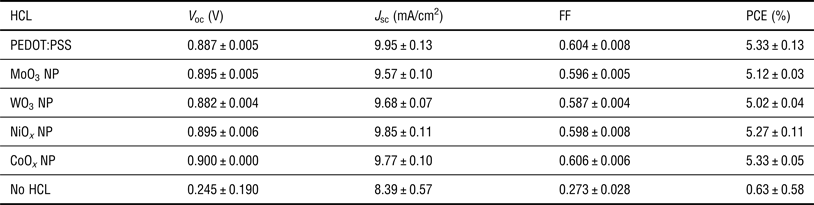
We examined the performance of metal oxide NP films as HCLs using conventional PCDTBT:PC71BM OPVs [Fig. 3(a), inset]. Figure 3(a) shows that all devices with metal oxide NP HCLs perform similarly to references devices with PEDOT:PSS HCL under AM1.5G 100 mW/cm2 illumination. Compared with the device without HCL [Fig. 3(a), purple crosses], the devices with HCL exhibit significantly higher V oc (Table II) due to the larger drift field established between the high Φ HCL and Ca. The devices with HCL also exhibit much smaller SD in V oc and power conversion efficiency PCE (Table II), highlighting the importance of the HCL in creating a uniform electrical contact between the BHJ and the anode. Examining the data in detail, devices with n-type MoO3 NP [Fig. 3(a), red squares] and WO3 NP [Fig. 3(a), orange triangles] HCLs exhibit slightly lower short-circuit current density J sc compared with reference devices [Fig. 3(a), black circles], leading to small reductions in PCE (Table II). In contrast, devices with p-type NiOx NP [Fig. 3(a), green inverted triangles] and CoOx NP [Fig. 3(a), blue diamonds] HCLs exhibit similar J sc and PCE as the reference devices. We also compared poly(3-hexylthiophene):phenyl-C61-butyric acid methyl ester (P3HT:PC61BM) devices with different HCLs and found that performance identical to reference devices can be achieved using MoO3, WO3, and NiOx NP HCLs [Fig. S6(a) and Table S1). We note that to optimize OPV performance, the thickness of WO3, NiOx, and CoOx NP HCLs must be decreased by diluting the NP suspensions to one-fourth of the concentration of the MoO3 NP suspension. This effect can be explained by comparing current density–voltage (J–V) curves of P3HT:PC61BM devices with MoO3 and NiOx NP HCLs of different thicknesses. When MoO3 NP HCL thickness was varied, we found the minimal effect on the J–V curves [Figure S6(b)]. In contrast, when NiOx NP HCL thickness was increased, the J–V curve developed a distinct S-shape, significantly decreasing device FF [Fig. S6(c)]. S-shaped J–V curves have been attributed to inefficient collection of one type of carriers that can be caused by low contact layer conductivity, changes in recombination, or variable electric field distributions, which depends on the specific metal oxide HCL.[Reference Wagenpfahl, Rauh, Binder, Deibel and Dyakonov28] Thus, by optimizing the thicknesses of metal oxide NP HCLs, performance matching PEDOT:PSS is achieved for conventional PCDTBT:PC71BM and P3HT:PC61BM OPVs. Decreasing HCL thickness from the optimal values lowered device yield.
J–V response under AM 1.5 100 mW/cm2 through a 2.5 mm diameter aperture for PCDTBT:PC71BM OPVs with different HCLs. (a) Conventional devices with PEDOT:PSS (black circles), MoO3 NP (red squares), WO3 NP (orange triangles), NiOx NP (green inverted triangles), CoOx NP (blue diamonds), and no HCL (purple crosses). Device parameters are given in Table II. Inset: conventional device architecture. (b) Inverted devices with evaporated MoO3 (black circles), as synthesized MoO3 NP (blue diamonds), and butylphosphonic acid modified MoO3 NP (red squares). Device parameters are given in Table III. Inset: inverted device architecture.
Performance of conventional PCDTBT:PC71BM OPVs with different HCLs under AM1.5G 100 mW/cm2 illumination through a 2.5 mm diameter aperture.
To challenge the processability of our metal oxide NP suspensions, we fabricated inverted PCDTBT:PC71BM OPVs with MoO3 NP film as HCL on top of the active layer [Fig. 3(b), inset]. The PCDTBT:PC71BM BHJ places multiple restrictions on solution-processed overlayers. First, the solvent must wet the organic BHJ and form a uniform film. Second, because the performance of PCDTBT:PC71BM device decreases if heated to >100 °C,[Reference Park, Roy, Beaupre, Cho, Coates, Moon, Moses, Leclerc, Lee and Heeger29] the overlayer should exhibit high Φ with minimal processing. J–V curves under AM1.5G 100 mW/cm2 illumination shows that PCDTBT:PC71BM devices with HCLs formed from as-synthesized MoO3 NPs were shorted [Fig. 3(b), blue diamonds], suggesting poor coverage of the BHJ by the MoO3 NPs. This may be caused by the fact that our NPs are not functionalized with surfactants, and aggregate during spin coating instead of uniformly coating the BHJ. To test this theory, we reacted the MoO3 NP suspension with an equal concentration of butylphosphonic acid, which has been shown to form a self-assembled monolayer on metal oxide surfaces via metal-phosphorus bonds.[Reference Gao, Dickinson, Grozinger, Morin and Reven30] Using HCL of butylphosphonic acid-modified MoO3 NPs, the PCDTBT:PC71BM devices worked well, with similar J sc and slightly lower V oc and FF compared with reference devices with evaporated MoO3 as HCL, resulting in PCE of 3.94% versus 5.07% (Table III). The relative surface coverage of MoO3 NP with and without modifier on PCDTBT:PC71BM was reflected in Φ values from the Kelvin probe. Because the Kelvin probe tip size (mm2) is comparable with the device area, Φ values are a good indication of the presence and coverage of a contact layer on this length scale. Φ of PCDTBT:PC71BM film was 4.23 eV, which increased to 4.97 eV with an evaporated MoO3 film on BHJ. Φ of the as-synthesized MoO3 NP film on BHJ was 4.50 eV, and Φ of the butylphosphonic acid modified MoO3 NP film on BHJ was 4.72 eV. Thus, butylphosphonic acid modification improved the coverage of MoO3 NPs on PCDTBT:PC71BM and increased the collection efficiency for holes, which explains the improvement in FF. We anticipate that further PCE improvements can be achieved by optimizing the functionalization of the NP surface to achieve full coverage on top of BHJ, which is subject to further investigation.
Performance of inverted PCDTBT:PC71BM OPVs with different HCLs under AM1.5G 100 mW/cm2 illumination through a 2.5 mm diameter aperture.
Conclusion
In conclusion, we demonstrate a general method to synthesize stable suspensions of metal oxide NPs using controlled oxidative dissolution of micron-sized metal powders with H2O2 in n-butanol. The small NP diameters of 1–2 nm enable solution processing of n- and p-type metal oxide NP films on ITO with electronic properties comparable with solution-processed and vacuum-deposited counterparts, without the need for any post-processing. Owing to their high Φ values, the metal oxide NP films exhibit excellent performance as HCLs in conventional OPVs, with PCE in most cases identical to the PEDOT:PSS HCL reference. With appropriate functionalization of the MoO3 NP surface to improve film uniformity on top of the organic active layer, performance-approaching evaporated MoO3 HCL was also achieved in inverted OPVs. Owing to the simplicity and generality of the technique, synthesis of other ultrasmall NPs with tailored properties, e.g., ternary/quaternary and doped metal oxide NPs, should be achievable, with potential applications in many areas, such as photovoltaics, thin film transistors, batteries, and catalysis.
Experimental
Metal oxide NP synthesis and characterization
Metal oxide NP suspensions in n-butanol were synthesized using a modified version of a published recipe.[Reference Redel, Huai, Dag, Petrov, O'Brien, Helander, Mlynarski and Ozin21] Mo (average particle size 2–4 µm), W (1–5 µm), Ni (2.2–3.0 µm), and Co (1.6 µm) powders were purchased from Alfar Aesar and were used as received. In a typical reaction, 0.3 mmol metal powder was added to 525 µL n-butanol (Fisher) and 75 µL HCl (37% in H2O, Fisher) and stirred at 25 °C for 20 min. 2220 µL of n-butanol and 180 µL of H2O2 (30% in H2O, Fisher) were then added, and the solution was stirred at 25 °C for 16 h, yielding 0.1 M suspension of metal oxide NPs. The product was passed through a 0.2 µm PTFE syringe filter (Pall), and was used without further purification. DLS was performed using a Malvern ZetaSizer Nano ZS. For TEM, NiOx NP suspension was diluted to 0.005 M with n-butanol, drop casted on a TEM grid (01824, Ted Pella), and imaged at 200 kV with a JEOL JEM2100. NP diameter was analyzed using ImageJ and represents an average of 80 NPs. Metal oxide NP films of different thicknesses were formed by diluting the stock NP suspensions with n-butanol, and spin coating 2–4 layers. For WF and XPS measurements, 0.05 M metal oxide NP suspensions were spin coated twice at 8000 rpm on unpatterned ITO on glass (20 Ω/□, Thin Film Devices) that had been cleaned by rinsing with IPA and H2O, follow by UV-O3 cleaning for 20 min (BioForce Nanosciences). Φ was measured in air using a scanning Kelvin probe (SKP 5050, KP Technology), with Au as the reference material (Φ = 5.15 eV). XPS was measured using a Ulvac-PHI VersaProbe 2 with monochromated Al Kα source (1486.8 eV). All spectra were collected at an angle of 45° to the sample surface with energy step of 0.1 eV and pass energy of 23.5 eV, and were fitted using commercial software (MultiPak, Ulvac-PHI). UPS was measured on MoO3 and WO3 films using the same instrument with He I plasma source (21.2 eV) with energy step of 0.1 eV. PESA was performed on NiOx and CoOx NP films using a RKI Instruments Model AC-2 system with 100 nW deuterium lamp power and energy scanning between 4.8 and 6.2 eV with a step of 0.05 eV. The SD for Φ measurement was found to be 0.03 eV. The uncertainty of the UPS and PESA measurements were found to be 0.1 and 0.05 eV, respectively.
OPVs fabrication and characterization
Conventional and inverted PCDTBT:PC71BM OPVs were fabricated following published procedure[Reference Park, Roy, Beaupre, Cho, Coates, Moon, Moses, Leclerc, Lee and Heeger29] with modifications. For conventional devices, metal oxide NP suspensions (0.025 M for MoO3, 0.00625 M for others) were spin coated four times at 8000 rpm on patterned ITO on glass (20 Ω/□, Thin Film Devices) to form the HCL. For reference devices, PEDOT:PSS (Clevios P VP AI 4083, Heraeus) was mixed with isopropanol in a 7:3 volume ratio, spin coated at 4000 rpm on patterned ITO, and annealed in N2 at 170 °C for 5 min to form the HCL. PCDTBT (1-Material) and PC71BM (Solenne BV) were dissolved at 7:28 mg/mL in ortho-dichlorobenzene (Aldrich), spin coated at 2000 rpm, and annealed in N2 at 70 °C for 15 min to form 50 nm thick BHJ. Finally, Ca (7 nm) and Al (150 nm) were thermally evaporated (Angstrom Engineering) to complete the devices. For inverted devices, ZnO sol–gel film ECL was spin coated on patterned ITO at 5000 rpm from a solution of 0.5 M zinc acetate dihydrate and 0.5 M ethanolamine in 2-methoxyethanol and annealed in air at 170 °C for 10 min, followed by rinsing with H2O, IPA, and acetone. PCDTBT:PC71BM was then spin coated and annealed. For butylphosphonic acid modification of MoO3 NP, equal volumes of 0.1 M MoO3 NP suspension and 0.1 M butylphosphonic acid (Alfar Aesar) were mixed and stirred at 25 °C for 16 h. For HCL, 0.025 M suspension of as synthesized MoO3 NP or butylphosphonic acid modified MoO3 NP was spin coated four times at 8000 rpm on the BHJ. For reference devices, 10 nm MoO3 was thermally evaporated as HCL. Finally, 100 nm Ag was thermally evaporated. The class AAA solar simulator (Sun 3000, Abet Technologies) contained AM1.5G filter, with the intensity adjusted to 100 mW/cm2 using a calibrated Si photodiode with KG5 filter (RR_227 KG5, Abet Technologies). The J–V measurement was performed in N2 using a low-noise sourcemeter (2635A, Keithley) controlled by LabView (National Instruments). A 2.5 mm diameter aperture was placed in front of each device to rigorously define the illumination area to 0.049 cm2. All data shown represent the average of at least five devices.
Supplementary materials
For supplementary material for this article, please visit http://dx.doi.org/10.1557/mrc.2015.5
Acknowledgments
This project was sponsored by National Science Foundation (NSF) DMR-1305893 and University of Texas at Dallas. D.B. acknowledges the support of Consejo Nacional de Ciencia y Tecnología (CONACyT) NL-2010-C33-149216. J.W.P.H. acknowledges the support from Texas Instruments Distinguished Chair in Nanoelectronics.