I. INTRODUCTION
Hard, wear-resistant, and low-friction materials are essential for the present technology and are a key issue in the development of more environmental friendly processes. Friction in mechanical systems is responsible for the waste of enormous amounts of energyReference Nakada1 when considered worldwide, with direct implication in transportation technologies like railwaysReference Clayton2 or automobiles.Reference Tung and McMillan3, Reference Priest and Taylor4 Wear is the key process controlling the lifetime of engines and machinery and is strongly related to the hardness of the pieces in contact. Hard tools are required to machine metals at faster speeds and reduce the use of contaminant cooling and lubricant fluids.Reference Cselle and Barimani5 Based on these premises, the development of hard and lubricant coatings has become a very active research field for the metal transformation and mechanical industries.Reference Kalss, Reiter, Derflinger, Gey and Endrino6, Reference Arnell7 Moreover, hard and lubricant coatings are also a key ingredient of magnetic hard disks, representing a multibillion dollar business.Reference Khurshudov and Waltman8
The compounds of the boron–carbon–nitrogen (B–C–N) system are among the most interesting materials in this area because they exhibit outstanding properties regarding hardness and lubrication.Reference Veprek9 The three hardest materials in bulk form belong to this B–C–N system: diamond, cubic boron nitride (c-BN), and boron carbide (B4C), with hardness values around 100 GPa, 45 GPa, and 35 GPa, respectively. This has motivated intensive research in B–C–N for their application in thin film form and also for the synthesis of new phases within this composition triangle. Bulk compounds of the B–C–N system present commonly one of the three following bonding structures: (i) sp3-based tetrahedral coordination, characteristic of cubic crystals as in diamond or c-BN, (ii) sp2-based trigonal coordination, characteristic of hexagonal crystals as in graphite or h-BN, and (iii) formation of B12 icosahedral units forming rhombohedral crystals as in B4C. These three structures are depicted in Fig. 1.
Possible crystal structures for compounds of the B–C–N system: (a) cubic, (b) hexagonal, and (c) rhombohedral based on B12 icosahedra.

Another source of interest in B–C–N compounds stems from the soft hexagonal phases, like graphite or hexagonal boron nitride, because of the possibility to obtain fullerene and nanotube structures of binary and ternary compounds,Reference Arenal, Blase and Loiseau10–Reference Terrones, Grobert and Terrones12 isoelectronic to their carbon analogues.Reference Terrones13 More recently, the discovery of graphene as a stable one-atom-thick layerReference Geim and Novoselov14 has triggered new interest in the possibilities of attaining B–C–N analogues of graphene.Reference Raidongia, Nag, Hembram, Waghmare, Datta and Rao15, Reference Martins and Chacham16
The synthesis and growth of ternary B–C–N compounds in thin film form can be attained by different physical vapor deposition (PVD) and chemical vapor deposition (CVD) techniques. Among them, ion-beam-assisted deposition (IBAD) is especially powerful for the formation of binary and ternary B–C–N compounds and is discussed in detail in this review.
IBAD consists in the simultaneous thin film deposition and directed ion bombardment.Reference Aisenberg and Chabot17, Reference Aisenberg and Chabot18 The neutral species is normally delivered via PVD by evaporation, ion-beam sputtering, or laser deposition. Evaporated neutrals arrive with their thermal energy, typically 0.1–0.2 eV, whereas sputtered neutrals can arrive with energies of several electron volts. Interaction of the directed ions with the impinging neutrals leads to energy transfer between particles and formation of more or less stable moieties by physicochemical interaction at the substrate surface. In the case of nonreactive IBAD with inert gases like Ar, the main effect is to increase the energy of the neutral atoms by collision with energetic inert ions. In the case of reactive IBAD by using reactive gases like nitrogen or oxygen, one obtains nitrides or oxides of the evaporated metal.
IBAD has been used since the 1970s for the processing of different coating materials, aiming toward the control of the film density, internal stress, texture, and adhesion. There are several review articles that have analyzed these points.Reference Mattox19–Reference Anders25 Initially, the effect of non-reactive IBAD of metals was studied, and how the bombardment conditions affected physical properties like the resistivity, optical transmission, or magnetization that depended mainly on the film density. Later on, metal nitrides (Si3N4 or TiN) and oxides (TiO2) formed by reactive IBAD were studied in detail aiming toward denser and harder coatings.Reference Ensinger24, Reference Zhang and Brodie26, Reference Ma, Huang and Chen27 Since the 1990s, the possibility of controlling the biaxial texture of metal oxide films like MgO, NiO, or yttria-stabilized zirconia by IBAD has attracted great interest for their use as templates for high temperature superconductor thin films.Reference Iijima, Tanabe, Kohno and Ikeno28, Reference Matias, Gibbons and Feldmann29
In this article, we review the use of IBAD to obtain thin films composed of the elements boron, carbon, and nitrogen, including elemental, binary, and ternary BxCyNz compounds. As mentioned above, the interest in this family of materials is double: on the one hand, the hard phases are searched for their tribomechanical properties in applications as protective and lubricant coatings and on the other hand, the hexagonal soft phases are interesting for their use as low-dimensional objects with fullerene-, nanotube-, or graphene-like structures.
II. TECHNICAL CONSIDERATIONS
Here, we will consider the case of boron and carbon evaporation simultaneously to bombardment with a nitrogen ion beam as an ideal situation with all the fluxes of impinging atoms controlled independently with well-defined energies and directionalities. This is not the case in biased magnetron sputtering or arc evaporation, where neither the fluxes nor the energies or the particles are well known, although the ease of up-scaling has made them more common deposition methods for industrial processes.
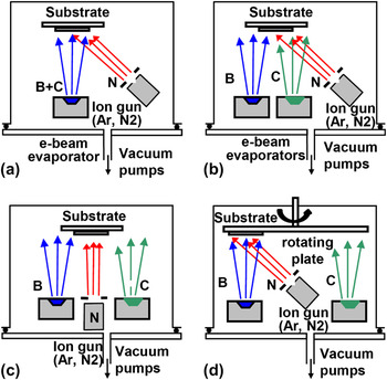
Figure 2 shows a sketch of four geometries used for B–C–N growth, using either a single evaporator filled with pieces of B4C, Fig. 2(a), or two separated evaporators for B and C fluxes, Figs. 2(b)–2(d). For the growth of ternary BxCyNz, the incidence of the nitrogen has to take place at the intersection of the boron and carbon fluxes, as represented in Figs. 2(b) and 2(c). The ion gun can be mounted for oblique or normal ion incidence bombardment. For the growth of C/BN or CNx/B multilayers, the nitrogen ion beam is only coincident with one of the atomic fluxes, either by using the configuration represented in Fig. 2(d) or by using discontinuous fluxes of B, C, and N, controlled by independent shutters.
Sketch of four geometries used for B–C–N growth: (a) single evaporator filled with B4C and oblique ion incidence, (b) independent evaporators for B and C plus oblique ion bombardment, (c) two evap-orators with normal ion bombardment, and (d) ion bombardment concurrent to only one of the atomic fluxes, used for multilayer growth in combination with a rotating sample holder.

A. Evaporation of boron and carbon
The evaporation growth process consists in the transformation of a solid source into a vapor and the subsequent condensation of the vapor on the substrate. Since boron and carbon are refractory materials, resistive evaporators are not suitable. Electron beam evaporation permits high-power densities, of the order of 103 W·cm−2, capable of evaporating any solid. Evaporation takes place in a vacuum, at pressures below 10−5 mbar, and under these conditions the mean free path of the vapor atoms is of tens of meters; hence, they do not collide before condensation on the substrate. The density of atoms in the vapor decreases with the vertical distance, d, from the source as d −2 and with the angle formed with the normal as cosnθ, where the exponent n depends on the details of the evaporation conditions like the area of the source compared to the dimensions of the setup, being either point-like or extensive, the formation of a crater on the source material, the evaporation rate, and so on.Reference Graper30–Reference Aubreton, Bessaudou and Di Bin33 Therefore, it is essential to do a complete characterization of deposition rates from the two sources and their angular dependence.
In the case of carbon evaporation, it may be difficult to maintain a feedback control of evaporation from the readout of a quartz crystal balance due to the high thermal load. If that is the case, a detailed calibration of evaporation rate and its time dependence is required. As evaporation takes place from the source, a crater starts to form and the surface irradiated by the electron beam increases. If the evaporator power is kept constant, the surface power density decreases, as well as the evaporation rate. One needs to compensate for this effect by increasing the evaporator power with deposition time if a constant evaporation rate is desired.
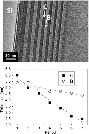
Such an effect is shown in Fig. 3 for the evaporation of a B/C multilayer, where the evaporation power was not changed during the process. Due to the decrease of evaporation rate with time, the thicker layers are located at the interface with the Si substrate.
Boron/carbon multilayer produced by sequential exposure to B and C fluxes, evidencing the decrease of evaporation rate with time for a constant power of the electron beam evaporators.

B. Ion-beam assistance
Ion sources are able to supply a beam of ions, generally positive, accelerated to certain energy within a definite solid angle. They are based on plasma discharges in gases, where positive ions and electrons coexist in approximately the same proportion along with unionized neutrals. The ions from the discharge are extracted from the plasma and accelerated with a specific energy so that they can be directed to a target. The different source types differ in the way the discharge is provoked and sustained (either by direct current or alternating current voltages, generally under the presence of a magnetic field), and also in the extraction and acceleration system for the ions.
The three most common types of ion guns are:
(i) Kaufman sources,Reference Kaufman, Cuomo and Harper34, Reference Harper, Cuomo and Kaufman35 which provide a broad and uniform ion beam in a wide range of energies (100–1200 eV), with extraction grids that can collimate or defocus the ion beam, but suffering from using as cathode an incandescent filament that impedes the use of highly reactive gases like oxygen.
(ii) End–Hall source,Reference Kaufman, Robinson and Seddon36 which is gridless, uses a filament as cathode and provides a divergent broad beam of low energies (up to 200 eV).
(iii) Radiofrequency (RF) ion sourcesReference Keller, Forster and Barnes37 have the advantage of ionizing the gases without the use of incandescent filaments and hence can be used with any gas. They can be constructed with inductive or capacitive coupling of the RF power and different geometries, yielding uniform or divergent beams, with an energy range similar to Kaufman sources.
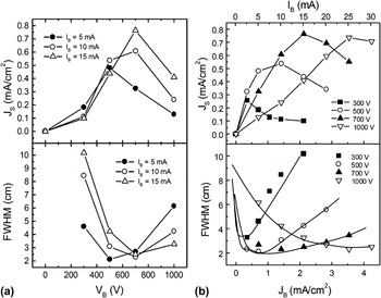
To get a correct measure of the ion flux, it is necessary to measure it at the location of the substrate with a Faraday cup, since the extracted beam current does not match the operating parameters and reading values of the ion source. For the case of a 3-cm-diameter Kaufman ion gun, Fig. 4 shows in the top panels the dependence of the ion–current density measured with a Faraday cup at the sample location, as a function of the ion gun operation parameters beam voltage (V B) and beam current (I B), and in the bottom panels the full width at half maximum of the ion-beam distribution.
Sample current (J s) and width of the ion-beam distribution at full width at half maximum (FWHM) as a function of the (a) beam voltage V B and (b) beam current I B.

III. ION–ATOM INTERACTION
The bombardment of solid targets with energetic particles (10–104 eV) can induce beneficial modifications in the surface and near-surface regions. The use of ion bombardment in the first stages of the deposition can be used to modify the nucleation and growth processes or to improve the film–substrate adhesion. Complementary, properties such as chemical composition, density, hardness, roughness, and structure (grain size, crystalline orientations, intrinsic stress, etc.) can be manipulated by the ion assistance.
The technological relevance of ions is that they can be easily generated, accelerated, and filtered. The effects induced upon ion bombardment depend strongly on the ion energy and mass. According to the kinetic energy, the ions can be referred as “thermal” (<1 eV), “hyperthermal” (1–1000 eV), “low energy” (1–10 keV), “medium energy” (10–500 keV), and “high energy” (>0.5 MeV).
The hyperthermal range is typical of IBAD processes, where the relevant effects are ballistic, i.e., the accelerated ions have enough energy to induce bond breaking and relocation processes in the atomic lattice. The collision or knock-on processes between the incident ion and the rest atoms induce “atom displacements” in the solid. The energy transferred to the rest atom in the collision should be high enough to overcome the so-called “displacement energy.” These energies are typically around 10 eV and are proportional to the binding energy of the atom in the solid. In the simplest case, the displaced atom leaves a vacancy and occupies an interstitial position. This vacancy–interstitial defect is referred as a “Frenkel pair.” For increasing energies above the displacement threshold, the primary knock-on atom can also displace other atoms of the network, creating a “collision cascade.”
A. Ballistic model and relevant ion assistance parameters
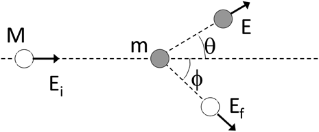
As energetic particles or ions travel through the solid, they interact with the atoms of the target. In a simple approximation, we can consider a binary collision between a fast moving particle with an atom at rest in its lattice position, as is displayed schematically in Fig. 5. In the energy range for ion-assisted processes (below a few kiloelectron volts), the typical penetration depth is of a few nanometers. Therefore, the time scale for a particle in this energy range to be stopped within the solid is of ∼10−13 s. This time scale is of the same order as that for lattice vibrations and, therefore, the description of the ion bombardment considering a binary collision between a fast moving particle and a rest atom is justified.
Binary collision between an incoming particle (M) with energy E i and an atom at rest (m).
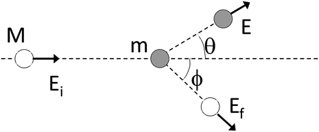
Assuming an elastic collision, the energy conferred from the incoming ion to the atom at rest is the “transfer energy,” E:

where φ represents the scattering angle as displayed in Fig. 5. The ratio between E and E i, k, is known as the “kinematic factor,” which has a maximum value (k = 1) for a head-on collision (φ = 0) and when M = m. In other cases, the kinematic factor will be always below 1.
The “momentum transfer” in the collision, ΔP, is

An important parameter for the quantification of the ion bombardment during film growth is the “transport ratio,” T = I/A, which corresponds to the arrival ratio of incoming ions and neutral atoms:
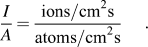
This term acts as a normalization factor of the bombardment parameters to the rate of material deposition. Typical values of the transport ratio in ion assistance processes range between 0.1 and 5.
The effects of the ion energy on the film growth can be normalized by introducing the “average energy deposited” per incoming ion, E d, which can be easily calculated as:
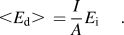
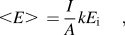
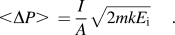
The E d value has been recognized as a relevant parameter for describing the effects of low-energy (about 100 eV) ion irradiation, but it cannot be used as a universal parameter.Reference Petrov, Adibi, Greene, Hultman and Sundgren38 A more precise description should incorporate the kinetics of the collision process. In this way, the “average transfer energy,” <E>, and the “average momentum transfer” per incoming ion, <ΔP>, must be introduced to account for the quantification of the ion bombardment:
In the case of assistance with several ion species, the above expressions can be expanded as the sum of the individual terms, corresponding to each species.Reference Kester and Messier39
The above equations assume that the collisions are binary and elastic. This is only an approach for the quantification of the ion bombardment since many-body collisions have to be considered in a real case. As a final remark, when looking at the effects of ion bombardment, the ion energy and the transport ratio effects should not be considered separately. The resulting modifications at a given transport ratio may vary depending on the energy of the ions and, likewise, the effect of bombardment at a given ion energy will also depend on the number of bombarding ions.
B. Influence of ion bombardment on film properties
From the materials science and technology standpoints, the interest in using ion-assisted deposition stems from the new or enhanced properties that are conferred to the growing films due to the structural changes induced by the ion irradiation.
To predict the influence of ion bombardment on the film properties, three main theoretical approaches have been followed. The first one is the “thermal spike” continuum modelReference Trinkaus40, Reference Hofsass, Feldermann, Merk, Sebastian and Ronning41 based on assuming that the local energy deposited in the collision cascades relaxes in a very short time (typically 1 ps) giving rise to a high local temperature, well beyond the melting point of any solid, for a very short time and limited to the volume surrounding the ion tracks. The second one is the “ballistic or collision-cascade” model.Reference Miotello and Kelly42 This is a discrete model based on accounting for the atomic displacements induced by the energetic ions due to the transfer of energy and momentum in the collision. In many cases, a simple version of the ballistic model is considered by using ion implantation models, like the TRIM code,Reference Biersack and Haggmark43 where the ions reach a preformed material and not a growing film. The third model is based on “molecular dynamic” calculations, an atomistic model that accounts for the impingement of both atoms and hyperthermal ions and the interactions among them.Reference Caturla, delaRubia, Marques and Gilmer44 The accuracy of their predictions largely remains on the description of the interaction potentials between particles.
The ion bombardment induces three main types of effects on the film growth that are summarized below.
1. Ion-induced modifications of the film microstructure
a. Grain size
The energetic ions influence the balance between nucleation and growth by increasing the surface mobility of atoms, creating defects that act as nucleation sites, sputtering away of the smallest islands, and disrupting the columnar growth of tall grains. The balance between these four processes finally controls the result, which depends on the ion energy and transport ratio and is specific of each system.Reference Durand, Sekine, Etoh, Ito and Kataoka45 In general, there is a decrease in grain size with ion bombardment for low energies (10–100 eV). The grain size increases for energies exceeding 10 keV due to recrystallization of the film by the thermal spike associated with the high-energy ions.Reference Mayr and Averback46
b. Surface and interface roughness
In principle, a smaller grain size yields a lower roughness. Additionally, some textures or crystal orientations yield smoother surfaces than others. In general, when the more densely packed crystallographic planes are parallel to the surface, the roughness decreases.Reference Ji and Was47 The final roughness is due to the balance between thermodynamics, that tends to create smooth surfaces by arranging all atoms in the position of maximum coordination, and kinetics, that tends to stick the arriving particles in random positions. In general, there is a decrease in surface roughness for low ion-beam energies (50–100 eV), followed by a small increase for energies beyond this range. The same applies to the interface roughness during the growth of multilayer coating.Reference Telling, Guilfoyle, Lovett, Tang, Crapper and Petty48
c. Film density
The films produced by IBAD are normally denser than those produced by thermal evaporation, due to the capability of the hyperthermal particles to disrupt the columnar growth, preventing voids between the columns. The void fraction decreases with the transport ratio and energy of the ions until a maximum density is obtained for the optimal values of energy and I/A ratio. Beyond the optimal values, which are around 50 eV, there is an increasing damage in the films with crystallographic defect formation that decreases the density.
A second process affecting the film density is the denser packing of atoms in the films due to both the shortening of bonding distances and the increasing number of atoms in interstitial positions, effects that also yield an internal compressive stress.
d. Defect generation
Ion irradiation of solids creates a large number of vacancies, interstitials, and dislocations by atomic displacements, although the thermal spike associated with the ion irradiation can also anneal out many of them.
A type of defects specific of ion assistance is the incorporation of atoms or molecules that were present as ions in the bombarding beam. Inert atoms like Ar or molecules like N2 have been found embedded in the films grown by ion assistance, with typical concentrations of 1–5 at.%.
e. Internal stress
Thin films grown by PVD methods can accumulate an internal stress during growth that increases with the film thickness, being a limiting factor for possible applications.Reference Windischmann49 When the internal stress exceeds a critical value, the films delaminate. The stress is referred as “tensile” when it increases the length of a solid and is assigned a positive value. In the case of thin films, tensile stress corresponds to an in-plane enlargement. The stress is “compressive” when it shortens the solid, taking a negative value, and in films it corresponds to an in-plane shrinkage. A large void fraction in the film induces a tensile stress since such a low-density film is actually occupying more volume that would correspond to the number of atoms present in the film. On the contrary, a high-density film containing a large proportion of interstitial atoms presents compressive stress.
For IBAD films grown with very low-energy ions, typically below 1 eV, the adatom mobility is enhanced without disrupting the columnar growth and this results in a slight increase of the tensile stresses due to a larger size of the voids. More energetic ions disrupt the columnar growth, releasing the tensile stress associated to the voids. IBAD at ion energies of about 1–50 eV normally results in compressive stress since the atomic packing increases with the ion bombardment by occupation of interstitial positions.Reference Windischmann50, Reference Windischmann51 Finally, for more energetic ions, the thermal spike releases the compressive stress and the film densification.Reference Davis52 Based on these facts, the use of ion assistance permits the control of the film internal stress from a positive stress in the case of non-ion-assisted films to a compressive stress in IBAD films.Reference Pauleau53, Reference Dheurle and Harper54
f. Film texture
Normally, the films obtained by deposition without energetic ions present the most densely packed planes parallel to the surface since the arriving particles tend to bond in a configuration of maximum coordination. However, under ion bombardment, the closest packed planes tend to move out of this geometry with new textures in the filmsReference Shin, Cho, Won, Kang, Baeg, Hong and Wey55 due to compressive stress and preferential sputtering of such highly packed structures during growth. The compressive stress that is built up during IBAD tends to orient the planes with the lowest in-plane compressibility, i.e. the closest packed ones, perpendicular to the surface. A clear example occurs in the IBAD growth of highly anisotropic layered materials, like hexagonal boron nitride, where the compressive stress tends to orient the basal planes perpendicular to the surface, even in films lacking long-range order. The “preferential sputtering model” assumes that the arriving ions find a well-defined crystalline structure, with more or less open channels in the direction of motion depending on the grain orientation. If the texture is not closed packed, the channels are wider and the ions can penetrate deeper in the bulk without collisions. However, for closed-packed structures the channels are narrow and the ions collide near the surface producing sputtering and removal of the closed-packed planes.Reference Dong and Srolovitz56
2. Ion-induced modifications of the bonding structure
a. Amorphization
To define a true amorphous material, it is necessary to express the extent of the local order. A material maintaining the coordination number and bonding distances of the crystalline reference, but exhibiting different bonding angles beyond the second nearest neighbor coordination sphere, would have a well-defined bonding structure similar to the crystalline reference, but without any long-range order. This is, for instance, the case of amorphous SiO2. A more extreme amorphous material occurs even when the coordination number is not similar to any crystalline reference, and hence the bonding distances and angles are not maintained. This situation occurs in amorphous or diamond-like carbon (DLC), where different bonding mixtures between trigonal sp2 hybrids and tetragonal sp3 hybrids takes place, unlike the reference single hybrid configuration of graphite and diamond crystalline materials.
Ion assistance affects the crystallinity of the material, and a significant broadening of the Bragg reflections or even the loss of the Bragg peaks, due to ion-induced disorder in the structure, can be found with increasing bombardment (both by ion energy and transport ratio). However, beyond a certain point, the thermal spike produced by ion assistance counteracts this effect, leading to film recrystallization.
b. Stabilization of metastable phases
Nowadays, one of the main applications of deposition techniques far from thermodynamic equilibrium, like IBAD, is the stabilization of certain phases at growth temperatures well below the phase transition or even the synthesis of films in a metastable phase not achievable by techniques under thermodynamic equilibrium conditions. One example of phase stabilization is the case of TiO2 that grows in the anatase phase for T<600 °C and in the rutile phase for T>600 °C. However, by IBAD techniques, the rutile phase can be grown at temperatures below 600 °C.Reference Lobl, Huppertz and Mergel57 Regarding the synthesis of metastable phases, some examples are the growth of diamond-like films with tetrahedral coordination (ta-C), cubic BN (c-BN), or cubic GaN (c-GaN), instead of the more stable phases graphite, h-BN, and wurzite GaN, respectively. The binding energy difference between w-GaN and c-GaN is only 0.2 eV; therefore, the transfer of energy and momentum to promote the synthesis of c-GaN is not difficult and can be achieved by a nitrogen plasma without additional ion acceleration.Reference Okumura, Ohta, Feuillet, Balakrishnan, Chichibu, Hamaguchi, Hacke and Yoshida58 However, the binding energy difference for carbon or BN in sp3 and sp2 coordination is very large, of the order or 1 eV, and the growth conditions to obtain the sp3 phases are rather stringent.
In the case of ta-C, the use of a monoenergetic beam of carbon atoms of about 100 eV is required while maintaining the substrate at room temperature.Reference Chhowalla, Robertson, Chen, Silva, Davis, Amaratunga and Milne59 In this case, the conventional IBAD setup with Ar+ assistance is not optimal since it provides a broad range of energies to the carbon atoms. Instead, the filtered cathodic vacuum arc (FCVA) technique is used, where a plasma of carbon is produced by arc evaporation and the mass is filtered so that only carbon with the optimal energy of about 100 eV bombard the substrate by biasing the substrate.Reference Fallon, Veerasamy, Davis, Robertson, Amaratunga, Milne and Koskinen60 In the case of c-BN, conventional IBAD with the assistance of argon and nitrogen ions is a well-suited technique, comprising the optimal conditions of a transport ratio about unity, ion energy of about 500 eV, and a substrate temperature near 500 °C.
The mechanism permitting the synthesis of metastable phases is based on a local increase of temperature and pressure due to the ion bombardment that mimics the macroscopic conditions obtained in the high temperature high pressure (HTHP) synthesis of such materials from starting powders. The most accepted theoretical model accounting for such phase transformation is the subplantation model, where energetic particles in the subsurface attain locally the conditions for the sp3 phase stabilization.Reference Lifshitz, Kasi, Rabalais and Eckstein61, Reference Robertson62
3. Ion-induced chemical effects
When non-reactive ions are used, mainly Ar+ and Ne+, the formation of the compound takes place by chemical reaction between the different atomic species evaporated or sputter deposited. The impinging ions play a double role: (i) they communicate energy and momentum to the neutral atoms or molecular moieties arriving at the substrate surface, favoring the chemical reactivity and (ii) they modify the composition due to the preferential sputtering of a certain chemical element compared to another, an effect that is energy dependent. Also, there is a small incorporation, typically of 1–5%, of the neutralized ions in the film.
The use of reactive ions, normally oxygen or nitrogen, is a common method of forming thin films of oxides (SiO2, PbOx, CuOx MgO, ITO, etc.) and nitrides (TiN, AlN, GaN Si3N4). In this case, the reactive ions can react with the neutral atoms yielding stable compounds that are incorporated to the film or they can form volatile moieties that are desorbed from the substrate, producing the so-called chemical sputtering. This latter process consumes part of the evaporated atoms and should be minimized to make the IBAD technique efficient. All these effects are also dependent on the ion energy, and normally there is an optimal value for the formation of stable moieties that incorporate to the film. The amount of reactive gas that is incorporated to the film depends linearly on the actual supply of reactive gases, i.e., on the ion/atom ratio, until a saturation level is obtained. The saturation is obtained for I/A values below the compound stoichiometry, indicating that not all the evaporated atoms incorporate to the film due to chemical sputtering. For I/A values above the saturation point, chemical sputtering is enhanced, reducing the growth rate.
The stabilization of compounds with unusual composition or stoichiometry, e.g., subnitrides or supernitrides with a coordination number larger than the common phase, can also take place in the IBAD film growth, a mechanism that can be considered as the stabilization of metastable phases from the chemical point of view, in contrast with the geometrical metastable phases considered in the preceding section.
IV. IBAD OF ELEMENTAL AND BINARY B–C–N MATERIALS
A. Carbon films: Diamond and DLC
The growth of carbon films with energetic particles has been aimed toward the synthesis of amorphous hard carbon coatings, such material normally referred as diamond like carbon (DLC),Reference Robertson63 which despite being softer than diamond has very interesting physical properties. Crystalline diamond thin films are not obtained by IBAD, but by CVD methods using mixtures of a carbon precursor gas (CH4, C2H2, …) and a large concentration of hydrogen. The gas molecules are activated by plasmas or hot filaments to produce atomic hydrogen which etches preferentially graphite and stabilizes the sp3 phase of carbon.Reference Yarbrough and Messier64 In addition, a high substrate temperature is required. Bombardment with energetic particles is only relevant at the initial nucleation stage, since formation of diamond nuclei is largely activated when a bias voltage is applied to the substrate in the so-called bias-enhanced nucleation.Reference Stoner, Ma, Wolter and Glass65, Reference Garcia, Jimenez, Vazquez, Gomez-Aleixandre, Albella, Sanchez, Terminello and Himpsel66 Several models and mechanisms have been proposed to explain this effect activated by energetic particles.Reference Robertson, Gerber, Sattel, Weiler, Jung and Ehrhardt67–Reference Li, Marks, Lifshitz, Lee and Bello69
With regards to DLC, it comprises actually four different types of materials: (i) tetrahedral amorphous carbon (ta-C), a hydrogen-free material containing a large fraction of sp3 (above 50%) carbon atoms being very hard and lubricant; (ii) amorphous carbon (a-C), a hydrogen-free carbon with a moderate amount of sp3 hybrids (below 50%), and their partially hydrogenated counterparts (iii) tetrahedral amorphous hydrogenated carbon (ta-C:H), and (iv) amorphous hydrogenated carbon (a-C:H). The hydrogenated carbon films are normally obtained by plasma CVD methods, whereas the H-free carbon films require the use of PVD methods with energetic particles.
As commented, the synthesis of ta-C requires the use of filtered carbon particles, which are obtained by FCVAReference Lossy, Pappas, Roy and Cuomo70 and are accelerated to the optimal energy for sp3 promotion, around 100 eV, by applying a bias voltage to the substrateReference Chhowalla, Robertson, Chen, Silva, Davis, Amaratunga and Milne59 or by other techniques with well-controlled ion energies like mass selected ion-beam deposition.Reference Prawer, Nugent, Lifshitz, Lempert, Grossman, Kulik, Avigal and Kalish71, Reference Lifshitz, Lempert, Grossman, Avigal, Uzansaguy, Kalish, Kulik, Marton and Rabalais72
H-free carbon coatings can be obtained by IBAD using coincident beams of neutral carbon atoms and energetic inert ions (normally Ar+) that provide the energy and momentum transfer in the Ar–carbon collisions taking place at the substrate surface. The neutral atoms can be obtained by thermal evaporation, laser deposition, or sputtering from a carbon target.Reference Funada, Awazu, Shimamura, Watanabe and Iwaki73, Reference Sjostrom, Hultman, Sundgren, Hainsworth, Page and Theunissen74 Under these conditions, ta-C is not obtained but a-C films denser than plain evaporated carbonReference Gago, Jimenez, Albella, Climent-Font, Caceres, Vergara, Banks, Doyle and Terminello75 and with good mechanicalReference Funada, Awazu, Yasui and Sugita76, Reference Jun, Luo, Wen, Wang and Li77 and opticalReference Chen, Yu, Zhao, Ren, Ding, Shi and Liu78 properties are formed. These coatings have also applications as biomaterialsReference Cui and Luo79 and can be even grown on plastic substrates.Reference Li, Cui and Gu80 The use of ion bombardment helps to form an adhesion layer with metallic substrates, increasing the adhesion strength.Reference Funada, Awazu, Yasui and Sugita81 Similar coatings can be obtained by biased magnetron sputtering. To obtain partially hydrogenated coatings by IBAD, a common method is to feed the ion gun with hydrocarbon gases like methane to produce CHx+ ions that directly impinge the growing films.Reference Wang, Li and Li82
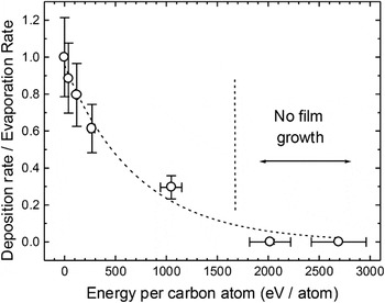
In principle, in IBAD of carbon with concurrent energetic Ar ions, one could increase the energy of the carbon atoms by increasing the energy of the bombarding ions and also the I/A transport ratio, since the latter affects the probability of Ar–carbon collisions. However, the deposition rate decreases rapidly due to resputtering processes. For very high transport ratios of about 10, it is even possible to obtain ta-C by magnetron sputtering,Reference Schwan, Ulrich, Roth, Ehrhardt, Silva, Robertson, Samlenski and Brenn83 at the expense of extremely low deposition rates. Figure 6 shows the decrease of the deposition rate relative to the evaporation rate for carbon evaporation assisted with Ar+ ions.
Deposition rate normalized to the evaporation rate, as a function of the ion energy per carbon atom during deposition. Adapted from Ref. Reference Gago, Jimenez, Albella, Climent-Font, Caceres, Vergara, Banks, Doyle and Terminello75.

For intermediate values of the energy per carbon atom, which is the common situation in IBAD of carbon, one obtains coatings with densities of 2.2–2.4 g/cm3 and hardness of 20 GPa, compared to 1.7–1.9 g/cm3 and 7 GPa of plain evaporated carbon.
Regarding the bonding structure of these IBAD carbon coatings, some authors have described them as an sp2 network with a high compressive stress of 10–15 GPa, where C implantation compacts the structure by reducing the distance between graphitic planesReference Lacerda, Hammer, Freire, Alvarez and Marques84 without evidence of sp3 hybridization. However, studies of the local structure by x-ray absorption near-edge spectroscopy (XANES) indicate a clear decrease in the density of π* states, consistent with a moderate sp3 content up to 25%.Reference Gago, Jimenez, Albella, Climent-Font, Caceres, Vergara, Banks, Doyle and Terminello75 Moreover, in this case, there is no preferential orientation of basal planes, as could be expected for graphite-like planes in compressive stress situation, as is observed in other stressed carbon systems.Reference Jimenez, Garcia, Albella and Terminello85 A detailed XANES study indicates the formation of multiple types of bonding arrangements between sp2 and sp3 hybrids.Reference Jimenez, Gago and Albella86 This is different from a pure ta-C, where the amorphous network is more homogeneous in bonding structure.Reference Gago, Vinnichenko, Jager, Belov, Jimenez, Huang, Sun and Maitz87 These IBAD carbons contain several defectsReference Britton, Harting, Hempel, Gxawu and Uhlmann88 like dangling bonds and paramagnetic defects,Reference Viana, Lacerda, Freire and Marques89 as well as trapped Ar atoms from the bombardment.Reference Lacerda, Hammer, Alvarez and Marques90 There are attempts to describe the structure based on molecular dynamics simulations.Reference Li, Pan, Wang, Wei, Zang, Ye, Bai, Wang and Liu91
Recent work on carbon IBAD is exploring the advantage of the independent control of ion energy and directionality,Reference Sun, Yu, Du and Xue92 in particular, the incidence at oblique angles.Reference Kai, Li, Guo, Li and Li93
B. Boron films
Boron films can be obtained by boron evaporation, boron sputtering,Reference Makowiecki, Jankowski, McKernan and Foreman94 or boron direct ion beams and are in general amorphous. Boron can present α-rhombohedral, β-rhombohedral, and tetragonal crystalline forms based on the arrangement of B12 icosahedra, hence with a similar local structure,Reference Krishnan, Ansell, Felten, Volin and Price95 as shown in Fig. 1(c). Therefore, drastic changes in the bonding structure, density, and film properties are not expected with ion assistance, as occurred for carbon. The only effect of ion bombardment is the build up of internal stress with ion bombardment.Reference Barth, Ensinger, Hoffmann and Wolf96 However, this is an important factor for large-area depositions. One of the main technological interests of boron deposition is the conditioning with low-Z elements of the interior of nuclear fusion reactors to reduce the nuclear plasma poisoning.Reference Winter97 In this sense, there are various studies on the effect of ion irradiation in internal stressReference Satomi, Sato, Tanaka, Saidoh and Nishikawa98–Reference Kemi, Sasaki, Kitamura, Satomi, Ueda and Nishikawa100 and attempts to reduce it using pulsed ion techniques.Reference Audronis, Kelly, Leyland and Matthews101
C. Boron nitride films: c-BN, h-BN, and BNx
Boron nitride films can be grown by reactive IBAD combining the evaporation of boron with nitrogen ion bombardment, or with an ion beam containing both nitrogen and inert-gas ions to provide different values of the average ion mass and momentum. Boron nitride (BN) can be found in sp2 bonding configuration like the hexagonal (h-BN) and rhombohedral (r-BN) forms or in sp3 configurations like cubic (c-BN) and wurzite (w-BN) phases.Reference Terminello, Chaiken, Lapianosmith, Doll and Sato102 Normally, in the analysis of bonding structures, one considers only the most common h-BN as c-BN phases, which are the analogues of graphite and diamond. Therefore, as discussed for carbon growth, the use of energetic particles can promote the formation of the most interesting c-BN, which is a promising candidate as an alternative to diamond in microelectronic and mechanical applications. It is the second hardest material presently known in bulk form, does not react with metals (relevant for coating applications on tools), presents higher thermal stability (up to 1000 °C), and can be either p- or n-type doped.
Most of the work on IBAD of BN has been focused on the synthesis of the cubic phase,Reference Mirkarimi, McCarty and Medlin103 which can be achieved within certain parameters window.Reference Kester and Messier39, Reference Hofsass, Feldermann, Sebastian and Ronning104, Reference Kulisch and Ulrich105 Unlike the case of sp3-bonded ta-C, IBAD is a suitable technique to obtain the sp3 phase of BN. It seems that stabilization of the cubic phase is easier for BN compared to carbon due to the polarity of the BN bonds.Reference Robertson106 The momentum transfer per incoming atom has been shown to be the controlling factor for the final phase configuration (see Sec. III.A). Normally, assistance with only nitrogen ions does not result in c-BN growth, since the momentum transfer is not enough for promotion of the sp3 phase and mixtures of N2 and a heavier noble gas like Ar are required. Typical conditions for c-BN growth are: mixture 50%/50% of N2/Ar in the bombarding gas, ion energies around 500 eV, and substrate temperatures around 500 °C. Under special conditions other parameters may be used, e.g., growth of c-BN can be done at room temperature on substrates with previously formed c-BN nuclei.Reference Feldermann, Merk, Hofsass, Ronning and Zheleva107
As an example, Fig. 7 shows the resulting phase, as derived from infrared (IR) spectroscopy, for BN films grown by IBAD at different substrate temperatures. The cubic content can be derived from the relative intensity of the corresponding h-BN (∼1400 cm−1) and c-BN (∼1100 cm−1) IR absorption bands.
Infrared spectra of boron nitride (BN) samples grown by ion-beam-assisted deposition (IBAD) at different substrate temperatures and constant ion energy of 500 eV.

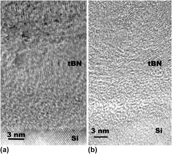
The need of energetic ion bombardment seems to be related to the build up of compressive stressReference Davis52 and formation of defects.Reference Jimenez, Jankowski, Terminello, Sutherland, Carlisle, Doll, Tong, Shuh and Himpsel108–Reference Caretti and Jimenez110 In the most studied case of growth on Si substrates, the cubic phase grows on top of an intermediate buffer layer of hexagonal or turbostratic BNReference Kester, Ailey, Lichtenwalner and Davis111, Reference Yamashita, Kuroda, Saka, Yamashita, Watanabe and Wada112 with the basal planes oriented perpendicular to the surface due to the high compressive stress and which serves as adhesive layer. The thickness of the oriented h-BN layer depends on the growth conditions and, normally, it is of the order of 10–30 nm,Reference Zhang, Boyen, Yin, Ziemann and Banhart113, Reference Djouadi, Vasin, Nouveau, Angleraud and Tessier114 depending on the growth conditions.Reference Li, Marks, Lifshitz, Lee and Bello69 Formation of abrupt interfaces without the h-BN buffer layer have been claimedReference Doll, Sell, Taylor and Clarke115 but are not commonly found. Figure 8 shows a typical high-resolution TEM image of this transition layer.
Transmission electron microscopy (TEM) of the initial stages of BN on Si, with different transition hexagonal-like layers (from Ref. Reference Li, Marks, Lifshitz, Lee and Bello69).

The main problem with c-BN coatings is the high internal stress generated, up to 10–20 GPa, that delaminates films thicker than a few hundred nanometers. Stress buildup is so largeReference Klett, Freudenstein, Plass and Kulisch116 that it can be even detected in the shape of the density of electronic states by XANES.Reference Gago, Abendroth, Cerda, Jimenez and Moller117 This fact has precluded the actual application of c-BN despite its outstanding properties. The formation of layers about 0.7-μm thickReference Mirkarimi, Medlin, McCarty, Dibble, Clift, Knapp and Barbour118 and 2-μm thick have been milestones in the research effort.Reference Yamamoto, Keunecke and Bewilogua119 Therefore, many current attempts are focused on the development of mechanisms for stress relaxation.
The generation of stress by ion bombardment during growth in c-BN fits well with the predictions of Davis’sReference Davis52 model. In this case, the state of compressive stress should be maximum for the ion energies involved in the growth of c-BN (100–500 eV). According to Davis’s model, the stress value could be reduced by increasing the ion energy above this range (∼1 keV); however, this results in a decrease of the growth rate or complete resputtering of the film. Another approach to reduce the stress considers the different parameters window for nucleation and growth, so the requirements for subsequent growth are gentler than for nucleation such as lower substrate temperatures (>100 °C) and lower ion energy (>100 eV).Reference Kulisch and Ulrich105 However, the level of intrinsic stress released in this case is still not sufficient for practical applications.
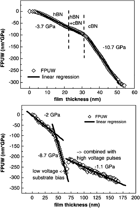
Recently, the use of postdeposition treatments like ion implantation (10–500 keV) and thermal annealing (up to 900 °C) has shown effective results.Reference Widmayer, Ziemann, Ulrich and Ehrhardt120, Reference Ullmann, Kellock and Baglin121 Therefore, the incorporation of these methods in a sequential or simultaneous process during the growthReference Fitz, Fukarek, Kolitsch and Moller122 are the most promising alternatives for the growth of thick c-BN films. However, there are still other issues to be addressed such as the reduction of stress at the interfaceReference Abendroth, Gago, Kolitsch and Moller123 and, in this way, improving the adhesion of a stress-free c-BN layers to the film structure.
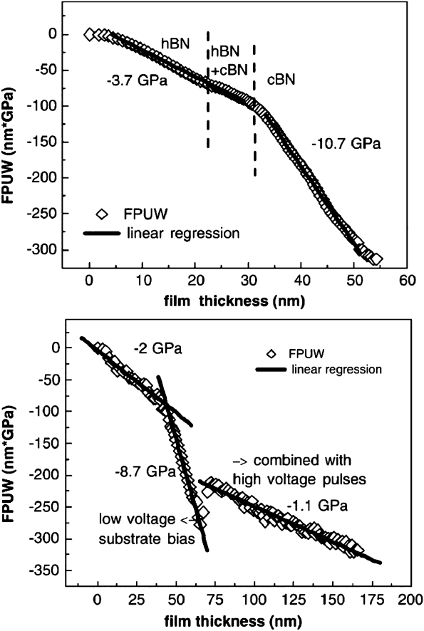
As an example, Fig. 9 shows the film force per unit width measured in situ with a laser deflection system, during magnetron sputtering c-BN growth (top panel), and with a pulsed high voltage cycle added to release the stress (bottom panel).
In-situ measurements of stress buildup during conventional IBAD c-BN growth (top panel) and with a superimposed high voltage cycle. Adapted from Ref. Reference Abendroth, Gago, Kolitsch and Moller123.
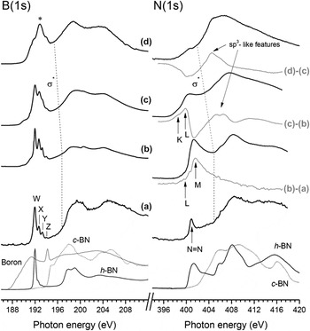
A different research scenario regards the formation of nonstoichiometric BN, ranging from boron rich (subnitrides) to nitrogen rich (supernitrides), a field scarcely explored due to the difficulties to obtain bulk compounds.Reference Solozhenko and Kurakevych124 However, the growth of those materials in thin film form by IBAD is relatively easy by adjusting the boron and nitrogen fluxes. Recent work has shown the variety of bonding structures that can be obtained by IBAD within this B–N system.Reference Caretti and Jimenez125Figure 10 shows the XANES spectra of a number of nonstoichiometric boron nitrides.
B and N K-edge x-ray absorption near-edge spectroscopy (XANES) spectra of samples (a) to (d) with B/(B + N) = 0.41, 0.52, 0.60, and 0.77. Boron, h-BN, and c-BN references are included at the bottom. From Ref. Reference Caretti and Jimenez125.

D. Boron carbide films: B4C and BCx
B4C is the third hardest material presently known in bulk form, with a hardness of about 35 GPa. It exhibits a rhombohedral crystalline structure with distorted B11C icosahedra located at the nodes of the Bravais lattice plus a linear C–B–C chain at the axis of the icosahedra.Reference Lazzari, Vast, Besson, Baroni and Dal Corso126 The structure resembles that of elemental boron and of many boron-rich solids, as shown in Fig. 1(c).
Boron carbide films are normally obtained by thermal evaporation or by magnetron sputtering of B4C targets.Reference McKernan127, Reference Pascual, Martinez, Esteve and Lousa128 However, the compositionReference Caretti, Fanegas, Martin, Torres and Jimenez129 and structure of the film differ slightly from the target.Reference Bao and Chrisey130 Other possible methods of synthesis in thin film form are the reaction of B and C ion beamsReference Todorov, Marton, Boyd, Albayati and Rabalais131, Reference Ronning, Schwen, Eyhusen, Vetter and Hofsass132 or B and C atomic fluxes.Reference Caretti, Gago, Albella and Jimenez133
Under intensive Ar ion bombardment, BCx films build up internal stresses that induce a hardness up to 72 GPa, which is double than the hardness of the bulk material,Reference Widmayer, Ziemann, Ulrich and Ehrhardt120, Reference Ulrich, Ehrhardt, Schwan, Samlenski and Brenn134 although detrimental for film stability as was described earlier for c-BN. Ar ion bombardment during growth also induces a decrease of the deposition rate with the ion energy,Reference Reigada, Prioli, Jacobsohn and Freire135 indicative of physical and chemical sputtering due to formation of BCx moieties, but a minor effect on the coating density, since there is no phase transitions related to densification of the film, as was the case in carbon and boron nitride films. The modifications of internal stress reflect on all the mechanical properties.Reference Kulikovsky, Vorlicek, Bohac, Ctvrtlik, Stranyanek, Dejneka and Jastrabik136, Reference Zhou, Wong, Ong and Li137
Phase changes in BCx films grown by IBAD are associated to composition changes from a B-rich carbide, with the icosahedral units shown in Fig. 1(c), to a hexagonal-like carbon-rich boride.Reference Yanagisawa, Tanaka, Ishida, Matsue, Rokuta, Otani and Oshima138 Also, for carbon-rich borides, cubic phases can be obtained by HTHP methods,Reference Solozhenko, Kurakevych, Andrault, Le Godec and Mezouar139 although there are no reports on their thin film synthesis. Since IR is not very sensitive to the BCx features, other spectroscopies like x-ray photoemissionReference Jacobsohn, Schulze, da Costa and Nastasi140, Reference Bao and Chrisey141 or XANES are considered in this case.Reference Jimenez, Sutherland, van Buuren, Carlisle, Terminello and Himpsel142, Reference Jimenez, Terminello, Himpsel, Grush and Callcott143 As an example, Fig. 11 shows the XANES spectra corresponding to the transition from a B-rich carbide to a hexagonal C-rich boride obtained by selecting the atomic fluxes of the precursors.
XANES spectra showing the transition from a B-rich carbide to a hexagonal C-rich boride obtained by selecting the B/C atomic fluxes. The numbers indicate the C at.% in the films. Adapted from Ref. Reference Caretti, Gago, Albella and Jimenez133.

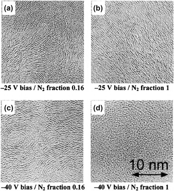
TEM micrographs of CNx films from samples deposited by magnetron sputtering with different N2 gas fractions and bias voltages. Adapted from Ref. Reference Neidhardt, Czigany, Brunell and Hultman170.

E. Carbon nitride films: CNx
The synthesis of carbon nitride (CNx) by IBAD using carbon atoms and nitrogen ions represents a clear example of reactive IBAD using chemical species with low reactivity between them. Therefore, chemical sputtering is a very competitive process with the film growth as will be shown below.
The research on carbon nitrides was very active in the 1990s and 2000s, triggered by some theoretical predictions of a stable β-C3N4 phase with outstanding properties like hardness exceeding diamond.Reference Liu and Cohen144 Despite some reports in the literature claiming the synthesis of the β-C3N4 phase,Reference Chowdhury, Cameron, Hashmi and Gregg145 it has been never obtained in a reproducible way as a hard coating. Most of the initial work was devoted to obtain films with a high nitrogen content, targeting toward the N/C ratio of 1.33 of the hypothetical hard phase,Reference Kouvetakis, Bandari, Todd, Wilkens and Cave146, Reference Gillan147 but nitrogen-rich coatings normally contained also a high hydrogen fraction. When H-free films were obtained, most of the work found reproducibly a ratio N/C = 0.35Reference Sjostrom, Hultman, Sundgren, Hainsworth, Page and Theunissen74 although a few reported values up to 0.5.Reference Malkow, Arce-Garcia, Kolitsch, Schneider, Bull and Page148 When CVD-based techniques were used, with precursor gases containing hydrogen, N/C ratios as high as 3 were found due to the presence of amine groups in the films, which are thermally unstable.Reference Jimenez, Tong, Shuh, Holloway, Kelly, Pianetta, Terminello and Himpsel149 Also, the bonding structure of hydrogenated CNx films is different from non-hydrogenated onesReference Alonso, Gago, Jimenez, Gomez-Aleixandre, Kreissig and Albella150 due to the possibility of carbon to bind either to nitrogen or to hydrogen.Reference Camero, Buijnsters, Gomez-Aleixandre, Gago, Caretti and Jimenez151, Reference Gago, Jimenez and Albella152 IBAD was used to identify the spectral feature of H bonding by adding small amounts of hydrogen to the nitrogen bombarding gas.Reference Hammer, Victoria and Alvarez153, Reference Hammer, Victoria and Alvarez154
By the late 1990s, several reviews on the preparation of different types of carbon nitrides appeared, summarizing the vast amount of experimental work done, despite lacking an agreement in the type of bonding present in the carbon nitride films.Reference Wang155–Reference Ronning, Feldermann, Merk, Hofsass, Reinke and Thiele157 In the early 2000s, new spectroscopic information clarified the type of bonding present in the carbon nitrides based on IR and Raman spectroscopies,Reference Ferrari, Rodil and Robertson158 XANES,Reference Jimenez, Gago, Albella, Caceres and Vergara159–Reference Hellgren, Guo, Sathe, Agui, Nordgren, Luo, Agren and Sundgren161 electron energy loss spectroscopy,Reference Sanchez-Lopez, Donnet, Lefebvre, Fernandez-Ramos and Fernandez162 and nuclear magnetic resonance.Reference Gammon, Hoatson, Holloway, Vold and Reilly163, Reference Rodil and Muhl164 These works agreed that a graphitic material composed of carbon sp2 hybrids with nitrogen incorporated in the hexagonal structure was actually being obtained.
In spite of the lack of success to obtain the superhard C3N4, a new hard and elastic material was found in a reproducible way, based on cross-linked hexagonal planes, that was named as fullerene-like (FL) microstructure.Reference Sjostrom, Stafstrom, Boman and Sundgren165 The nitrogen atoms incorporated in the structure acted as cross-linking points.Reference Hellgren, Johansson, Broitman, Hultman and Sundgren166 Such a material was mainly synthesized by biased magnetron sputtering, although it can also be obtained by IBAD.Reference Gago, Abrasonis, Mucklich, Moller, Czigany and Radnoczi167 The cross-linking mechanisms differs in the case of bombardment only with N, compared with the use of mixtures of N2+ Ar, because there is a competition in the bonding of C to impinging N and promotion of sp3-C.Reference Gago, Jimenez, Caceres, Agullo-Rueda, Sajavaara, Albella, Climent-Font, Vergara, Raisanen and Rauhala168
In general, it was found that by adding nitrogen bombardment to growth conditions that would yield ta-C, the nitrogen incorporation led to an sp3 to sp2 transformation that was detrimental for the physical properties.Reference Hu, Yang and Lieber169 However, by adding nitrogen bombardment to conditions yielding graphitic carbon, the nitrogen incorporation produced a hardening of the structureReference Malkow, Arce-Garcia, Kolitsch, Schneider, Bull and Page148 that was related to an increased curvature of basal planes and promotion of cross-linking.
Once the interest of FL CNx was recognized, the conditions for its synthesis were optimizedReference Neidhardt, Czigany, Brunell and Hultman170 and a correspondence between bonding structure and microstructure was found.Reference Gago, Jimenez, Neidhardt, Abendroth, Caretti, Hultman and Moller171Figure 12 shows some transmission electron microscopy (TEM) images of FL CNx coatings.
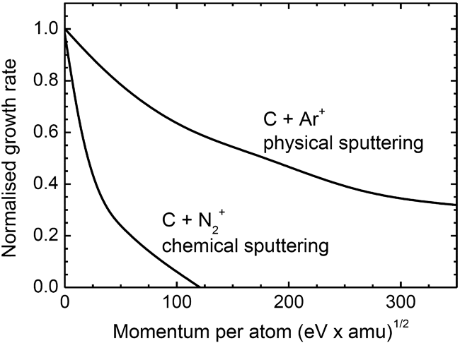
A very important point here is chemical sputtering, i.e., the formation and desorption of CxNy moieties.Reference Hammer and Gissler172 This effect was predicted by simulationsReference Todorov, Marton, Boyd, Albayati and Rabalais131 and studied in detail experimentally.Reference Hammer and Alvarez173 Some authors claim that chemical sputtering is responsible for the microstructure and properties of the films due to the formation of FL moieties acting as seeds.Reference Hellgren, Johansson, Broitman, Sandstrom, Hultman and Sundgren174Figure 13 shows how the film growth rate for carbon evaporation changes with Ar and N2 ion assistance, the former inducing only physical sputtering and the latter adding chemical sputtering effects.
Growth rate in IBAD assisted with Ar and N2 ions, normalized to the carbon evaporation rate, as a function of the momentum per impinging carbon atom. Adapted from Ref. Reference Gago, Jimenez, Agullo-Rueda, Albella, Czigany and Hultman175.
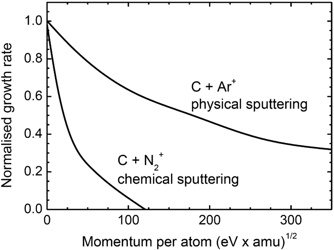
With regards to the synthesis by IBAD using carbon evaporation assisted with mixtures of N2+ and Ar+ ions, the optimal ion energy range to obtain a dense film, with the minimum ion induced damage, is about 100 eV, with a transport ratio close to unity. The reactivity between carbon and nitrogen to yield a solid compound is low, with a high tendency to form volatile moieties that are desorbed from the surface. As a result, the film-growth rate decreases significantly with N2+ assistance, as compared to bombardment with Ar+ ions of the same energy and transport ratio, as shown in Fig. 13. However, the incorporation of nitrogen into the film is only found for conditions that also induce chemical sputtering, as shown in Fig. 14. Both processes, nitrogen incorporation and chemical sputtering, are energy dependent.Reference Gago, Jimenez, Caceres, Agullo-Rueda, Sajavaara, Albella, Climent-Font, Vergara, Raisanen and Rauhala168
Growth rate and N incorporation in CNx films grown by carbon evaporation with nitrogen assistance, as a function of the ion energy. Adapted from Ref. Reference Gago, Jimenez, Caceres, Agullo-Rueda, Sajavaara, Albella, Climent-Font, Vergara, Raisanen and Rauhala168.

Nitrogen is incorporated in the film mainly in pyridine, cyanide, and substitutional graphite-like environments. The ratio of nitrogen atoms in these environments determines the structure and properties of the film, being the desired one the threefold graphitic that yields continuity to the graphene sheets. Substrate temperatures of ∼500 °C are required for the optimal FL structure. Regarding the microstructure, the material ranges between amorphous and nanocrystalline, without x-ray diffraction-long-range order, although TEM pictures show a certain orientation of basal planes or a FL structure (see Fig. 12).Reference Neidhardt, Czigany, Brunell and Hultman170 Neither crystalline grains nor crystallographic defects can be recognized although vacancies in the graphene sheets must be common according to the structural models proposed. The films are dense without any columnar growth or voids. However, textured films are common, despite the lack of long-range order, due to the compressive stress that tends to orient the basal planes perpendicular to the surface.
V. TERNARY BCN COMPOUNDS
The structural similarity between the allotropic forms of carbon and BN, and the fact that B–N pairs are isoelectronic to C–C pairs, has stimulated intensive research in the last decade toward the synthesis of ternary BCN compounds that may combine the advantages of C and BN.Reference Solozhenko, Andrault, Fiquet, Mezouar and Rubie176 Theoretical work has predicted the stability of such compounds both in cubicReference Tateyama, Ogitsu, Kusakabe, Tsuneyuki and Itoh177, Reference Sun, Jhi, Roundy, Cohen and Louie178 and hexagonalReference Liu, Wentzcovitch and Cohen179 forms. Cubic BCN compounds (c-BCN) are expected to combine the properties of diamond and c-BN, namely, extremely high hardness, chemical stability at high temperatures, and electronic gap of ∼6 eV, whereas hexagonal structures (h-BCN) are expected to behave as semiconductors with various band gap energies, ranging from metallic character for carbon-rich to wide gap semiconductors for carbon-depleted compounds. The first searched compound was BC2N because it is composed of an equal number of B–N pairs and C–C pairs and is a semiconductor with a gap around 2 eV.Reference Watanabe, Itoh, Mizushima and Sasaki180 Moreover, hexagonal phases can exhibit the FL structure observed in CNx.Reference Hellgren, Berlind, Gueorguiev, Johansson, Stafstrom and Hultman181
The first synthesis methods were based on CVD,Reference Kaner, Kouvetakis, Warble, Sattler and Bartlett182 but in this case, it was common to have a significant H content,Reference Weber, Bringmann, Nikulski and Klages183–Reference Polo, Martinez, Esteve and Andujar185 which is detrimental for the mechanical and electronic properties. H-free BCN coatings can be obtained by IBAD by a supply of B and C atoms concurrent to N2+ bombardment. The first reports were based on B4C evaporation from a single source, combined with ion bombardment,Reference Gago, Jimenez and Albella186–Reference Gago, Jimenez, Garcia and Albella188 being the transport ratio of ion to atom the controlling parameter of the transition from a boron carbide to a hexagonal BC0.25N.Reference Gago, Jimenez, Agullo-Rueda, Albella, Czigany and Hultman175 The same approach has been done by biased magnetron sputtering.Reference Johansson, Ivanov, Hultman, Munger and Schutze189 However, using B4C as the precursor for C and B has an intrinsic limitation in the ratio B/C = 4, which excludes formation of C-rich solids. In the case of hexagonal compounds, the carbon limit of 11 at.% corresponding to the composition BC0.25N has been observed experimentally. Such a ternary phase was identified by new spectroscopic features indicative of carbon incorporation in the hexagonal BN structure.Reference Gago, Jimenez, Albella and Terminello190 However, when the IBAD growth conditions are those for the synthesis of c-BN, namely high substrate temperature (∼500 °C) and bombardment with a mixture of Ar and N2 ions at 500 eV, but using B4C evaporation instead of B, one obtains a c-BCN with a C content of about 5 at.%, hence lower than that of h-BC0.25N, due to preferential sputtering of carbon when Ar bombardment is incorporated, or its limited solubility in the c-BN matrix.Reference Gago, Jimenez, Sajavaara, Rauhala and Albella191
To overcome the carbon concentration limit using evaporation from a single B4C source, one possibility is to add a hydrocarbon gas, like methane or acetylene, to the feed of the ion gun. In this case, a mixture of nitrogen and CxHy+ ions is used as assistance, and BCN films richer in carbon are obtained, but at the expense of a small H incorporation.Reference Gago, Jimenez, Kreissig and Albella192 The same approach has been tried by sputtering in a mixture of gases containing hydrocarbons.Reference Ulrich, Ehrhardt, Theel, Schwan, Westermeyr, Scheib, Becker, Oechsner, Dollinger and Bergmaier193
However, to get full control on the synthesis of ternary BCN films, the best strategy is to use independent B, C, and N sources. In the case of IBAD, this is accomplished by using two independent evaporation sources for boron and carbon, plus the ion gun for nitrogen ion assistance, as was described in Fig. 2.Reference Caretti, Jimenez and Albella194 In the case of biased magnetron sputtering there are three possibilities (i) cosputtering from independent B (or B4C) and C targets under N2/Ar atmospheres,Reference Knotek, Lugscheider and Siry195 (ii) RF cosputtering from independent h-BN and C targets,Reference Zhou, Bello, Lei, Li, Lee and Lee196 and (iii) using special targets with different B/C ratios.Reference Ulrich, Kratzsch, Leiste, Stuber, Schlossmacher, Holleck, Binder, Schild, Westermeyer, Becker and Oechsner197–Reference Linss, Barzola-Quiquia, Haussler and Richter200
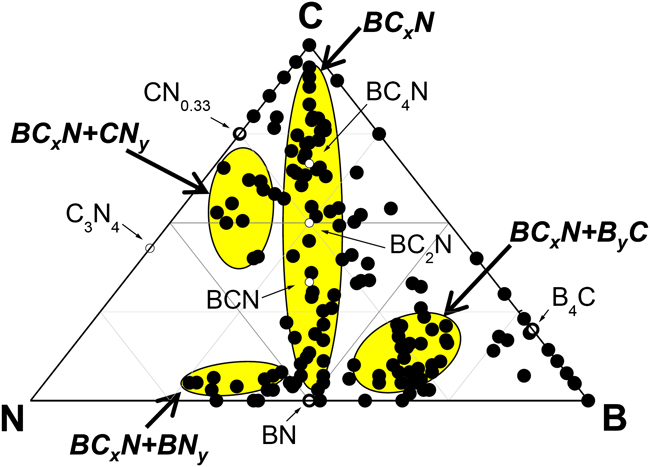
According to the above isostructural and isoelectronic premises, a stable ternary BCN compound should have a BCxN composition, i.e., equal number of boron and nitrogen atoms, to fulfill charge neutrality conditions. Otherwise, the ternary compound is not stable and may decompose into segregated phases (C, BN, B4C, CNx, etc). This situation is sketched in the BCN ternary diagram of Fig. 15, which displays as black dots the experimental composition values from a large set of samples grown by IBAD using a broad range of B/C/N independent fluxes. Reference compounds are marked with white dots and labeled, and several composition regions are marked with shadowed areas and labeled in bold. One can identify that many of the experimental points gather in a region around the vertical BCxN line, as marked in the figure, and several subsets as N-rich borides, B-rich carbides, and mixed phases of BCxN with an excess of BxC, BNx, and CNx. Also, it can be recognized that BCN compounds with a N content above ∼60% are not present.
Ternary BCN diagrams with actual compositions obtained by IBAD (black dots). Reference compounds are marked with white dots and several composition regions with colored areas.

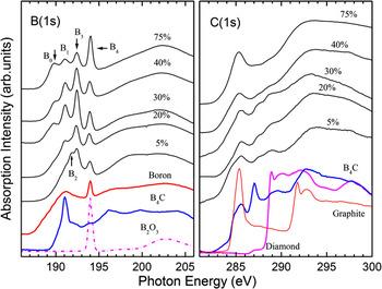
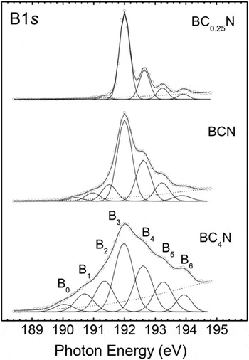
Studies of the bonding structure of carbon-rich h-BCxN films by XANES has found evidence of the mixing of the B, C, and N atoms in the same planes by coordination of a boron atom to different number of C and N neighbors, i.e., B–N3, B–CN2, B–C2N, and B–C3Reference Caretti and Jimenez110 environments, as is depicted in Fig. 16.
B(1s) XANES spectra for ternary BCxN films with different carbon contents, evidencing the formation of bonding environments of B atoms to different number of C and N neighbors. From Ref. Reference Caretti and Jimenez110.

Although the synthesis of ternary BCN compounds is possible, only in a few reports the production of a real ternary compound is clear, since the presence of B–C, B–N, and C–N bonds is not enough to discern between a true ternary phase and a mixture of segregated binary phases. In fact, this is still a controversial point and it seems that one needs to finely adjust the B/C/N fluxes to obtain a ternary with a BCxN composition, otherwise there is phase segregation. In this sense, some authors have reported phase segregation in BCN coatings prepared by sputtering,Reference Ulrich, Ehrhardt, Theel, Schwan, Westermeyr, Scheib, Becker, Oechsner, Dollinger and Bergmaier193, Reference Morant, Prieto, Bareno, Sanz and Elizalde201 but more recent work by IBAD using independent B/C/N fluxes finds a homogeneous ternary compound without segregation at a nanometric level, even for a carbon-rich material with the composition BC4N.Reference Chen, Yu, Zhao, Ren, Ding, Shi and Liu78, Reference Caretti, Torres, Gago, Landa-Canovas and Jimenez202 This result is shown in Fig. 17, where element-filtered TEM images show a homogeneous distribution of BCN atoms in an amorphous BC4N film. The growth conditions, with the substrate at room temperature and using only nitrogen bombardment, were typical for hexagonal BCN growth and the amorphization is explained by the carbon incorporation in the basal planes. The problematic of discerning between a ternary phase and a mixture of binary nanodomains is an open question that also concerns well-ordered nanomaterials. In the case of h-BCN, some authors claim the formation of separated sheets of BN and C with sequential stacking, whereas others have found coexistence of C and BN nanodomains in the same plane.Reference Ci, Song, Jin, Jariwala, Wu, Li, Srivastava, Wang, Storr, Balicas, Liu and Ajayan203
Energy-filtered TEM images of the a-BC4N compound showing a homogeneous distribution of boron, carbon, and nitrogen elements all along the amorphous material. From Ref. Reference Caretti, Torres, Gago, Landa-Canovas and Jimenez202.

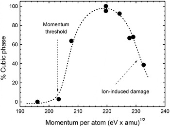
Despite the relative ease to obtain hexagonal or sp2-bonded BCN with controlled composition using independent sources of B, C, and N, the synthesis of cubic or sp3-bonded BCN with large carbon contents has not been successful up-to-date, remaining an open research field. The sp3 phase has only been observed for BCN compounds with a low carbon content (below 5 at.%) and is obtained for growth conditions similar to those of c-BN growth, in particular a substrate temperature near 500 °C, a mixture of Ar and nitrogen ions near 50%, and ion energies around 500 eV.Reference Gago, Jimenez, Sajavaara, Rauhala and Albella191 The dependence of the fraction of sp3-bonded BCxN with the growth parameters can be represented as a function of a single variable, the momentum per deposited atom, as is done in Fig. 18. This parameter contains information on the energy and mass of the ions and the transport ratio, (see Sec. III.A). A similar dependence of sp3 phase promotion with momentum transfer has been reported for BCxN films grown by magnetron sputtering,Reference Ulrich, Kratzsch, Leiste, Stuber, Schlossmacher, Holleck, Binder, Schild, Westermeyer, Becker and Oechsner197 but were interpreted as segregated c-BN and C nanograins. However, the local bonding structure of the B, C, and N atoms observed by XANES in Ref. Reference Gago, Jimenez, Sajavaara, Rauhala and Albella191 indicated the formation of ternary phases.
Dependence of the sp3 fraction in BCxN obtained by IBAD of B4C assisted with Ar and nitrogen ions, as a function of the single-parameter momentum tranfer per deposited atom.

The hitherto obtained BCN coatings have shown interesting mechanical and tribological characteristics, comparable or superior in some cases to carbon and CNx coatings.Reference Zhou, Adachi and Kato204, Reference Zhou, Adachi and Kato205 Tribological measurements indicate that C-rich BCxN are the most interesting coatings,Reference Chen, Wang, Ma, Ji and Chu206, Reference Caretti, Jimenez, Gago, Caceres, Abendroth and Albella207 in particular those with the composition BC4N,Reference Caretti, Albella and Jimenez208, Reference Caretti, Albella and Jimenez209 and this is explained by an structural change from hexagonal to amorphous structureReference Caretti, Torres, Gago, Landa-Canovas and Jimenez202 upon carbon intake. The tribological performance of several BCxN coatings has been tested under different atmospheres and also with different lubricant liquids.Reference Chen, Zeng, Yang and Zhang210
Regarding electronic applications, their practical use as a semiconductor is still unclear. However, BCN has proved to be an excellent low-K dielectric material.Reference Aoki, Watanabe, Moriyama, Mazumder, Komatsu, Kimura and Sugino211 Other electrical applications are as negative electrodes in battery systems.Reference Ishikawa, Nakamura, Morita, Matsuda, Tsujioka and Kawashima212
More complex materials under investigation are quaternary compounds which add a fourth element to BCN, like BCNO,Reference Ong, Chan, Zhao and Choy213 SiBCN,Reference Vlcek, Potocky, Cizek, Houska, Kormunda, Zeman, Perina, Zemek, Setsuhara and Konuma214 TiBCN,Reference Vyas, Lu and Shen215 WBCN,Reference Kim and Lee216 and other metal–BCN systems. A particularly interesting system is SiBCN because the intrinsic sp3 hybridization of Si atoms is believed to force the tetrahedral coordination of the accompanying B, C, and N atoms.
Regarding research in BCN nanomaterials, at present there is also a renewed interest not only for BCN nanotubesReference Yu, Ahn, Yoon, Zhang, Rusli, Gan, Chew, Yu, Bai and Wang217 and nanoparticlesReference Torres, Caretti, Gago, Martin and Jimenez218 but also for ultrathin BCN analogues of graphene.Reference Raidongia, Nag, Hembram, Waghmare, Datta and Rao15, Reference Ci, Song, Jin, Jariwala, Wu, Li, Srivastava, Wang, Storr, Balicas, Liu and Ajayan203, Reference Venu, Kanuri, Raidongia, Hembram, Waghmare and Datta219
VI. MULTILAYERS
In this section, we summarize the developments dealing with the stacking of some of the materials discussed in the preceding sections to form multilayer systems. We are excluding in the discussion most of the multilayers formed with other materials, mainly transition metal nitrides (Ti, Al, Cr, Zr,..), for which there is an abundant literature.
A. Boron- and B4C-containing multilayers
The formation of boron multilayers was aimed toward the fabrication of periodic structures for x-ray mirrors, alternating high-Z (typically W) and low-Z (typically B and B4C) materials.Reference Jankowski, Schrawyer and Wall220 There is also work dealing with the structure and mechanical performance of nanometric period multilayers alternating the hard material B with the soft h-BN.Reference Jankowski and Hayes221 More recent work combines two hard borides to form multilayers like TiB2/B4C.Reference Andrievski222
B. BN-based multilayers
The quest for stress-free c-BN films has explored the use of alternating layers of cubic and hexagonal boron nitride. The idea is to release in the h-BN layers the compressive stresses related to the c-BN layers.Reference Guruz, Dravid and Chung223 The crack propagation in such structures has also been studied.Reference Kurooka, Ikeda and Iwamoto224
C. CNx/BN multilayers
Periodic multilayers of carbon nitride and boron nitride have been grown aiming toward increasing the wear resistance by prevention of fracture growth at the interface of each layer.Reference Miyake225, Reference Miyake226 These multilayers have been grown with FL CNx, showing an improved system response (stiffer and more elastic) compared to monolithic FL CNx.Reference Johansson, Hellgren, Berlind, Broitman, Hultman and Sundgren227
D. BCN-based multilayers
There are scarce results about multilayers of ternary BCN compounds, discussing basic aspects of growth and structural matching at interfaces. The reports are based on exploratory work of properties improvement, like corrosion resistance,Reference Moreno, Caicedo, Amaya, Cabrera, Yate, Aperador and Prieto228 stabilization of c-BN phases by a sequential stacking of B4C/BCN/c-BN,Reference Bejarano, Caicedo, Baca, Prieto, Balogh and Enders229 formation of a BCN/CN/BN multilayer,Reference Morant, Caceres, Sanz and Elizalde230 or the interesting concept of making a gradient layer grown with different bias voltages (ion energies) to reduce the film internal stress.Reference Kratzsch, Ulrich, Leiste, Stuber and Holleck231 There are some work on the combination of BCN layers with transition metal nitrides, like TiNReference Fayeulle and Nastasi232 or CrN,Reference Yamamoto, Kujime and Takahara233 the latter reporting an excellent tribological performance.Reference Yamamoto, Ito and Kujime234
ACKNOWLEDGMENTS
We acknowledge financial support from the Ministry of Science and Innovation projects Consolider FUNCOAT CSD2008-0023, MOCASIN MAT2010-21070-C02-02, and FIS2009-12964-C05-04. R. Torres and I. Caretti acknowledge support from CSIC through JAE and JAE-Doc fellowships.