I. INTRODUCTION
Direct momentum transfer from charged particles to atoms of the sample is one of the main physical mechanisms for ion-beam damage and for expelling atoms from their lattice positions.Reference Livengood1 If one wants to remove material from the surface of a sample—for instance to create a hole—one can use a range of charged particles such as ions or electrons. Ions are preferable due to their mass. However, implantation of the ions into the sample may cause significant lattice damage in the illuminated area as well as its surroundings and can result in surface degradation of the remaining structure.Reference Raineri and Saggio2 To analyze the influence of the ion beam on the illuminated sample, three forms of damage should be considered: surface sputtering of atoms, displacement of atoms in the sample from their original lattice positions and implantation of the incident ions into the sample.Reference Livengood1 Calculations based on computer program “Transport of Ions in Matter” (TRIM) show that in the case of relatively heavier ions such as that of gallium (Ga), 90% of energy is dissipated through the ion's interaction with nuclei. For 25 keV He ions, 6.7% of this energy is dissipated through the ion's interaction with nuclei whereas 93.3% of the energy is transferred to electrons. Lighter ions, such as that of helium (He), have a lower energy loss rate, and therefore they penetrate much deeper into the specimen than the heavier Ga ions. The average energy loss rate for 25 keV He ions in silicon is 89 eV/nm.Reference Ziegler, Biersack and Ziegler3 Implantation of He ions deep into the sample can be discounted, as hardly any He ion is implanted in the first few nanometers, whereas serious subsurface damage is caused by heavier ions. This makes the He ion a suitable candidate for precise nanoscale modification of the samples or ion beam-induced surface chemistry.Reference Maas, van der Drift, van Veldhoven, Meessen, Rudneva, Alkemade, Baglin, Ila, Marletta and Ӧztarhan4, Reference Alkemade, Koster, van Veldhoven and Maas5
The helium ion microscope (HIM) was introduced in 2006 as a new high-resolution imaging tool.Reference Ward, Notte and Economou6 The unique He-ion source can be regarded as the nearly ideal point source, because it results in a subnanometer probe size, which generates a large depth of view. When compared with other ions, He ions have a particular sample interaction that generates a relatively high number of low-energy secondary electrons and a low yield of backscatter ions, which allows the remarkable imaging of a range of samples, including samples with high local specimen charging.Reference Maas, van der Drift, van Veldhoven, Meessen, Rudneva, Alkemade, Baglin, Ila, Marletta and Ӧztarhan4, Reference Bell7, Reference Postek, Vladar, Archie and Ming8
Being used for nanofabrication, HIM is reported to yield 4-nm-wide lines with a pitch of 10 nm as lithography tool.Reference Sidorkin, van Veldhoven, van der Drift, Alkemade, Salemnik and Maas9, Reference Winston, Cord, Ming, Bell, DiNatale, Stern, Vladar, Postek, Mondol, Yang and Berggren10 Very narrow structures with almost no overspray can be made with the gas-induced deposition.Reference Maas, van Veldhoven, Chen, Sidorkin, Salemink, van der Drift and Alkemade11, Reference Drezner, Greenzweig, Fishman, van Veldhoven, Maas, Raveh and Livengood12 For thin-film dicing and nanopore drilling, sub-10-nm features are now achieved.Reference Lemme, Bell, Williams, Stern, Baugher, Jarillo-Herrero and Marcus13, Reference Yang, Ferranti, Stern, Sanford, Huang, Ren, Qin and Hall14
It is known that penetration of the accelerated He ions into bulk samples, e.g., in Si, leads to amorphization, the formation of nanobubbles and even microbubbles at high doses.Reference Livengood1 In this article, we demonstrate the possibility of performing defect-free cutting of silicon (Si) and strontium titanate (SrTiO3) lamellae of various thicknesses at elevated temperatures. Also results of precise modification of thin Pt bridges with a He beam are presented.
II. EXPERIMENTAL
Silicon and SrTiO3 lamellae of 6 × 10 μm2 with different thicknesses were prepared by gallium focused ion-beam (Ga-FIB) milling. In that case, the milling is the result of an interaction of heavy Ga ions with matter. This expels atoms from the surface, but at the same time may appear as a subsurface damage and as Ga contamination of the sample. For removing these undesired effects, a last nanoscale modification step should be performed with, for example, a HIM.
A helium ion microscope (HIM; ORION PLUS, Carl Zeiss SMT, equipped with a Raith ELPHY MultiBeam pattern generator) is used. The microscope is normally operated at 25 kV. The beam currents for the cutting are set between the 1.5 and 4 pA and are easily controlled with the He gas supply. The pattern generator controls the number of scans, illuminating area and beam path and enables cuts of almost any form. To follow the cutting process, images are recorded by an Everhart-Thornley (ET) detector. Imaging of the sample prior and after cutting does not affect the sample. We have estimated the rate of 1015 ions/cm2 based on number of scans, beam current and the size of the illuminated area. It is not unreasonable to speculate that this number underestimates the actual rate. One way of improving the measurement of the rate in our experiment is the use of a Faraday cup, this is planned in the future.
For in situ HIM modification at elevated temperatures microelectromechanical systems (MEMS)-based heatersReference van Huis, Young, Pandraud, Creemer, Vanmaekelbergh, Kirkland and Zandbergen15 were used as a substrate for the lamellae. Each heater has a few through holes in the membrane and FIB-prepared samples were placed over those holes using a micromanipulator.
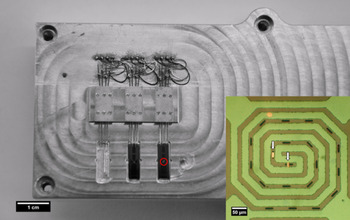
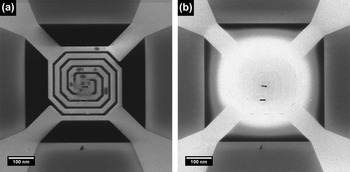
A special holder was developed to load up to three MEMS-based heaters with specimens to be examined (Fig. 1). Special needle-like clamps allow each heater to be fixed to the holder and at the same time provide a good electrical contact between heaters and the electronics of the holder. Each MEMS heater can be turned on or off without being removed from the microscope. To switch the heater a special detector is embedded into the box. The switching occurs by illuminating the detector with the He-ion beam with beam current of ∼200–300 pA, whereby the number of pulses detected defines which heater will be activated or switched off. It is possible to judge by direct observation whether the heater is on or off (see Fig. 2). The temperature of each heater is set using a calibrated resistor. Application of the heating stage allows heating the sample from room temperature to 800 °C.
Optical image of the heating stage with two heaters; Inset is a blowup of the red encircled region showing heater with two Si lamellae located above the holes in the SiN membrane.

Two states of the heater: (a) heater is off; (b) heater is on.

We analyzed the HIM-modified samples with a transmission electron microscope (TEM; TITAN3, FEI Company, operated at 300 kV) to determine sample modification related to He-ion implantation.
III. RESULTS
A. Modification of Si lamellae at different temperatures
Silicon is one of the most commonly used materials in the semiconductor industry. Ongoing development and miniaturization of semiconducting devices requires new techniques for sample modification and reparation in case of any possible failure or damage. Focused ion beam (FIB) microscopy using Ga ions has demonstrated good results for bulk samples so far. However, the lack of resolution, significant broadening of the beam near the surface and contamination of the sample with Ga ions make Ga-FIB nanomodification of the samples nearly impossible.Reference Rue, Shepherd, Hallstein and Livengood16 In that sense it is necessary to develop new cutting techniques that allow the sample to be modified on the scale of a few nanometers without causing significant damage or contamination.
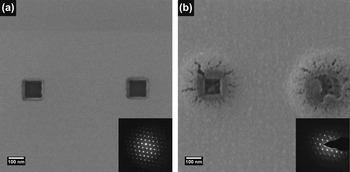
A few holes of 100 × 100 nm2 were created in Si lamellae at room temperature to check the effect of the sample thickness. Figure 3 shows HIM images and electron diffraction patterns from the illuminated area for samples with a thickness of 100 nm [Fig. 3(a)] and 300 nm [Fig. 3(b)]. For 100-nm-thick Si samples, no damage is observed around the cut on HIM image, whereas for the 300-nm-thick Si samples, big deformation structures were created in the area of modification (see Fig. 4). It is evident from extra spots and diffuse background in the diffraction patterns obtained with TEM that, in the case of room temperature milling, lattice deformation is observed for 300-nm-thick samples. This shows that defect-free cutting of thick Si samples is not possible at room temperature for thicker samples.
Result of cutting Si lamellae with a thickness of (a) 100 nm and (b) 300 nm at room temperature. Boxes measuring 100 × 100 nm2 were scanned with a helium beam at the same dose. Diffraction patterns in the insets indicate that the crystallinity of the area around the cut was substantially affected in the case of the 300-nm-thick sample.

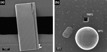
(a) Si lamella placed above the hole in MEMS heater at room temperature; (b) results of cutting of Si lamella at room temperature and at 700 °C. As can be seen, at room temperature a large bright halo appeared around the illuminated area, whereas at 700 °C it was possible to create a through hole in the lamella.

To prevent bubble formation, out-diffusion of He from the sample should be enhanced.Reference da Silva, Morschbacher, Fichtner, Oliviero and Behar17, Reference David, Beaufort and Barbot18 This can be done by keeping the sample at a higher temperature during a cutting process.
To determine the influence of the temperature on the process of modifying the samples with a focused He-ion beam, Si lamellae of different thicknesses were placed on the MEMS heaters. Temperature of the heaters was set to 700 °C. Figure 4 shows the result of cutting a 100 × 100 nm2 box out of 300-nm-thick Si lamella at room temperature and at 700 °C, respectively. In the case of the room temperature cutting, a large bright halo appeared around the cut area. The diameter of the damaged area is ∼300 nm, which is in good agreement with the expected He-ion distribution in Si (see Sec. IV). TEM inspection and diffraction patterns taken from this area indicate that deformation and even amorphization of the surrounding area occurs. At 700 °C it is possible to obtain a clean cut without any visible damage [Fig. 4(b), top box].
B. Nanoscale modification of SrTiO3
Oxides with a perovskite structure have a large variety of properties and, because of similarities in unit cells, they are often being stacked or used as thin films on other oxide substrates with a perovskite structure.Reference Jia, Thust and Urban19 One of the frequently used perovskite substrates is SrTiO3. This is a dielectric with a simple cubic unit cell; however, a deviation in stoichiometry and in geometry may induce additional electrical properties such as conductivityReference Szot, Speier, Carius, Zastrow and Beyer20 and ferroelectricity.Reference Haeni, Irvin, Chang, Uecker, Reiche, Li, Choudhury, Tian, Hawley, Craigo, Tagantsev, Pan, Streiffer, Chen, Kirchoefer, Levy and Schlom21 In the TEM characterization of thin films on SrTiO3 substrates, we are particularly interested in the film—SrTiO3 interface to determine intermixing and interface roughness. Conventional TEM sample preparation techniques, such as cross section low-angle broad beam ion milling and focused Ga ion-beam milling, can provide such information. However if one would like to thin down a specific area to obtain more detailed information, additional thinning with the conventional techniques is almost never successful.
With the HIM, it might be possible to remove material over the defect or to create a wedge-shaped sample. The well-defined wedge shape allows the very precise investigation of the changes in high-resolution TEM images as a function of thickness. This can provide details of atom positions with various scattering potentials such as O next to Sr and Ti. Although the HIM allows the selected removal with high precision, the quality of this cut still remains an open question.
A few SrTiO3 lamellae of various thicknesses were prepared by FIB milling. Further thinning down of the sample as well as creation of the holes and wedge-shaped cuts were accomplished by focused He-ion beam. Experiments were performed for different ion doses, controlled by beam current and number of scans.
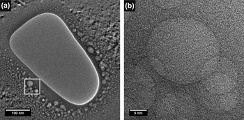
Cutting experiments on a 100-nm-thick sample show the formation of nanobubbles around the hole (Fig. 5) at room temperature. Moreover significant degradation and amorphization of the area close to the cut is observed by TEM inspection of the sample. For a thicker sample, bigger bubbles are present around the formed hole and the crystallinity is completely lost in the area [Fig. 6(a), top].
Result of cutting a SrTiO3 lamella at room temperature. (a) Overview of the illuminated area. (b) Nanobubbles formed around the hole.

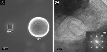
Result of modification of a SrTiO3 lamella at (a) room temperature (top) and 650 °C (down). At room temperature, numerous bubble-like defects were formed near the modified area. At 650 °C, no visible defects were created around the cut at these conditions; (b) TEM image of the hole made in a SrTiO3 sample at 650 °C. Lattice planes are clearly visible, confirming that the sample remains crystalline up to the edge. The arrow on the top corner shows the crystalline edge after He cutting.

The HIM heating stage was used for carrying out the experiments at elevated temperatures. For this purpose we used a few 150 nm SrTiO3 lamellae on MEMS heaters. The heaters temperature was set to 650 °C. As can be seen from Fig. 6(a), the hole made at 650 °C has a completely different appearance than the hole made at room temperature. It is obvious that at room temperature, the area around the cut is strongly affected [Fig. 6(a), top], whereas at 650 °C, it is possible to obtain a clean cut without any visible damage. The sample was checked using TEM [Fig. 6(b)]. Inspection shows the absence of bubbles or an amorphous phase and that the crystalline structure of SrTiO3 is present up to the edge of the cut [see Fig. 6(b)].
C. Nanoscale modification of Pt bridges for transmission electron microscopy study
To fabricate metallic lines serving as contacts to nanowires or carbon (C) nanotubes, one commonly uses optical and e-beam lithography. These fabrication methods are quite time-consuming and costly, and therefore such structures/devices are produced in batches. If one is interested in local modification/changing of batch-produced samples, it is necessary to perform the entire lithography process again. Thus it would be useful to have a tool for making quick local modifications to the sample. The main requirement of such a tool is that it induces no significant damage to the surrounding areas. On a scale >40 nm, a focused Ga ion beam can be used, but it is known that it leads to a significant modification of the surface layer and introduces Ga contamination to the sample. The He-ion microscope can be considered a better tool because it uses lighter He ions instead of heavier Ga ions and because virtually no chemical interaction of the He ions with atoms of the target will occur.
For checking the applicability of the HIM for local modification of the TEM samples made by lithography, we selectively cut thin polycrystalline Pt bridges deposited onto membrane to create various shapes. Obviously the reason to make these shapes is to correlate changes in geometry for those samples with changes in their properties; e.g., electrical measurements can be performed.Reference Rudneva, Gao, Prins, Xu, van der Zant and Zandbergen22
Polycrystalline platinum bridges and gold electrical contacts were produced on the silicon nitride (SiXNY) membrane in two steps, namely e-beam lithography and subsequent CVD deposition. The bridges have dimensions of 200 × 300 × 15 nm3 and the thickness of the membrane is 100 nm. Details of the sample fabrication process can be found in Ref. Reference Gao, Rudneva, McGarrity, Xu, Prins, Thijssen, Zandbergen and van der Zant23. These structures have been used as test samples to demonstrate the capability of a HIM to yield the desired shape.
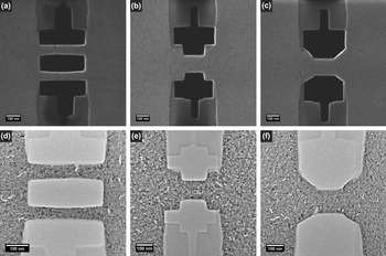
It is possible to modify the samples to the desired shape by manual control or by use of a special pattern-generating program. In the presented experiments Raith ELPHY MultiBeam pattern generator was applied for modification of the bridges. Pictures of the modified bridges obtained with a HIM and a TEM are shown in Fig. 7. From a large variety of HIM-made shapes, we selected the most illustrative ones: (i) two thin, freestanding bridges with a width of ∼50 nm are separated by a 100-nm pitch; (ii) a resized bridge measuring W = W 0/2 and L = L 0/2 as compared with the original bridge and with edges perpendicular to the contacts; (iii) a resized bridge measuring W = W 0/2 and L = L 0/2 compared with the original bridge and with edges that are at a 45° angle to the contacts. Also in all cases, the SiXNY membrane around the bridges was removed without affecting the bridges.
(a, b, c) HIM and (d, e, f) corresponding TEM images of Pt bridges modified by a HIM.

A TITAN3, FEI Company, was used to study the samples and to analyze both the purity of the cuts and the damage caused by a He beam. High-resolution TEM inspection reveals that the Pt lattice is visible up to the cutting edge and that artifact-free cutting of Pt can be done with the HIM.
IV. DISCUSSION
Ongoing developments in TEM require new possibilities for sample investigation and at the same time require new and more accurate sample preparation techniques. The HIM could be a great tool for the preparation of samples for TEM, if it has a sufficient throughput and creates no or very limited damage to the fabricated electron transparent specimens. The He-ion impact on all kinds of materials is not yet known. Thus its usefulness for the TEM sample preparation, in particular for composites, still has to be determined.
The experimental results presented in this article show that the HIM can be used as an artifact-free cutting tool. Although for some samples like layered CuxBi2Se3 or Pt nanowires modification can be done already at room temperature,Reference Rudneva, van Veldhoven, Maas and Zandbergen24 most of the samples require heating to provide fast out-diffusion of the implanted He atoms before they form irreversible defects. In addition to the out-diffusion of He, the deposition depth profile also plays an important role, providing that for thin enough samples even room temperature sculpting can be done. Our experiments show that for drilling a hole in 100-nm thick Si at room temperature, the damage, created on the remaining area in close proximity to the hole, is so small that no effect of implanted He is visible in the HIM image or the electron diffraction patterns whereas abundant defects are present in the 300-nm thick sample.
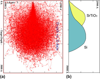
TRIM simulations of the stopping range of He ions at 25 kV in Si (Fig. 8) represent that the distribution of the deposited He ions has a Gaussian shape with maximum (mean projected range) at ∼250 nm. For a sample thickness of ∼100 nm, only a small fraction of the He ions is stopped in the sample and furthermore the interaction volume is small due to the high collimation of the beam. Therefore the interaction of He with Si samples thinner than about 100 nm should not create serious damage even at room temperature, as indeed observed experimentally and shown in Fig. 3(a). However, if one wants to modify thicker Si samples using a He beam, significant damage to the sample is expected. In the case of SrTiO3, the penetration depth is less (the mean projected range is 130 nm for 25 kV He ions) and sample damage is expected to occur at room temperature even for thin samples.
(a) TRIM simulation of 25 kV He-ion trajectories in Si; (b) comparison of He-ion distribution in SrTiO3 and Si. Statistical depth distribution is based on the simulation of 4000 ions.

The TRIM calculations are in good agreement with our experimental data and with previous studiesReference Livengood1, Reference Postek, Vladar, Archie and Ming8 showing that at high enough dose, Si within ion propagation path becomes completely amorphous and small nanobubbles are formed in the amorphous region. Further implantation of He ions leads to a deformation of the amorphous surface layer and the formation of a balloon-like structure.Reference Reutov and Sokhatskii25
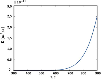
The diffusion is exponentially dependent on temperature.Reference Jung26 This dependence for Si sample is plotted in Fig. 9. As can be seen from the plot heating of the sample will strongly accelerate the out-diffusion if temperature is high enough. For both Si and SrTiO3 the out-diffusion at around 650 °C is large enough to prevent the formation of defects.
Temperature dependence of out-diffusion of He from Si sample.

V. CONCLUSIONS
We have investigated the effect of specimen temperature on the damage created by a focused He beam in Si and SrTiO3 samples. It is clearly essential to heat the sample to prevent damage due to the embedded He ions. If the out-diffusion of He is sufficiently large, high-quality cuts can be made.
We have shown that heating the sample makes HIM an excellent tool for nanoscale modifications for simple systems like Si and SrTiO3. However more complex samples (e.g., parts of ICs) may suffer from unwanted diffusion of such things as dopants, barrier layers or Cu metallization, all of which put an upper limit on the allowed temperature. Further studies of the process conditions (scan strategy, beam current variations etc.) are needed to determine the best processing window for such complex samples.