I. INTRODUCTION
So-called “nanostructured” materials,Reference Gleiter1 which have characteristic feature sizes of the order of a few to tens of nm, are attractive in a wide range of applications including energy storage,Reference Arico, Bruce, Scrosati, Tarascon and Van Schalkwijk2–Reference Bruce, Scrosati and Tarascon5 thermoelectrics,Reference Dresselhaus, Chen, Tang, Yang, Lee, Wang, Ren, Fleurial and Gogna6 photovoltaics,Reference Gratzel7 chemical sensors,Reference Huang and Choi8–Reference Yu, Liang, Cho and Caruso10 photodetectors,Reference Konstantatos and Sargent11 drug delivery,Reference LaVan, McGuire and Langer12 and structural applicationsReference Wang, Chen, Zhou and Ma13 and can be produced via a variety of methods including chemical/physical vapor deposition,Reference Gleiter1 micromachining,Reference LaVan, McGuire and Langer12 and electrochemical cycling.Reference Choi, McDonough, Jeong, Yoo, Chan and Cui14 One of the more interesting methods of nanostructuring is via the use of ion beam modification (interchangeably referred to as ion-implantation). In particular, for the case of a few different types of semiconducting materials, ion beam modification under appropriate conditions is known to result in complete structural decomposition of a material with no or very little initial porosity to a porous microstructure consisting of a nanoscale interdigitated network of strands. This process is known to occur for several different semiconductors, and was first demonstrated for the case of compound semiconductors such as indium antimonide (InSb), gallium antimonide (GaSb), and gallium nitride (GaN).Reference Destefanis and Gailliard15–Reference Shaanan, Kalish and Richter19 However, It was not until the early 1980s that it was discovered that the elemental semiconductor Ge also experiences a similar phenomenon,Reference Appleton, Holland, Narayan, Schow, Williams, Short and Lawson20–Reference Lawson, Short, Williams, Appleton, Holland and Schow23 which has to date been most extensively studied as compared with any other materials that exhibit similar behavior. Nanostructuring of Ge using ion beam modification will be the subject of this review, but it should be noted that many, if not all, considerations discussed here in the context of Ge may not be applicable to the aforementioned materials that exhibit similar phenomena.
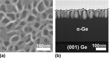
The basic process of structural decomposition of Ge using ion beam modification is described as follows: starting with a single-crystal Ge substrate, if the material is ion-beam modified with relatively heavy ions up to a critical dose, an amorphous (α) layer will form in the material, the extent of which depends mainly on the energy of the incident ions; if the dose is further increased beyond this amorphization threshold, the material will begin to structurally decompose and exhibit macroscopic voiding and porosity; with further increasing dose, the material eventually transforms into the aforementioned morphology consisting of a nanoscale interdigitated network of strands. Figure 1 presents top-down scanning electron microscopy (SEM) and cross-sectional transmission electron microscopy (XTEM) images showing an initially single-crystal Ge specimen that was rendered into the nanostructured morphology by Ge+-implantation at 260 keV at room temperature to a dose of 1.0 × 1016 cm−2. This morphology as been variously referred to by many different labels over several decades of study as “voided,” “porous,” “nanoporous,” “cratered,” and “honeycomb,” but for the purpose of this study, this morphology will be referred to as “nanostructured” as first termed by Romano et al.Reference Romano, Impellizzeri, Tomasello, Giannazzo, Spinella and Grimaldi24
Images of nanostructured Ge formed by Ge+-implantation at 260 keV at room temperature to a dose of 1.0 × 1016 cm−2 into single-crystal (001) Ge: (a) top-down SEM and (b) XTEM (surface indicated by dotted line).

As previously mentioned, the structural decomposition of Ge due to ion beam modification has been extensively studied and characterized by several independent research groups over several decades. The process is known to be most sensitive to ion dose,Reference Wilson21, Reference Romano, Impellizzeri, Tomasello, Giannazzo, Spinella and Grimaldi24–Reference Romano, Impellizzeri, Bosco, Ruffino, Miritello and Grimaldi28 specimen temperature during implantation,Reference Appleton, Holland, Narayan, Schow, Williams, Short and Lawson20, Reference Stritzker, Elliman and Zou27, Reference Glover, Ridgway, Byrne, Yu, Foran, Clerc, Hansen and Larsen29, Reference Ridgway, Glover, Yu, Foran, Clerc, Hansen and Larsen30 and, most interestingly, the nature of the starting material prior to ion beam modification (amorphous versus crystalline).Reference Romano, Impellizzeri, Bosco, Ruffino, Miritello and Grimaldi28, Reference Yates, Darby, Elliman and Jones31 However, while the structural decomposition of Ge has been studied and characterized empirically quite extensively, the fundamental understanding of nanostructuring due to ion beam modification remains a topic of debate. To date, two fundamentally different models have been advanced to explain the origin of structural decomposition due to ion beam modification: vacancy clustering and “microexplosions.” The vacancy-clustering modelReference Holland, Appleton and Narayan22, Reference Romano, Impellizzeri, Tomasello, Giannazzo, Spinella and Grimaldi24, Reference Ridgway, Glover, Yu, Foran, Clerc, Hansen and Larsen30, Reference Chen, Wilson, Cheung, Xu and Wong32–Reference Ottaviano, Verna, Grossi, Parisse, Piperno, Passacantando, Impellizzeri and Priolo34 is based on the premise of inefficient recombination of point defects in the material (which is known to be the case for GeReference Kogler, Mucklich, Skorupa, Peeva, Kuznetsov, Christensen and Svensson35) generated due to ion beam modification, which results in an excess quantity of vacancies that coalesce to form macroscopic voids. In contrast, the microexplosion modelReference Bellon, Chey, Vannostrand, Ghaly, Cahill and Averback36–Reference Mayr and Averback39 is based on the creation of voids through pressure waves and thermal spikes due to the overlap of ion cascades during ion beam modification. In the light of the rather large base of empirical work regarding nanostructuring of Ge due to ion beam modification, it is somewhat surprising that a more concerted effort has not yet been made to discuss the implications of the observed experimental results in terms of the proposed formation mechanisms.
This work therefore reviews the current understanding of nanostructuring in Ge due to ion beam modification. Specifically, the empirical observations associated with the process will be discussed as well as the efforts to characterize and quantify the microstructure. A special effort will be placed on discussing the implications of the empirical observations in terms of the two proposed formation mechanisms to provide insight into the fundamental nature of nanostructuring in Ge due to ion beam modification.
II. BASIC OBSERVATIONS AND MICROSTRUCTURAL EVOLUTION
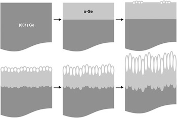
It has been well established that Ge undergoes a crystalline to amorphous phase transformation as a result of ion beam modification.Reference Claeys, Simoen, Opsomer, Brunco and Meuris40–Reference Koffel, Scheiblin, Claverie and Benassayag43 This amorphization process is accepted to be the result of an accumulation of a critical concentration of point defects resulting from ion beam modification such that the material experiences a first-order crystalline to amorphous phase transformation. In the case of single-crystal Ge with a free surface ion beam-modified at room temperature with relatively heavy ions (Ge+, e.g.,) amorphization is known to occur for ion doses greater than 5.0 × 1013 cm−2.Reference Claeys, Simoen, Opsomer, Brunco and Meuris40–Reference Birtcher44 If the ion dose is further increased, the material will remain amorphous up to a dose of ∼2.0 × 1015 cm−2, but if the dose is increased just beyond this, the material will start to structurally decompose and exhibit “pore clusters,” which nucleate at the free surface of the material.Reference Darby, Yates, Rudawski, Jones, Kontos and Elliman25 It is important to note that the crystalline to amorphous transition appears to be necessary prior to the occurrence of nanostructuring; in other words, the material must first exhibit a bulk amorphous structure prior to any pore nucleation, though it is not understood why this is the case. If the dose is further increased, the pores (also interchangeably referred to as “voids” or “craters”) completely cover and rupture the surface while becoming larger and somewhat elongated along the direction of the incident ions, generating a layer with the nanostructured morphology on top of a nonporous α-Ge layer.Reference Wilson21, Reference Romano, Impellizzeri, Tomasello, Giannazzo, Spinella and Grimaldi24–Reference Romano, Impellizzeri, Bosco, Ruffino, Miritello and Grimaldi28 As the dose further increases, the nanostructured layer experiences a large out-of-plane expansion with the individual pores continuing to elongate and the surface experiencing increased roughening;Reference Romano, Impellizzeri, Tomasello, Giannazzo, Spinella and Grimaldi24, Reference Darby, Yates, Rudawski, Jones, Kontos and Elliman25 an underlying α-Ge layer remains under the nanostructured layer, but while the thickness of the nanostructured layer continues to increase with increasing dose, the thickness of the underlying α-Ge layer remains relatively constant. This complete morphological evolution of Ge with increasing ion dose is presented schematically in Fig. 2.
Schematic representation of the microstructural evolution of Ge with increasing ion dose; the starting material is single crystal Ge, but with increasing dose an amorphous layer is formed; as the dose increases further, small clusters of near-surface pores nucleate; as the dose increases further, the pores cover the whole surface and elongate into the wafer, forming the nanostructured morphology; as the dose increases further, the pores elongate further and the material experiences a large out-of-plane expansion with the nanostructured region existing on top of a nonporous amorphous layer. In all cases, the surface roughness and roughness of the amorphous/crystalline interface increase with increasing ion dose.

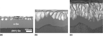
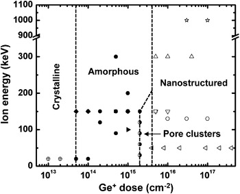
Likewise, Figs. 3(a)–3(c) present XTEM images of nanostructured Ge prepared by Ge+-implantation at 130 keV at room temperature to doses of 1.0 × 10¹⁶, 3.0 × 10¹⁶, and 1.0 × 1017 cm−2. The evolution of the pore size and morphology as well as the thickness of the nanostructured layer with increasing ion dose is clearly evident as described previously. Additionally, a “damage map” adapted from Darby et al.Reference Darby, Yates, Rudawski, Jones, Kontos and Elliman25 displays the relationship between incident ion energy, dose, and resulting microstructure for Ge+-implantation at room temperature into single-crystal Ge as presented in Fig. 4; it is evident that ion dose is the primary factor that controls morphological evolution. In addition to this qualitative observation of the morphological evolution, work regarding the quantification of the nanostructured morphology as a function of ion beam modification conditions has also been performed as will be discussed in detail in a subsequent section.
XTEM images showing the morphological evolution of nanostructuring in Ge with increasing ion dose as a result of Ge+-implantation at 130 keV at room temperature into single-crystal (001) Ge: (a) 1.0 × 10¹⁶, (b) 3.0 × 10¹⁶, and (c) 1.0 ×1017 cm−2 ion doses. Reproduced and modified with permission from Darby et al.Reference Darby, Yates, Rudawski, Jones, Kontos and Elliman25 Copyright © 2011 by Elsevier. Reprinted by permission of Elsevier.

The dose-dependence of the morphological evolution is the most well known aspect of nanostructuring in Ge due to ion beam modification. However, the process is also known to be sensitive to the substrate temperatureReference Appleton, Holland, Narayan, Schow, Williams, Short and Lawson20, Reference Stritzker, Elliman and Zou27, Reference Glover, Ridgway, Byrne, Yu, Foran, Clerc, Hansen and Larsen29, Reference Ridgway, Glover, Yu, Foran, Clerc, Hansen and Larsen30, Reference Rudawski, Yates, Holzworth, Jones, Elliman and Volinsky45 maintained during ion beam modification as well as the nature of the material prior to ion beam modification;Reference Romano, Impellizzeri, Bosco, Ruffino, Miritello and Grimaldi28, Reference Yates, Darby, Elliman and Jones31, Reference Rudawski, Darby, Yates, Jones, Elliman and Volinsky46 both of these factors will be discussed in detail in subsequent sections of this review. These basic considerations noted, finer details regarding quantification of the nanostructured morphology, the role of temperature during implantation, the influence of the starting material microstructure, and the implications of the empirical observations for the proposed formation mechanisms will be presented.
III. “TEMPERATURE WINDOW” FOR NANOSTRUCTURING
As stated previously, the temperature at which ion beam modification is performed has a profound influence on the nanostructuring process. It was first revealed by Appleton et al.Reference Appleton, Holland, Narayan, Schow, Williams, Short and Lawson20 using XTEM that by performing ion beam modification at temperature T = −196 °C it was possible to suppress nanostructuring in initially single-crystal Ge. Shortly after, work by Holland et al.Reference Holland, Appleton and Narayan22 confirmed this observation, but also produced the interesting result that nanostructuring was suppressed when T > 300 °C. More than two decades later, work by Ottaviano et al.Reference Ottaviano, Verna, Grossi, Parisse, Piperno, Passacantando, Impellizzeri and Priolo34 also investigated the role of specimen temperature during ion beam modification on resulting morphology using top-down SEM, but revealed that nanostructuring was suppressed when T > 240 °C, which is a discrepancy of ∼60 °C as compared with the result of Holland et al.Reference Holland, Appleton and Narayan22 To date, the most complete study on the temperature influence on nanostructuring in Ge due to ion beam modification can be credited to Strizker et al.Reference Stritzker, Elliman and Zou27 who used XTEM to investigate the resulting material morphology as a function of temperature during ion beam modification for a wide temperature range over relatively fine temperature increments and determined that a “temperature window” for nanostructuring existed for—80 ≤ T ≤ 200 °C. Additionally, recent work by Rudawski et al.Reference Rudawski, Yates, Holzworth, Jones, Elliman and Volinsky45 revealed that nanostructuring was suppressed for ion beam modification at T = – 196 °C into an as-deposited amorphous Ge film as shown in Fig. 5, so the effect appears to be somewhat independent of starting material structure. It is also noteworthy that when the temperature is above the upper range of temperature window, the material never experiences amorphization or nanostructuring during ion beam modificationReference Holland, Appleton and Narayan22; this is consistent with the findings presented in Fig. 4 showing that it is necessary for the material to be become amorphous during ion beam modification (or be amorphous prior to ion beam modification) for nanostructuring to occur.
Implant “damage map” showing the resultant microstructure of Ge as a function of Ge+ ion energy and dose at room temperature (initially single crystal material); the sources for each reported data point are specified elsewhere.Reference Darby, Yates, Rudawski, Jones, Kontos and Elliman25 Reproduced and modified with permission from Darby et al.Reference Darby, Yates, Rudawski, Jones, Kontos and Elliman25 Copyright © 2011 by Elsevier. Reprinted by permission of Elsevier.

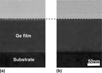
XTEM images of an as-deposited amorphous Ge film on a metallic substrate: (a) as-deposited and (b) after Ge+-implantation at 260 keV to a dose of 1.0 × 1016 cm−2 at T = −196 °C showing that nanostructuring can be suppressed when ion beam modification is performed outside the so-called “temperature window” (surface indicated by dotted line). Reproduced and modified with permission from Rudawski et al.Reference Rudawski, Yates, Holzworth, Jones, Elliman and Volinsky45 Copyright © 2013 by Elsevier. Reprinted by permission of Elsevier.

It is evident that among the work that investigated the upper range of the temperature window for nanostructuring there appears to be some discrepancies in the upper limit to suppress nanostructuring.Reference Holland, Appleton and Narayan22, Reference Stritzker, Elliman and Zou27, Reference Ottaviano, Verna, Grossi, Parisse, Piperno, Passacantando, Impellizzeri and Priolo34 Perhaps a difference in the energy regimes used for ion beam modification in each study may have been a causal factor, as the work of Holland et al.Reference Holland, Appleton and Narayan22 and Ottaviano et al.Reference Ottaviano, Verna, Grossi, Parisse, Piperno, Passacantando, Impellizzeri and Priolo34 used ion energies of the order of hundreds of keV while the work of Strizker et al.Reference Stritzker, Elliman and Zou27 used energies of 1 MeV. Yet, considering the similar nature of the former two studies, it is still somewhat unclear why there would be a discrepancy to the extent of 60 °C for the upper temperature limit for nanostructuring. In any case, the presence of a temperature window for nanostructuring due to ion beam modification indicates that competing thermally activated process may play a role in the fundamental formation mechanism; this temperature window will be revisited subsequently when the implications of experimental observations for proposed mechanisms are discussed.
IV. MORPHOLOGICAL QUANTIFICATION
Whereas structural decomposition of Ge due to ion beam modification has been studied for several decades, relatively little work has focused on quantification of the nanostructured morphology with most studies having been predisposed towards qualitative observations. In this section, the many attempts to quantify the nanostructured morphology are reviewed. Using the treatment of Romano et al.,Reference Romano, Impellizzeri, Tomasello, Giannazzo, Spinella and Grimaldi24 the features of the nanostructured morphology that are discussed are the pore radius (R) distribution and areal pore density (Q) as viewed in top-down orientation, the thickness of the nanostructured layer (h) when viewed in cross-sectional orientation, the out-of-plane swelling (s) as measured relative to the position of the virgin surface prior to ion beam modification, and surface roughness.
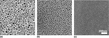
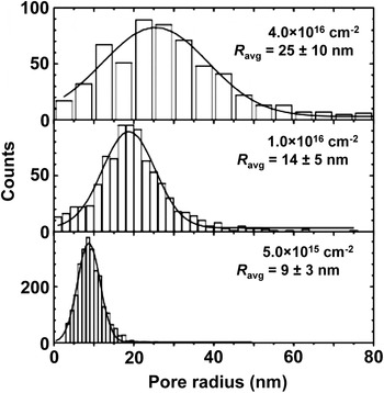
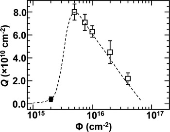
The first attempt at quantification of the changes in microstructure in Ge due to ion beam modification should probably be credited to Wilson et al.,Reference Wilson21 who used top-down SEM to investigate the average pore radius (R avg) as a function of ion dose (Φ) for a given ion energy and revealed that R avg increases with increasing dose until somewhat of a saturation point is reached. Later work by Ottaviano et al.Reference Ottaviano, Verna, Grossi, Parisse, Piperno, Passacantando, Impellizzeri and Priolo34 and Romano et al.Reference Romano, Impellizzeri, Tomasello, Giannazzo, Spinella and Grimaldi24, Reference Romano, Impellizzeri, Bosco, Ruffino, Miritello and Grimaldi28 also used top-down SEM to quantify the R distribution. The results from Romano et al.Reference Romano, Impellizzeri, Tomasello, Giannazzo, Spinella and Grimaldi24, Reference Romano, Impellizzeri, Bosco, Ruffino, Miritello and Grimaldi28 largely confirm what Wilson et al.Reference Wilson21 first quantified roughly three decades earlier; some of these findings are presented in Figs. 6(a)–6(c), which present top-down SEM images of nanostructured Ge prepared by Ge+-implantation at 300 keV at room temperature to doses of 5.0 × 10¹⁵, 1.0 × 10¹⁶, and 4.0 × 1016 cm−2, respectively. Figure 7 shows the quantified R distributions for each of these doses and confirms that R avg increases with dose. The work of Ottaviano et al.Reference Ottaviano, Verna, Grossi, Parisse, Piperno, Passacantando, Impellizzeri and Priolo34 also produced the interesting result that R tended to decrease with increasing substrate temperature during ion beam modification and nanostructuring. In both cases, an inverse relationship between R avg and Q was demonstrated and is evident from Fig. 5.Reference Romano, Impellizzeri, Tomasello, Giannazzo, Spinella and Grimaldi24, Reference Romano, Impellizzeri, Bosco, Ruffino, Miritello and Grimaldi28, Reference Ottaviano, Verna, Grossi, Parisse, Piperno, Passacantando, Impellizzeri and Priolo34 Additionally, Romano et al. quantified Q as a function of ion dose for Ge+-implantation at 300 keV at room temperature into single-crystal Ge for ion doses ≥5.0 × 1015 cm−2 and confirmed this relationship as presented in Fig. 8. However, Darby et al.Reference Darby, Yates, Rudawski, Jones, Kontos and Elliman25 used plan-view TEM and measured R avg = 8 ± 3 nm and Q = 4.0 × 10⁹ for Ge+-implantation at 90 keV at room temperature to a dose of 2.0 × 1015 cm−2. Whereas the value of ion energy is not the same as that used by Romano et al.,Reference Romano, Impellizzeri, Tomasello, Giannazzo, Spinella and Grimaldi24 it is interesting that this value for R avg is consistent with the trend observed in Fig. 7 in that R avg tends to increase with ion dose. However, the value of Q is not consistent with that reported in Fig. 7 in that it is actually smaller for a lower dose. Thus, if the Q versus ion dose data were collected for a larger dose range, it may actually obey the trend indicated by the continuous line superimposed on Fig. 8 where a maximum in the curve may be observable at some particular dose.
Top-down SEM images of nanostructured Ge prepared by Ge+-implantation at 300 keV into (001) Ge to doses of (a) 5.0 × 10¹⁵, (b) 1.0 × 10¹⁶, and (c) 4.0 × 1016 cm−2. Reproduced and modified with permission from Romano et al.Reference Romano, Impellizzeri, Tomasello, Giannazzo, Spinella and Grimaldi24 Copyright © 2010 by the American Institute of Physics. Reprinted by permission of the American Institute of Physics.

Pore radius distribution of nanostructured Ge prepared by Ge+-implantation at 300 keV into single-crystal (001) Ge for doses of 5.0 × 10¹⁵, 1.0 × 10¹⁶, and 4.0 × 1016 cm−2 as measured by top-down SEM; the average pore radius (R avg) for each dose is indicated. Reproduced and modified with permission from Romano et al.Reference Romano, Impellizzeri, Tomasello, Giannazzo, Spinella and Grimaldi24 Copyright © 2010 by the American Institute of Physics. Reprinted by permission of the American Institute of Physics.

Areal pore density as a function of ion dose for nanostructured Ge prepared by Ge+-implantation at room temperature into single-crystal Ge as reported by Romano et al.Reference Romano, Impellizzeri, Tomasello, Giannazzo, Spinella and Grimaldi24 for an ion energy of 300 keV (?) and Darby et al.Reference Darby, Yates, Rudawski, Jones, Kontos and Elliman25 for an ion energy of 90 keV (?); the dotted line indicates the general trend of the data and does not correspond to the fit of any model.

Of course, as stated earlier, the pores tend to evolve in an elongated fashion as the ion dose is increased (at least when the starting material is single crystal), which results in an increase in h with increasing dose; this increase in h with ion dose is related to the macroscopic out-of-plane swelling, s, but is not exactly the same as will be discussed shortly. Romano et al.Reference Romano, Impellizzeri, Tomasello, Giannazzo, Spinella and Grimaldi24 were the first to quantify h using several different cross-sectional approaches including cross-sectional SEM and XTEM. Using an argument that the total volume of the pores was equivalent to the total amount of excess vacancies, it was ultimately revealed that h obeyed the following relationship:
 $$ \pi QR_{avg}^2 h = {{n_{vac} } \over {\rho _{Ge} }}(\Phi - \Phi _0 )\quad, $$
where nvac is the number of vacancies created per incident ion as predicted by simulations,Reference Ziegler47ρ Ge is the density of Ge, Φ is the ion dose, and Φ0 is the threshold dose for nanostructuring; the total volume of the pores per unit surface area is thus  $\pi QR_{avg}^2 h$ and is expected to increase linearly with dose, which was consistent with observations.Reference Romano, Impellizzeri, Tomasello, Giannazzo, Spinella and Grimaldi24
Of course, it should be noted that h and s, while clearly related, are actually different as h is the thickness of the nanostructured layer whereas s is the swelling relative to the virgin surface position; in fact, it was not until relatively recently that the difference between h and s was actually delineated through careful measurement.Reference Romano, Impellizzeri, Tomasello, Giannazzo, Spinella and Grimaldi24 Prior to this, researchers were quantifying the change in surface position relative to the virgin surface location, which of course is s, though it was thought at times that the amount of swelling was indicative of the total thickness of material that had been rendered nanostructured, which is h. Huber et al.Reference Huber, Assmann, Karamian, Mucklich, Prusseit, Gazis, Grotzschel, Kokkoris, Kossionidis, Mieskes and Vlastou33 first quantified s a function of ion dose for different incident ion energies in the range of a few hundred MeV using atomic force microscopy (AFM). It was determined that s could be modeled after Prins et al.Reference Prins, Derry and Sellschop48 as
 $$s = s_{\max } \left[ {1 - e^{ - (a\Phi + b)} } \right]\quad,$$
where s max is the maximum out-of-plane swelling, a is a constant with units of cm2 i.e., related to the number of vacancies produced per incident ion, and b is pure fitting constant. The parameters s max, a, and b all depend on the incident ion mass and energy; specifically, it was shown that all three increase with increasing ion energy.Reference Huber, Assmann, Karamian, Mucklich, Prusseit, Gazis, Grotzschel, Kokkoris, Kossionidis, Mieskes and Vlastou33 Work by Strizker et al.Reference Stritzker, Elliman and Zou27 also quantified s as function of ion dose at ion energies of the order of a few MeV using XTEM and produced results that qualitatively agreed with those of Huber et al.Reference Huber, Assmann, Karamian, Mucklich, Prusseit, Gazis, Grotzschel, Kokkoris, Kossionidis, Mieskes and Vlastou33 but tended to show a linear relationship between s and ion dose. Work several years later by Steinbach et al.Reference Steinbach, Wernecke, Kluth, Ridgway and Wesch49 also produced similar results showing a linear relationship between s and ion dose, but at ion energies of the order of a few hundred MeV, which again contradicts the findings of Huber et al.Reference Huber, Assmann, Karamian, Mucklich, Prusseit, Gazis, Grotzschel, Kokkoris, Kossionidis, Mieskes and Vlastou33
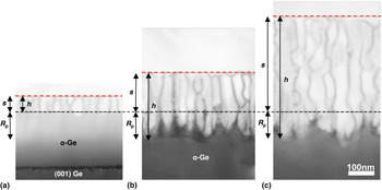
More recently, Romano et al.Reference Romano, Impellizzeri, Tomasello, Giannazzo, Spinella and Grimaldi24 also quantified s using AFM, but at ion energies of the order of a few hundred keV. In similarity to the results from the three previously studies, an increase in s with ion dose was revealed. However, the s-ion dose relationship did not appear to obey the relationship advanced by Huber et al.Reference Huber, Assmann, Karamian, Mucklich, Prusseit, Gazis, Grotzschel, Kokkoris, Kossionidis, Mieskes and Vlastou33 using Eq. (2) or the linear relationship of Strizker et al.Reference Stritzker, Elliman and Zou27 and Steinbach et al.Reference Steinbach, Wernecke, Kluth, Ridgway and Wesch49 Rather, s tended to increase exponentially with ion dose. The difference between the results of Romano et al.Reference Romano, Impellizzeri, Tomasello, Giannazzo, Spinella and Grimaldi24 and the other three studies may be due to the ion energies used in each study. Specifically, the former used ion energies of the order of a few hundred keV whereas the later used ion energies of the order of a few to a few hundred MeV; therefore the ion energy regime may play a role in the evolution of s with ion dose. Although, the issue of why some have shown a swelling-ion dose relationship for the ion energy regime of a few to a few hundred MeV consistent with Eq. (2) and others have shown a linear relationship for the same energy regime remains unclear. More importantly, Romano et al.Reference Romano, Impellizzeri, Tomasello, Giannazzo, Spinella and Grimaldi24 were able to delineate the difference between h and s via the use of both AFM and XTEM. Specifically, it was shown that the following relationships govern the relationship between h, s, and the projected range of the ions (R p):
 $$h = s\,\left( {s \,\,\le \,\,R_p } \right)\quad,$$
and
 $$h = s + R_p \,\left( {s > R_p } \right)\quad.$$
Thus, the nanostructured layer thickness is never smaller than the out-of-plane swelling, but when the amount of swelling is much larger than R p (e.g., when the ion energy is relatively low) h is nearly equal to s. Figures 9(a)–9(c) present XTEM images of nanostructured Ge prepared by Ge+-implantation at 300 keV to doses of 1.0 × 10¹⁶, 2.0 × 10¹⁶, and 4.0 × 1016 cm−2; the evolution of h and s as predicted by Eq. (3) is clearly evident.
XTEM images showing the out-of-plane swelling (s) and nanostructured layer height (h) for Ge+-implantation at 300 keV to doses of: (a) 1.0 × 10¹⁶, (b) 2.0 × 10¹⁶, and (c) 4.0 × 1016 cm−2. The black dotted line indicates the initial position of the specimen surface prior to ion beam modification whereas the red line indicates the actual specimen surface; the projected range (R p) of the incident ions relative to the initial surface position is also indicated. Reproduced and modified with permission from Romano et al.Reference Romano, Impellizzeri, Tomasello, Giannazzo, Spinella and Grimaldi24 Copyright © 2010 by the American Institute of Physics. Reprinted by permission of the American Institute of Physics.

As evidenced in Fig. 3, it is clear that there tends to be surface roughening resulting from ion beam modification-induced structural decomposition. Several studies have shown that the surface roughness does increase as a result of ion beam modification-induced nanostructuring;Reference Romano, Impellizzeri, Tomasello, Giannazzo, Spinella and Grimaldi24, Reference Ottaviano, Verna, Grossi, Parisse, Piperno, Passacantando, Impellizzeri and Priolo34, Reference Janssens, Huyghebaert, Vanhaeren, Winderickx, Satta, Meuris and Vandervorst50–Reference Kim, Cahill and Averback52 however, relatively few studies have characterized this surface roughening as a function of ion beam modification conditions. Chen et al.Reference Chen, Wilson, Cheung, Xu and Wong32 were the first to quantify surface roughening as a result of ion beam modification-induced nanostructuring using AFM and revealed that the surface roughness increased approximately linearly with ion dose whereas the surface roughness tended to increase with decreasing ion energy for a given ion dose; additional work also investigated the role of beam current density during ion beam modification on surface roughness, but did not indicate a very large effect. Later work by Kaiser et al.Reference Kaiser, Koffel, Pichler, Bauer, Amon, Claverie, Benassayag, Scheiblin, Frey and Ryssel26 also quantified the surface roughening associated with formation of the nanostructured morphology as a function of ion dose for several different ion masses and ion energies using AFM. In general, it was shown that the surface roughness tended to increase with increasing dose for a given ion mass and energy; however, the roughness tended to increase with ion energy for a given ion dose, which is somewhat contradictory in relation to the earlier results of Chen et al.Reference Chen, Wilson, Cheung, Xu and Wong32 More interestingly, the same work by Kaiser et al.Reference Kaiser, Koffel, Pichler, Bauer, Amon, Claverie, Benassayag, Scheiblin, Frey and Ryssel26 revealed that there is also some dependence of surface roughness on dose rate, with roughness observed to increase with dose rate for a given ion dose and energy, which again somewhat contradicts Chen et al.Reference Chen, Wilson, Cheung, Xu and Wong32 The discrepancy between Chen et al.Reference Chen, Wilson, Cheung, Xu and Wong32 and Kaiser et al.Reference Kaiser, Koffel, Pichler, Bauer, Amon, Claverie, Benassayag, Scheiblin, Frey and Ryssel26 may once again be due to the range of ion energies used in each study as the former investigated ion energies of the order of tens of keV whereas the later investigated energies of the order of a few hundred keV; presumably the dose rate effect then only becomes noticeable at high ion energies.
Summarizing the prior work on quantifying the nanostructured morphology, the main considerations have focused on the pore radius distribution, the thickness of the nanostructured layer, the out-of-plane swelling, and the surface roughness. These efforts are noteworthy, not only because of the importance for potential applications of the nanostructured morphology, but also for the implications for the proposed formation mechanisms as will be revisited later.
V. INFLUENCE OF STARTING MATERIAL
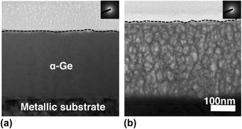
The vast majority of reported work studying the macroscopic considerations of nanostructuring of Ge via ion beam modification utilized single crystals for the initial material. However, as first shown by Peto et al.Reference Peto, Horvath, Gereben, Pusztai, Hajdu and Svab53 it has been demonstrated that the starting material does not need to be crystalline for nanostructuring to occur. Specifically, nanostructuring has been demonstrated to occur in amorphous Ge films prepared via electron beam evaporation,Reference Rudawski, Darby, Yates, Jones, Elliman and Volinsky46 as well as sputter deposition,Reference Romano, Impellizzeri, Bosco, Ruffino, Miritello and Grimaldi28, Reference Yates, Darby, Elliman and Jones31, Reference Peto, Horvath, Gereben, Pusztai, Hajdu and Svab53 and molecular beam epitaxy (MBE),Reference Impellizzeri, Romano, Bosco, Spinella and Grimaldi54 and also in starting material that was initially polycrystalline.Reference Impellizzeri, Romano, Bosco, Spinella and Grimaldi54 In the case of material that was initially polycrystalline, the material exhibited a transition to a bulk amorphous morphology prior to nanostructuring, in similarity to the case of initially single-crystal material.Reference Impellizzeri, Romano, Bosco, Spinella and Grimaldi54Figure 10 presents XTEM images showing as-deposited amorphous Ge becoming nanostructured as a result of Ge+-implantation at 260 keV at room temperature to a dose of 1.0 × 1016 cm−2. More curiously, it has been demonstrated that the nature of the starting material plays a role in the final morphology of the material following ion beam modification.
XTEM images showing that ion beam modification-induced nanostructuring can also occur in initially amorphous Ge: (a) an as-deposited amorphous Ge film on a metallic substrate and (b) the same film after Ge+-implantation at 260 keV to a dose of 1.0 × 1016 cm−2. Reproduced and modified with permission from Rudawski et al.Reference Rudawski, Darby, Yates, Jones, Elliman and Volinsky46 Copyright © 2012 by the American Institute of Physics. Reprinted by permission of the American Institute of Physics.

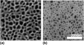
Romano et al.Reference Romano, Impellizzeri, Bosco, Ruffino, Miritello and Grimaldi28 were the first to show qualitatively and quantitatively the differences between nanostructured Ge formed via ion beam modification with initial single-crystal or as-deposited amorphous starting material. Specifically, it was shown that the as-deposited amorphous material did not exhibit the elongated pore structure that was observed in the case of single-crystal starting material. Additionally, the thickness of the material that was rendered nanostructured was approximately twice as great for the case of the as-deposited amorphous Ge material as compared with the single-crystal material; Figs. 11(a) and 11(b) present top-down SEM images of nanostructured Ge prepared from single-crystal (001) and amorphous Ge deposited via MBE by Ge+-implantation at 300 keV at room temperature to a dose of 1.0 × 1016 cm−2; it is evident that the average pore radius is much larger for the case of single-crystal (001) Ge when compared with as-deposited amorphous Ge. Work by Impellizzeri et al.Reference Impellizzeri, Romano, Bosco, Spinella and Grimaldi54 compared polycrystalline versus amorphous starting material prepared by MBE and produced results similar to that of Romano et al.Reference Romano, Impellizzeri, Bosco, Ruffino, Miritello and Grimaldi28 in that the nanostructured material produced from initially polycrystalline material exhibited more elongated and larger average pore radius as compared with the nanostructured material produced from as-deposited amorphous material. Ultimately, both Romano et al.Reference Romano, Impellizzeri, Bosco, Ruffino, Miritello and Grimaldi28 and Impellizzeri et al.Reference Impellizzeri, Romano, Bosco, Spinella and Grimaldi54 argued that the presence of small voids within the initially amorphous material (easily observed using XTEM) were possibly serving as nucleation sites for pores during ion beam-induced structural decomposition; as the inherent voiding in the single-crystal or polycrystalline material was much less than in the case of the amorphous material, the pore density would be smaller in the former two cases as compared with the latter as there were fewer sites for pore nucleation, which was exactly what was observed experimentally. More recently, work by Yates et al.Reference Yates, Darby, Elliman and Jones31 systematically investigated the influence of inherent voiding in initially amorphous material by altering the deposition conditions such that voiding of the films in the as-deposited state was different. Ultimately, results consistent with those presented by Romano et al.Reference Romano, Impellizzeri, Bosco, Ruffino, Miritello and Grimaldi28 and Impellizzeri et al.Reference Impellizzeri, Romano, Bosco, Spinella and Grimaldi54 were produced: the density of pores was greater in the material with a greater amount of voiding in the as-deposited state and the pores were not elongated as compared with the case of single-crystal starting material.
Top-down SEM images of nanostructured Ge prepared via Ge+-implantation at 300 keV to a dose of 2.0 × 1016 cm−2 from (a) as-deposited amorphous and (b) single-crystal (001) Ge. Reproduced and modified with permission from Romano et al.Reference Romano, Impellizzeri, Bosco, Ruffino, Miritello and Grimaldi28 Copyright © 2012 by the American Institute of Physics. Reprinted by permission of the American Institute of Physics.

Finally, it should be noted that some work explored the effect of “preamorphizing” a Ge single-crystal substrate and then subsequently implanting the material to induce nanostructuring.Reference Gaertner, Joehrens, Steinbach, Schnohr, Ridgway and Wesch37, Reference Steinbach, Schnohr, Kluth, Giulian, Araujo, Sprouster, Ridgway and Wesch55, Reference Wesch, Schnohr, Kluth, Hussain, Araujo, Giulian, Sprouster, Byrne and Ridgway56 However, it is unclear whether these results can be compared to the aforementioned results that used as-deposited amorphous Ge, as the cumulative effect of ion beam modification encompasses acts that both amorphize and nanostructure the material.
The results from studying generation of the nanostructured morphology using ion beam modification in initially amorphous material provide insight into the fundamental nature of the nanostructuring process. Specifically, it is evident that nucleation sites (inherent pores) appear to play an important role in the process. This observation will be returned to shortly when the different models for nanostructuring using ion beam modification are discussed.
VI. IMPLICATIONS FOR PROPOSED FORMATION MECHANISMS
To date, two different models have been advanced to explain the structural decomposition experienced by Ge as a result of ion beam modification: vacancy-clustering and microexplosions. The vacancy clustering mechanismReference Holland, Appleton and Narayan22, Reference Romano, Impellizzeri, Tomasello, Giannazzo, Spinella and Grimaldi24, Reference Ridgway, Glover, Yu, Foran, Clerc, Hansen and Larsen30, Reference Chen, Wilson, Cheung, Xu and Wong32–Reference Ottaviano, Verna, Grossi, Parisse, Piperno, Passacantando, Impellizzeri and Priolo34 is believed to result from the inefficient recombination of point defects. In the case of pure Ge, point defect recombination is inefficient to the point that a high concentration of excess vacancies in the near-surface region of the material can result from ion beam modification as predicted by simulations. As the dose of ions is increased, the concentration of excess vacancies increases to the point at which macroscopic voids form, which is the initial stage of structural decomposition. Of course, as has already been shown, it is necessary for Ge to amorphize (or be amorphous) prior to structural decomposition. It may therefore seem counterintuitive to describe the existence of vacancies in an amorphous material. However, work strongly suggests that vacancy defects do exist in amorphous elemental semiconductors as a result of ion beam modification and that these vacancies have very similar configurations comparable to those occurring in the crystalline counterparts.Reference Roorda, Sinke, Poate, Jacobson, Dierker, Dennis, Eaglesham, Spaepen and Fuoss57, Reference Vandenhoven, Liang, Niesen and Custer58 The question of the existence of vacancies in amorphous Ge due to ion beam modification notwithstanding, the main implications of the vacancy clustering model are as follows: (i) the voids should nucleate near the peak of the excess vacancies profile, (ii) the voids should nucleate in a uniform manner concomitant with the uniformity of the ion beam modification process, (iii) the total volume of voided material should increase with increasing ion dose, (iv) as vacancy motion and generation/annihilation and the crystalline to amorphous transition are thermally activated processes, nanostructuring should be sensitive to temperature during ion beam modification, and (v) the evolution of the microstructure should exhibit a ripening-like process as it would be energetically favorable for smaller pores to dissolve at the expensive of the growth of larger pores.
The microexplosion theory of nanostructuring due to ion beam modification is fundamentally different from the vacancy-clustering model.Reference Bellon, Chey, Vannostrand, Ghaly, Cahill and Averback36–Reference Mayr and Averback39 The theory of microexplosions holds that near-surface voids are created through pressure waves caused by the overlap of ion cascades; each void is therefore the result of a microexplosion with only ∼0.1% of all incident ions expected to produce microexplosions. Whereas the vacancy-clustering model depends primarily on inefficiency of point defect recombination, the ability of a material to experience microexplosions during ion beam modification is dependent on ion mass/energy, bond strength, melting temperature, atomic density, and average atomic mass.Reference Ghaly, Nordlund and Averback38 In terms of predictive implications that may be compared with experimental results, the microexplosion mechanism holds that (i) pores should always form near the surface regardless of incident ion energy, (ii) that the number of voids formed should always be ∼0.1% of the total ion dose, and (iii) the process should be independent of specimen temperature during ion beam modification as all the controlling factors are independent (or nearly independent) of temperature.
First considering the structural evolution of the nanostructured morphology with ion dose as previously described, it appears both models can explain the increase in porosity with increasing dose. However, the changes in pore morphology with ion dose as well as the observed temperature window are reasonably described only via vacancy clustering, as microexplosions are not associated with the formation, migration, and annihilation of any point defect. That being said, in the case of initially single-crystal Ge, it has been clearly and independently demonstrated that pores always nucleate at the free surface of the material and not at the peak of the expected vacancy concentration profile, which actually supports the microexplosion rather than vacancy-clustering approach. Furthermore, it was demonstrated by Darby et al.Reference Darby, Yates, Rudawski, Jones, Kontos and Elliman25 in the case of initially single-crystal material that the pores tend to nucleate in clusters, rather than in a uniform manner, which is not predicted by vacancy-clustering or microexplosions mechanisms.
Of course, as shown earlier, when the material prior to ion beam modification is amorphous, the nanostructuring process evolves quite differently as compared with when the material is initially single-crystal or polycrystalline. Specifically, pores initially present in the material appear to serve as nucleation sites for further structural decomposition during ion beam modification. Additionally, the nucleation of the pores did not appear to commence at the specimen surface, but more closely near the predicted peak of the vacancy concentration profile.Reference Yates, Darby, Elliman and Jones31 If it is therefore assumed that some sort of nucleation site is needed for macroscopic pore formation (regardless of the nature of the starting material), a more complete picture of the mechanism of nanostructuring due to ion beam modification can be produced.
In the case of initially single- or polycrystalline material, which is reasonably assumed to lack the inherent pores present in as-deposited amorphous Ge, amorphization followed by the generation of some sort of nucleation site are first needed. Perhaps then, a pore formed via a microexplosion in amorphized material serves as a nucleation site in this case, as first advanced by Darby et al.Reference Darby, Yates, Rudawski, Jones, Kontos and Elliman25 This would explain why initial pore formation in initially crystalline material occurs only at the surface (as predicted by the microexplosions mechanism). However, the areal pore density values for a given ion dose are at least two orders of magnitude lower than predicted by the microexplosions mechanism as shown in Fig. 8 and the pores tend to nucleate in clusters rather than uniformly as shown by Darby et al.,Reference Darby, Yates, Rudawski, Jones, Kontos and Elliman25 which contradicts both mechanisms. Thus, it may be in the case of initially crystalline material that a dual mechanism is responsible for nanostructuring. Specifically, a microexplosion produces a near-surface pore which serves as a nucleation point for vacancies formed during ion beam modification to cluster into additional pores; as the number of pores increases, it becomes energetically favorable for the pores to coalesce into larger pores. If the temperature of the specimen is below the temperature window for nanostructuring, vacancy clustering around the pores produced by microexplosions is suppressed. Conversely, if the temperature of the specimen is above the temperature window, the material never amorphizes and therefore cannot ever structurally decompose during ion beam modification. Of course, if the generation of microexplosions is independent of temperature, it should be possible to observe microexplosions experimentally regardless of specimen temperature during ion beam modification. However, due to the near submicroscopic nature, it is difficult in practice to experimentally observe microexplosions, especially via the use of TEM, which is critical in the characterization of the nanostructured morphology.
The consistent nucleation of the pores near the surface in initially single- or polycrystalline material is perhaps the strongest evidence in support of the microexplosions mechanism playing a role in the nanostructuring process. However, if there is any preferential diffusion of vacancies to the surface, as has been suggested to be the case in elemental semiconductors,Reference Lim, Rafferty and Klemens59 this observation may actually support the vacancy-clustering mechanism. If i.e., the case, then surface nucleation will occur as a result of the accumulation of vacancies, so it is therefore no longer necessary to invoke the use of a microexplosion to serve as a nucleation site for the generation of a pore in the case of initially single- or polycrystalline material.
In the case of initially amorphous material, there is no need for microexplosions to occur to serve as nucleation sites as inherent pores already serve as such sites, so the process should be entirely controlled by vacancy-clustering. Thus, the pores should nucleate in a uniform manner over the specimen surface and at the depth in the specimen where vacancy generation is greatest, which is consistent with observations. Also, nanostructuring should still be sensitive to the temperature window and exhibit ripening with increasing dose, which again are both consistent with experimental observations.
Thus, summarizing the experimental observations and the implications for the two proposed formation mechanisms, both may play roles depending on whether the material is initially crystalline or amorphous prior to ion beam modification. Of course, what is still not clear in either case is why the material must be amorphous prior to structural decomposition, either in the virgin state or as an intermediate state during ion beam modification.
VII. APPLICATIONS OF THE NANOSTRUCTURED MORPHOLOGY
Due to the unique morphology and relative ease of fabrication, nanostructured Ge prepared via ion beam modification has potential application in a variety of technologically relevant situations. Herein below, two of the potential applications that have shown preliminary promise are discussed: chemical sensors and energy storage.
Recent work by Impellizzeri et al.Reference Impellizzeri, Romano, Fraboni, Scavetta, Ruffino, Bongiorno, Privitera and Grimaldi60 studied the electrical properties of nanostructured Ge and revealed that the nanostructured morphology has unusually high electrical conductivity as compared with the crystalline and nonporous amorphous counterparts. In conjunction with the very large surface area to volume ratio, this makes the nanostructured morphology attractive for a variety of applications. In particular, it was suggested by Impellizzeri et al.Reference Impellizzeri, Romano, Fraboni, Scavetta, Ruffino, Bongiorno, Privitera and Grimaldi60 that the nanostructured morphology would be of potential interest in sensor applications as it was demonstrated that the material could serve as a viable template for deposition of functionalized gold (Au) nanoparticles as shown in the XTEM image presented in Fig. 12; this is significant, because it is known that the such Au nanoparticles form the basis for several different types of chemical sensors.Reference Wohltjen and Snow61
XTEM image of Au nanoparticle-decorated nanostructured Ge prepared by a combination of ion beam modification (to effect nanostructuring) with subsequent electrochemical deposition (to effect Au nanoparticle decoration); this structure has potential for use in chemical sensing applications via the use of functionalized Au nanoparticles. Reproduced and modified with permission from Impellizzeri et al.Reference Impellizzeri, Romano, Fraboni, Scavetta, Ruffino, Bongiorno, Privitera and Grimaldi60 Copyright © 2012 by the Institute of Physics. Reprinted by permission of the Institute of Physics.

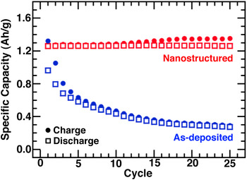
Additionally, nanostructured Ge may have potential for use in energy storage applications. Specifically, Ge is highly attractive as a rechargeable Li ion battery (LIB) anode, as it has a theoretical specific capacity i.e., ∼4.4 times that of the traditional graphite anodeReference Sangster and Pelton62 and a very high Li+ diffusivity.Reference Fuller and Severiens63 However, the main challenge associated with using Ge as an LIB electrode is accommodating the large volumetric changesReference Sangster and Pelton62 associated with electrochemical cycling of Ge with Li; the large volumetric changes tend to cause intramaterial fracture, which leads to fading of the capacity of the electrode with prolonged electrochemical cycling.Reference Huggins and Nix64 In principle, this challenge can be overcome by use of the nanostructured morphology, as it has very small characteristic feature sizes, which should be able to withstand large volumetric changes without decrepitation.Reference Arico, Bruce, Scrosati, Tarascon and Van Schalkwijk2, Reference Bruce, Scrosati and Tarascon5 Additionally, the large surface area to volume ratio should also facilitate faster insertion and extraction of Li, which should allow for faster charging and discharging of the electrode.Reference Arico, Bruce, Scrosati, Tarascon and Van Schalkwijk2, Reference Bruce, Scrosati and Tarascon5 In fact, the feasibility of nanostructured Ge as a LIB electrode was recently demonstrated by Rudawski et al.,Reference Rudawski, Darby, Yates, Jones, Elliman and Volinsky46 who showed that nanostructured Ge electrodes can withstand a large number of electrochemical cycles at a variety of cycling rate with virtually no fade in specific capacity. This is shown in Fig. 13, which presents the cycle life behavior of a nanostructured Ge electrode as compared with an as-deposited amorphous Ge electrode.
Cycle life plot of a nanostructured Ge electrode prepared by electron beam deposition of amorphous Ge on a metallic substrate followed by Ge+-implantation at 260 keV at room temperature to a dose of 1.0 × 1016 cm−2; the electrode was electrochemically cycled with metallic Li at a C/8 rate (8 h per charge or discharge); the performance of the as-deposited version of the electrode is provided to illustrate the improvement in performance resulting from nanostructuring. Reproduced and modified with permission from Rudawski et al.Reference Rudawski, Darby, Yates, Jones, Elliman and Volinsky46 Copyright © 2012 by the American Institute of Physics. Reprinted by permission of the American Institute of Physics. J

VIII. CONCLUSIONS AND FUTURE DIRECTIONS
In conclusion, the work studying nanostructuring of Ge using ion beam modification was reviewed. Specifically, the basic considerations of the morphological evolution as a function of several important variables were presented. In addition, efforts made to quantify the nanostructured morphology were also highlighted as well as the current understanding of the fundamental mechanisms governing the generation of the nanostructured morphology as well as the potential applications of nanostructured Ge with demonstrated preliminary feasibility.
Clearly, there is a relatively large amount of research that has been conducted regarding nanostructuring in Ge. However, many unanswered questions still remain. One of the most puzzling questions concerns the necessity of the material being amorphous prior to the onset of nanostructuring, as this cannot be reasonably predicted by either of the two main approaches used to explain nanostructuring. Additionally, it would be interesting to determine whether the superimposed curve for the areal pore density versus ion dose behavior indicated in Fig. 8 is consistent with observations, particularly for the relatively narrow dose range of (2.0–5.0) × 1015 cm−2 where it is expected that the pore density should actually increase with dose; verification of this predicted behavior may give further insight into whether a dual mechanism approach (microexplosions serving as nucleation sites followed by vacancy-clustering) or single mechanism approach (diffusion of vacancies to the surface with subsequent clustering) is responsible for nanostructuring in initially single- or polycrystalline material. Along these lines, the role of dose rate on morphological evolution has not been thoroughly investigated either outside of limited work where the effect on surface roughening was examined.Reference Kaiser, Koffel, Pichler, Bauer, Amon, Claverie, Benassayag, Scheiblin, Frey and Ryssel26 Additionally, the work reviewed in this article only reviewed cases where Ge with a free surface was ion beam-modified. Presumably, the morphological evolution of the nanostructured material may be quite different in cases where a solid-solid rather than solid-vacuum interface exists during ion beam modification. In particular, some initial work by Yates et al.Reference Yates, Darby, Elliman and Jones31 indicated that void nucleation does not only occur at free surfaces and any inherent voids within the material, but also at solid-solid interface. A systematic study comparing nanostructuring in Ge with different solid-solid interfaces may therefore provide greater insight into the role that nucleation sites, and particularly surfaces and interfaces, play in the nanostructuring process.
A different line of investigation that may provide further insight into the fundamental aspects of nanostructuring may be the effect of alloying. Specifically, it has been shown by Romano et al.Reference Romano, Impellizzeri, Bosco, Ruffino, Miritello and Grimaldi28 that nanostructuring was avoided in deposited amorphous silicon–germanium alloy (SiGe) films with Ge content <90 at.%. However, the role of alloying in the suppression of nanostructuring is far from unclear, though it is reasonable to expect that the addition of Si to Ge would eventually suppress nanostructuring as Si does not exhibit this behavior.Reference Davidson and Booker65–Reference Morehead and Crowder67 Of course, it would also be interesting to see if the SiGe being initially single- or polycrystalline somehow affected this apparent “concentration window” for nanostructuring. In any case, it appears there may be some fundamental difference between Ge alloyed with Si and pure Ge i.e., influencing the nanostructuring process, which is still unclear. Extensive experimental and theoretical investigations into the role of alloying on nanostructuring using ion beam modification are therefore needed. This highlights a few of the key points for further investigation into nanostructuring of Ge using ion beam modification.
ACKNOWLEDGMENTS
The authors acknowledge Luica Romano (University of Catania, Italy) for thoughtful discussions regarding this work and for agreeing to the reproduction and modification of several figures presented in this review.