Introduction
Nanotechnology allows us to fabricate novel materials and devices for applications in all disciplines in science and technology. Nanostructured materials can exhibit striking optical phenomena such as Bragg reflection, (circular) polarization, and strong enhancement of electromagnetic fields (hot spots) paving the way for highly efficient sensors and nanophotonic devices. Reference Maradudin, Sambles and Barnes1 Importantly, access to these and other intriguing physical phenomena encountered at the nanoscale offers great potential for fundamental research. Taking advantage of several methodologies such as lithography and bulk self-assembly, nanotechnology is being driven toward finding novel ways of bringing together different nanocomponents to predeterministically exploit their interactions.
For nanophotonic devices to be functional, structuring or positioning accuracy of optical components is usually required at length scales much smaller than the electromagnetic wavelength of interest. For optical wavelengths, this implies the necessity to control matter at a scale far below 50 nm. To circumvent current challenges in deterministic placement of individual functional entities, DNA has been successfully employed to arrange optical elements such as colloidal metallic nanoparticles (NPs), Reference Ding, Deng, Yan, Cabrini, Zuckermann and Bokor2 colloidal quantum dots (QDs), Reference Bui, Onodera, Kidwell, Tan, Graugnard, Kuang, Lee, Knowlton, Yurke and Hughes3 nanodiamonds, Reference Zhang, Neumann, Lindlau, Wu, Pramanik, Naydenov, Jelezko, Schüder, Huber, Huber, Stehr, Högele, Weil and Liedl4 and fluorophores Reference Stein, Steinhauer and Tinnefeld5 with nanometer precision and stoichiometric control. Reference Schreiber, Do, Roller, Zhang, Schüller, Nickels, Feldmann and Liedl6,Reference Jungmann, Avendano, Dai, Woehrstein, Agasti, Feiger, Rodal and Yin7 Over the past few years, DNA origami and other DNA self-assembling techniques have evolved as an ideal breadboard to fabricate nanophotonic structures, both static and dynamic (see the article by Wang et al. in this issue Reference Wang, Chatterjee, Yan, LaBean, Turberfield, Castro, Seelig and Ke8 ).
This article reviews the main efforts undertaken to self-assemble optical components to fabricate nanoantennas, metamaterials applications, and nanophotonic sensing devices using the DNA origami technique, and describes the main challenges that the technique is facing in those respective areas.
Optical nanoantennas
Optical antennas have been developed for nanophotonic applications to control and manipulate light at the nanoscale. Reference Novotny and van Hulst9 These antennas typically consist of an arrangement of metallic nanostructures with an optical response in the visible range associated with the excitation of localized surface plasmons. The collective oscillation of confined electrons in subwavelength-sized NPs, or localized surface plasmons, is of great interest for nanophotonic applications due to their quasiparticle nature and their ability to guide and confine light in subwavelength space. Initial fabrication efforts exploited mostly electron- and ion-beam lithography.
Despite the success of lithographically made antennas to focus light to subwavelength volumes, Reference Kinkhabwala, Yu, Fan, Avlasevich, Müllen and Moerner10 several limitations still remain. Lithographic structures are polycrystalline, which severely broadens the plasmonic resonances, compromising the performance of the optical antennas. In addition, it is difficult to fabricate structures with gaps below 10 nm. However, the main shortcoming is the challenge in coupling a single quantum emitter to an optical antenna, as this commonly involves demanding multilithographic steps to position fluorophores or QDs at the near field of the antennas. Reference Curto, Volpe, Taminiau, Kreuzer, Quidant and van Hulst11,Reference Santhosh, Bitton, Chuntonov and Haran12 An alternative approach to lithographically made antennas is the particle-on-mirror geometry, where NPs are placed on top of a metallic layer, and the spacing between them is controlled by a tunable polymer spacer. A current drawback to this approach is that it relies on undeterministic positioning of the single emitter. Reference Hill, Mock, Urzhumov, Sebba, Oldenburg, Chen, Lazarides, Chilkoti and Smith13–Reference Chikkaraddy, de Nijs, Benz, Barrow, Scherman, Rosta, Demetriadou, Fox, Hess and Baumberg17
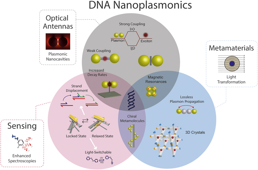
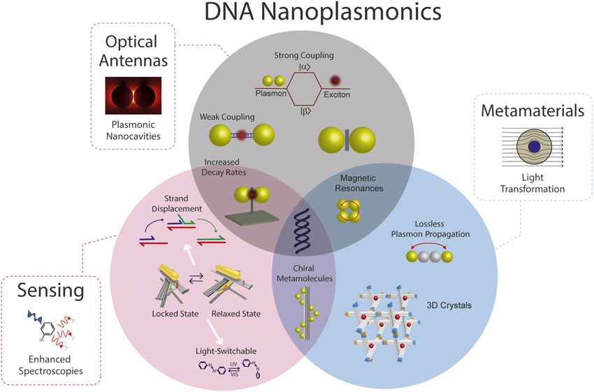
Plasmonics is the subfield of photonics that has benefited most from the versatility that DNA nanotechnology can provide ( Figure 1 , Optical Antennas panel). One advantage of using the preprogrammability of DNA is to serve as a modular template, capable of exploiting the synergy of bringing together two or more components, including colloidal NPs and single-quantum emitters. Examples include quenching of fluorophores Reference Chhabra, Sharma, Wang, Zou, Lin, Yan, Lindsay and Liu18,Reference Acuna, Bucher, Stein, Steinhauer, Kuzyk, Holzmeister, Schreiber, Moroz, Stefani, Liedl, Simmel and Tinnefeld19 and QDs Reference Samanta, Zhou, Zou, Yan and Liu20 due to nearby gold NPs and formation of molecular excitons between individual fluorophores due to proximity effects. Reference Nicoli, Roos, Hemmig, Di Antonio, de Vivie-Riedle and Liedl21
DNA as a building material for nanophotonics. DNA templates are used to assemble a great variety of nanophotonic structures that span across optical antennas (e.g., nanoparticle dimers of various sizes are used to increase fluorescence rates and enhance emissions in the weak coupling regime and to promote coherent energy exchange in the strong coupling regime), metamaterials (e.g., 3D crystals, ultrafast plasmon passage, magnetic resonances), and sensing (e.g., reconfigurable structures via strand displacement [green DNA strand displaces blue strand due to higher complementarity] or photoactivated switches [azobenzene molecules undergo conformational change upon light excitation, which can be used to dehybridize double-stranded DNA]). Note: UV, ultraviolet; VIS, visible; |α> and |β>, upper and lower energy eigenstates.
A noteworthy use of DNA is its ability to finely control the interparticle distance between colloidal metallic NPs, permitting the fabrication of plasmonic nanocavities with tailored plasmon resonance. The gap within the NPs contains a region of enhanced field, which is well below the diffraction limit, the so-called “hotspot.” In the weak coupling regime, these plasmonic nanocavities can serve as optical antennas and can be used to enhance fluorescence intensity ( Figure 2c), Reference Acuna, Moller, Holzmeister, Beater, Lalkens and Tinnefeld22–Reference Zhang, Gao, Li, Lang and Xu27 photostability, Reference Pellegrotti, Acuna, Puchkova, Holzmeister, Gietl, Lalkens, Stefani and Tinnefeld28 Raman spectroscopy signals, Reference Thacker, Herrmann, Sigle, Zhang, Liedl, Baumberg and Keyser29–Reference Prinz, Heck, Ellerik, Merk and Bald35 as well as resonance energy transfer (RET). Reference Bidault, Devilez, Ghenuche, Stout, Bonod and Wenger36,Reference Aissaoui, Moth-Poulsen, Kall, Johansson, Wilhelmsson and Albinsson37 Interactions between the single emitter and the plasmonic antennas can affect the photophysical rates Reference Holzmeister, Pibiri, Schmied, Sen, Acuna and Tinnefeld38 and mediate the emission of single quantum sources. Reference Raab, Vietz, Stefani, Acuna and Tinnefeld39 Additionally, it can increase the spontaneous emission intensity and emission rates desired for high-speed optical devices. Reference Akselrod, Argyropoulos, Hoang, Ciracì, Fang, Huang, Smith and Mikkelsen15,Reference Hoang, Akselrod, Argyropoulos, Huang, Smith and Mikkelsen16 The central advantage inherent to DNA templates used for assembling nanoparticle antennas is the possibility to precisely and selectively position molecules of interest in the hot spot. Reference Simoncelli, Roller, Urban, Schreiber, Turberfield, Liedl and Lohmueller32 This enables the development of sensitive devices operating at the single-molecule level and will foster research on molecular interactions in nanometer and potentially even subnanometer plasmonic cavities.
DNA-mediated plasmonic nanostructures used to sculpt light displaying (a) circular dichroism of nanoparticles (NPs) arranged on DNA templates in a static handedness conformation (graph: circular dichroism signal of left- [red] and right- [blue] handed structures). Scale bars = 20 nm.
Reference Kuzyk, Schreiber, Fan, Pardatscher, Roller, Högele, Simmel, Govorov and Liedl56
(b) Circular dichroism of nanorods on DNA templates with reconfigurable handedness conformation via DNA strand displacement (graph: changes of circular dichroism signal upon addition of DNA strands, R1 and
 $\overline {{{\rm{R}}_1}}$
, which locks the structure in a given handedness configuration).
Reference Kuzyk, Schreiber, Zhang, Govorov, Liedl and Liu59
(c) Enhanced fluorescence in nanoantennas made of 80 nm NPs (graph: antenna dimers [black dots] display both enhanced fluorescence and faster decay rates, compared to monomers [red dots]. Regions I, II, and III correspond to structures with no NP, one NP, and two NPs, respectively).
Reference Acuna, Moller, Holzmeister, Beater, Lalkens and Tinnefeld22
(d) Strong coupling between plasmon and exciton (graph: the spectral overlap of the plasmon [black] and J-aggregate [red] systems nearby a NP dimer nanocavity results in two new eigenstates [ω+ and ω–] displaying the characteristic Rabi splitting [blue]).
Reference Roller, Argyropoulos, Högele, Liedl and Pilo-Pais53
(e) Photonic crystal self-assembled into a rhombic dodecahedron using DNA-modified gold NPs. Red arrows represent light entering through the top facet normal to the substrate, while the blue arrows represent light entering through the side slanted facets (graph: backscattering spectrum of the polaritonic photonic crystal [red solid line] and theoretical models [blue lines] [scanning electron micrograph of photonic crystal]). Scale bar = 1 μm. Reprinted with permission from Reference Reference Park, Zhang, Ku, Zhou, Schatz and Mirkin72. © 2015 National Academy of Sciences. (f) Reconfigurable plasmonic structure (graph: change of absorption spectrum due to conformational change). Reprinted with permission from Reference Reference Zhou, Duan and Liu60. © 2015 Macmillan Publishers Ltd. Note: R1, DNA fuel strand;
 $\overline {{{\rm{R}}_1}} ,$
DNA strand complementary to fuel strand; ω+, upper eigenstate; ω–, lower eigenstate; NR, nanorod.

Besides plasmonic antennas, Reference Vogele, List, Pardatscher, Holland, Simmel and Pirzer40,Reference Gür, Schwarz, Ye, Diez and Schmidt41 DNA origami’s ability to position different species with nanometer precision and stoichiometric control has been exploited for light-funneling applications in which light is guided and controlled through a series of RET processes between different fluorophores Reference Stein, Steinhauer and Tinnefeld5 and even synthetic polymer wires. Reference Knudsen, Liu, Bank Kodal, Madsen, Li, Song, Woehrstein, Wickham, Strauss, Schueder, Vinther, Krissanaprasit, Gudnason, Smith, Ogaki, Zelikin, Besenbacher, Birkedal, Yin, Shih, Jungmann, Dong and Gothelf42,Reference Cannon, Kellis, Davis, Lee, Kuang, Hughes, Graugnard, Yurke and Knowlton43 This approach constitutes a major step toward the self-assembly of artificial light-harvesting devices, Reference Dutta, Varghese, Nangreave, Lin, Yan and Liu44–Reference Buckhout-White, Spillmann, Algar, Khachatrian, Melinger, Goldman, Ancona and Medintz47 which could be even further enhanced if combined with plasmonic antennas Reference Wientjes, Renger, Curto, Cogdell and van Hulst48 placed in DNA origami structures.
In the strong coupling regime, plasmonic nanocavities can be used to coherently exchange energy between a plasmon and an exciton.
Reference Tame, Mcenery, Özdemir, Lee, Maier and Kim49,Reference Vasa and Lienau50
Under this condition, the individual components cannot be treated separately, but as a new set of degenerate eigenstates, resembling the new states formed in a mechanical coupled harmonic oscillator or the hybrid states formed in interacting molecular orbitals. These new energy levels are displayed as a new set of peaks on the far-field extinction spectra (Rabi splitting) or as energy-exchange oscillations using pump-probe experiments (Rabi oscillations).
Reference Törmä and Barnes51
Plasmonic nanocavities displaying strong coupling can be exploited for single-photon sources via the photon blockade effect (the photonic analog to the Coulomb blockade)
Reference Birnbaum, Boca, Miller, Boozer, Northup and Kimble52
and for the fabrication of lasing devices based on the cavity’s coherent emission. As the coupling strength
 $(g\~1/\sqrt V )$
of optical cavities is determined by its mode volume (V), the diffraction limit governs the sizes of conventional cavities. Using plasmonics combined with DNA nanotechnology, it is possible to fabricate systems of NPs with small enough mode cavity volumes to achieve strong coupling at room temperature when excitons are placed within them (Figure 2d).
Reference Roller, Argyropoulos, Högele, Liedl and Pilo-Pais53
To further promote coherent coupling, it is desired to increase the field confinement by reducing the mode volume on the plasmonic cavity.
Although DNA offers base-pair precision, the proximity between two NPs in solution can be restricted by the hydrodynamic radius due to the molecules coating the NPs, or the particles could be forced to touch due to capillary effects when dried on a substrate. Counterions to reduce repulsion, Reference Busson, Rolly, Stout, Bonod, Larquet, Polman and Bidault54 or using a DNA sheet as a spacer, are possible venues to control the spacing gap. Adsorbed on a substrate, plasmonic heating to dehydrate the DNA spacer has helped to reduce the gap further in a controlled manner. Reference Simoncelli, Roller, Urban, Schreiber, Turberfield, Liedl and Lohmueller32 Small-mode-volume cavities encounter yet another challenge, in that their plasmon resonance is highly susceptible to NP inhomogeneities and size variation. Protrusions of the NP facets toward the nanometer-sized gap can greatly redshift the spectra. Current efforts to achieve such small gaps make use of ultrasmooth colloidal NPs. Reference Lee, Schade, Sun, Fan, Bae, Mariscal, Lee, Capasso, Sacanna, Manoharan and Yi55
Metamaterials
In contrast to bulk materials, where the optical response is determined by the chemical composition, metamaterials gain their optical properties, which are often not found in nature, from structuring the material or from the arrangement of optical entities on a subwavelength scale. Using the preprogrammable assembly of nanocomponents, DNA nanotechnology offers alternative solutions to current challenges encountered in the field of metamaterials, such as providing flexible substrates for dynamic materials, combinatorial freedom of optically active materials, nanometer-precise positioning, overcoming the limits of scalability, and lithographically built three-dimensional (3D) materials (Figure 1, Metamaterials panel). DNA templates have already been used to fabricate individual plasmonic meta-atoms with custom-tailored light properties. The first optically active plasmonic DNA objects consisted of gold NPs arranged in a left- or right-handed helical conformation along tubular DNA helices, displaying preferential absorption of a given circularly polarized light handedness (Figure 2a). Reference Kuzyk, Schreiber, Fan, Pardatscher, Roller, Högele, Simmel, Govorov and Liedl56,Reference Shen, Song, Wang, Shi, Wang, Liu and Ding57 DNA-templated chiral structures have then been programmed to display switchable reconfiguration via drying and hydration cycles, Reference Schreiber, Luong, Fan, Kuzyk, Nickels, Zhang, Smith, Yurke, Kuang, Govorov and Liedl58 DNA strand-displacement (Figure 2b, f), Reference Kuzyk, Schreiber, Zhang, Govorov, Liedl and Liu59–Reference Zhan, Dutta, Wang, Song, Dai, Zhao, Wang, Yin, Zhang, Ding and Ke61 light-driven radiation, Reference Kuzyk, Yang, Duan, Stoll, Govorov, Sugiyama, Endo and Liu62 and changes in pH. Reference Kuzyk, Urban, Idili, Ricci and Liu63 The design flexibility provided by DNA nanotechnology allows further for the spectral tuning of multiple plasmon modes, displaying interesting signatures in the far-field spectra, such as magnetic Reference Roller, Khorashad, Fedoruk, Schreiber, Govorov and Liedl64 and Fano resonances. Reference Fan, He, Bao, Wu, Bao, Schade, Manoharan, Shvets, Nordlander, Liu and Capasso65 The Fano asymmetric line shape is a consequence of the constructive and destructive interference of the light pathways within the nanophotonic device and is highly sensitive to environmental changes, making such devices ideal for sensing applications. Reference Luk’yanchuk, Zheludev, Maier, Halas, Nordlander, Giessen and Chong66
Often-cited applications of metamaterials are the development of cloaking devices and perfect lenses. Applications that are closer on the horizon include optoplasmonic devices such as high-performance optical filters and absorbers, light funnels, or optical waveguides. Reference Tame, Mcenery, Özdemir, Lee, Maier and Kim49 When using plasmonic particle arrangements, one general obstacle is the plasmon propagation loss limiting the performance and the realization of all optoplasmonics devices. A promising alternative is to use novel hybrid structures such as two gold NPs coupled via a nondissipative plasmon mediated by a silver NP chain. Reference Roller, Besteiro, Pupp, Khorashad, Govorov and Liedl67 Alternatively, one could use DNA to fabricate NP arrangements with topological states, which are protected due to time-reversal symmetry. Certain topologies could offer spectral-dependent activated hot spots, Reference Poddubny, Miroshnichenko, Slobozhanyuk and Kivshar68 providing an avenue to realize optoplasmonic devices. Other promising efforts to circumvent propagation losses in metals is the use of gain media Reference Berini and De Leon69 or the use of dielectric materials (e.g., Dyakonov waves). Reference Jahani and Jacob70
Ultimately, DNA offers unparalleled capabilities to self-assemble 3D crystals with engineered geometries, capable of hosting nanocomponents within the crystal structure (Figure 2e). Reference Zheng, Birktoft, Chen, Wang, Sha, Constantinou, Ginell, Mao and Seeman71–Reference Zhang, Hartl, Fischer, Frank, Nickels, Heuer-Jungemann, Nickel and Liedl75 A current challenge for the formation of DNA-origami-mediated crystals is the growth of lattices with a low number of defects and with extensions of the crystallites surpassing a few micrometers. It is now up to experimentalists and theoreticians alike to identify and realize 3D arrangements—periodic, amorphous, anisotropic, or fully isotropic—of optical nanocomponents to design materials and devices with unprecedented optical properties arising from the combination of materials and their spatial patterning. In parallel, two-dimensional (2D) metasurfaces hold great potential for the development of functional surfaces such as flat lenses due to their capabilities to miniaturize conventional optics operating in the visible regime. Reference Mohammadreza Khorasaninejad, Chen, Devlin, Oh, Zhu and Capasso76 A possible route to achieve such goals is to integrate the rational engineering and self-assembly capabilities of DNA to arrange metallic components with existing top-down technologies. Reference Kershner, Bozano, Micheel, Hung, Fornof, Cha, Rettner, Bersani, Frommer, Rothemund and Wallraff77–Reference Pibiri, Holzmeister, Lalkens, Acuna and Tinnefeld79
Sensing
Sensing involves the recognition of an analyte and the transduction of the recognition event by a physical mechanism. Plasmonic nanoparticles have long been used to detect binding events of ligands on their surfaces. The most straightforward transduction mechanism is a change in the scattering spectra when plasmonic nanoparticles aggregate or, more subtly, when the refractive index of the environment is altered by the binding event. Reference Raschke, Kowarik, Franzl, Sönnichsen, Klar, Feldmann, Nichtl and Kürzinger80 This approach is analogous to surface plasmon resonance measurements on flat surfaces, but could be carried out with little effort in solution and even on the single-particle (single-dimer) level and lead to the detection of single molecules. Reference Taylor and Zijlstra81 The sensitivity of this label-free approach depends on the electric-field intensity, where the analyte is binding.
With DNA nanotechnology, it is possible to selectively place such binding sites at the hotspots of gap nanoantennas and thus increase sensitivity and robustness of the assay as no analyte binds outside the hotspot (Figure 1, Sensing panel). If fluorescence is used for optical transduction, the sensitivity of assays might be enhanced by the fluorescence enhancement factor that has been shown to reach three to four orders of magnitude.
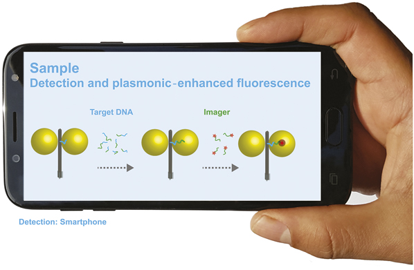
Owing to the sensitivity enhancement, signals of a few or even single molecules become visible. This brightness increment would render single molecules detectable with simple point-of-need devices. These platforms are typically designed to maximize compactness, lightness of weight, cost, and mobility and can be based on slightly modified smartphones (see Figure 3 ) Reference Wei, Acuna, Kim, Vietz, Tseng, Chae, Shir, Luo, Tinnefeld and Ozcan82 due to their worldwide availability and key features such as an integrated processor and a megapixel camera. Even larger enhancement factors can be attained by surface-enhanced Raman scattering-based detection, which also enables single-molecule detection. While a sheet of DNA between two nanoparticles can create an explicitly well-defined hotspot, it might become more challenging to still place capturing ligands between the NPs in a sub-10-nm gap due to the reduced volume available. Other transduction mechanisms could be explored when the binding event accompanies larger conformational changes. Changes in optical activity could be exploited to detect nucleic acid binding (Figure 2b, f). Reference Kuzyk, Schreiber, Zhang, Govorov, Liedl and Liu59–Reference Zhan, Dutta, Wang, Song, Dai, Zhao, Wang, Yin, Zhang, Ding and Ke61 Other possibilities include the conversion of a DNA walker capable of moving along a certain track within the origami structure such that each “step” can be exploited as a fluorescence amplification device. Reference Zhou, Duan and Liu60,Reference Wei, Acuna, Kim, Vietz, Tseng, Chae, Shir, Luo, Tinnefeld and Ozcan82,Reference Wang, Vietz, Schröder, Acuna, Lalkens and Tinnefeld83
Point-of-need devices for virus detection through DNA detection. (Left) If the target DNA is present, it hybridizes to the complementary strand protruding from the hotspot of the plasmonic cavity. At the second step, an imager strand modified with a fluorophore is added. The high fluorescence enhancement enabled by the plasmonic nanocavity can serve to detect single molecules with simple devices such as slightly modified smartphones. Reference Wei, Acuna, Kim, Vietz, Tseng, Chae, Shir, Luo, Tinnefeld and Ozcan82

Conclusions and perspective
For applications of DNA nanostructures in materials research, we see interesting challenges on the short and long length scales. On the short scale, the interface between chemistry and DNA nanotechnology could be improved, as DNA building blocks are more than one order of magnitude larger than the single-bond precision achieved in synthetic chemistry. On the long scale, self-assembly becomes less efficient due to the shallow hierarchy of bonds as well as due to the increased time of assembly associated with objects of increasing size.
Nevertheless, the capabilities of using DNA to preprogram the self-assembly of hybrid optical nanocomponents have already proven successful; however, a plethora of optical phenomena still remains to be explored using DNA nanotechnology. For example, nonlinear optics is one area where DNA can offer viable alternatives to conventional lithography. The resulting high confinement from DNA plasmonic nanocavities along with the placement of hybrid components to offer symmetry breaking can be used to produce high order harmonic generation. In combination with gain media, plasmonic lasers, so-called spasers, superradiant lasers, and other devices relying on cooperative effects can be pursued.
DNA-assembled 2D and 3D materials could help close the gap between the resolution limits of lithography and the requirements for materials that exhibit novel functionality in the optical frequency window. It remains to be seen if DNA nanotechnology can reach sufficient maturity to provide useful optoplasmonic devices, but for now, it certainly adds to the toolbox of current nanotechnologies.
Acknowledgments
This work was funded by European Research Council (ERC) through the ERC starting Grant No. 336440 for Optical Responses Controlled by DNA Assembly (ORCA), the BMBF (Point-of-Care-Diagnostik mit Einzelmolekül-Nachweis POCEMON, 13N14336), the Deutsche Forschungsgesellschaft (AC 279/2–1 and TI 329/9–1), and the Excellence Cluster Nanosystems Initiative Munich (NIM). We acknowledge support by the state ministry for research of Lower Saxony in the frame of the “Quantum- and Nanometrology” (QUANOMET) strategic research area. QUANOMET is part of the LUH-TUBS research alliance.

Mauricio Pilo-Pais is a postdoctoral researcher at Ludwig-Maximilians-Universität München, Germany. He obtained his PhD degree in physics from Duke University in 2014, and a double bachelor’s degree in physics and chemistry from the University of Florida in 2009. His current research focuses on developing and studying nanoscale elements for optical and plasmonic applications. Pilo-Pais can be reached by email at m.pilopais@lmu.de .

Guillermo Acuna leads the Bioapplications Group of the QUANOMET cluster, a research alliance between the Technische Universität Braunschweig and the Leibniz Universität Hannover, Germany. He obtained his PhD degree in Physics at the Ludwig-Maximilians-Universität München, Germany, in 2010. His current research includes the development of nanophotonic applications based on DNA nanotechnology. In 2016, he was a visiting researcher at the University of California, Los Angeles, where he worked on the development of plasmonic-based point-of-care diagnostic platforms. Acuna can be reached by email at g.acuna@tu-braunschweig.de.

Philip Tinnefeld has been a professor of physical chemistry at Ludwig-Maximilians-Universität München, Germany, since 2017. He received his PhD degree from the Universität Heidelberg, Germany, in 2002. He completed postdoctoral research at the University of California, Los Angeles, KU Leuven, Belgium, and Universität Bielefeld, Germany. He was associate professor of biophysics at Ludwig-Maximilians-Universität München, and then was appointed full professor of biophysical chemistry at TU Braunschweig in 2010. His current research focuses on combining optical single-molecule detection with DNA nanotechnology for self-assembled, functional devices. He has authored more than 140 publications and patents. He has been initiator and mentor of GATTAquant GmbH, the first company commercializing DNA origami applications. Tinnefeld can be reached by email at philip.tinnefeld@cup.uni-muenchen.de.

Tim Liedl has been a professor of experimental physics at the Ludwig-Maximilians-Universität München, Germany, since 2009. He obtained his PhD degree in physics in 2007 from the Ludwig-Maximilians-Universität München. From spring 2007 until summer 2009, he was a visiting researcher at the Dana-Farber Cancer Institute/Harvard Medical School, where he used the DNA-origami method to construct self-assembling two- and three-dimensional structures. His research interests focus on the interface of nanoscience, plasmonics, synthetic biology, and cell biology. Liedl can be reached by email at tim.liedl@physik.lmu.de.