I. INTRODUCTION
Near-field communication (NFC)-enabled smart-phones or other NFC readers used in buses, stores, and buildings make NFC technology ubiquitous to almost everywhere. Leveraging on-tag logic, larger memory, and more secure protocol, NFC has become a promising technology to replace Bar-code. Because of the low cost (a few cents), battery-free, and tap-to-go features, the NFC tag/card is widely used nowadays for access control, credit card payment, and logistic management [Reference Zhao, Smith and Sample1, Reference Zhao, Mahoney and Smith2].
Generally, the power consumed by single NFC tag in those applications comes from the magnetic signal transmitted by an NFC reader. Other than providing tiny data transfer for identification purposes, NFC can become a cost-efficient charging interface for portable devices. Commercially available NFC readers can transmit up to 750 mW continuous wireless power [Reference Strommer, Jurvansuu, Tuikka, Ylisaukko-oja, Rapakko and Vesterinen3] which can be used to energize some low-power smart devices. As an example, Battery-free passive NFC tag with enhanced computation and sensing features can be powered from commercially available NFC readers. These battery-free tags have many applications in healthcare management, patient monitoring [4–Reference Coskun, Ozdenizci and Ok6], and intelligent retail. Our previous work presents a software-defined NFC tag called NFC-wireless identification and sensing platform (WISP) [Reference Zhao, Smith and Sample1, Reference Dementyev7, Reference Zhao, Smith and Sample8]. Using a single high-Quality factor (Q) receiver antenna and a multi-stage rectifier to implement an efficient power harvester, the NFC-WISP hardware has a higher power harvesting efficiency comparing to existing NFC tags when tapped to an NFC reader. Besides, this platform leverages a general-purpose micro-controller, therefore, it is easily programmable for distinct applications with different on-board peripherals (such as temperature sensors, inertial measurement unit (IMU) sensors, nonvolatile FRAM memory, E-ink display, battery, etc). NFC-WISP can also be extended to more complex/custom applications through the extension headers and using a custom designed expansion shield. For example, the NFC-WISP can be used as a battery-free NFC temperature sensor by enabling the on-board thermometer, or it can be used as a semi-passive bi-stable E-ink display tag with the assistant of a re-chargeable battery.
A) Challenge
The amount of power received by an NFC tag from a reader is limited by its antenna specs and alignment, load impedance, range, and the transmit power, most of which fluctuate in different use cases. Besides, performing power demanding tasks (more than 1 mW) on the NFC tags or NFC-WISP is very challenging. For instance, updating an E-ink display on the NFC-WISP tag usually takes much more power (≈ 30 mW) than the continuously harvested power (max 6 mW if using a cell-phone reader [Reference Zhao, Smith and Sample1]). To overcome this challenge, the previous NFC-WISP design utilizes a small re-chargeable battery to buffer enough energy required for updating an E-ink. NFC-WISP then duty-cycles the display update operation at a rate such that the average consumed power by NFC-WISP is less or equal to average harvested power. But the use of battery limits the NFC-WISP's life-time and increases the maintenance overhead, size, and cost of the hardware.
Another challenge that commercially available NFC tags or NFC-WISPs [Reference Zhao, Smith and Sample1] suffer from is the limited placement freedom of the tag which constrains the usability of the NFC technology in practice (such as limited range and perfect antenna alignment requirements). For example, the antenna misalignment and changing in the tag's position and orientation, which may be varied with different users and use cases, can easily result in the failure of NFC communication. In addition, in our NFC-WISP applications, such as temperature logging and display, the different run-time processes or the use of distinct peripherals may result in the different load impedance of the NFC tag, thereby changing the power delivered to the load (PDL) or NFC communication performance. Disconnecting the load while delivering wireless power or doing communication can solve the problem of load variance, but it dramatically delays the application processing speed, which is already slow in passive tag scenarios.
Optimizing both PDL and communication performance is challenging because of a fundamental trade-off between wireless power efficiency and bandwidth of magnetic coils coupling. While a high coupling bandwidth is critical for ensuring robust and high-performance NFC communication, wireless power delivery efficiency boosts at lower coupling bandwidth. Traditionally, a single multi-turn loop coil is used in both NFC transmitter (reader or phone) and receiver (tag) to establish magnetic coupling for power delivery as well as in-band communication. Typically, high PDL achieved by using high-quality factor (Q) antenna, results in a narrow resonating bandwidth, therefore, limits the tag's reading distance and freedom of antenna alignment. The available space for increasing the Q of the transmitter (Tx) antenna in commercially available NFC readers is very limited and the modification cost is too expensive, especially in an NFC-enabled smart phone. For example, the intrinsic Q of the NFC antenna in the Nexus phone is around 15 [9]. Generally, the NFC ISO 14443 Type B protocol can maximize the transmitted power and communication speed due to the use of 10% amplitude-shift keying in its down-link as well as high communication bandwidth, which is critical for enabling power-hungry applications with large communication payload, such as updating display image on a display tag [Reference Zhao, Smith and Sample1, Reference Dementyev7]. Other protocol, such as ISO 14443 Type A and ISO 15693, either has limited transmitted power due to 100% modulation depth or slow communication speed [10, 11]. However, the ISO 14443 Type B tag requires a very low Q resonating system to provide a high bandwidth of minimal 1.906 MHz MHz to ensure successful up-link communication. This means, although the use of a high Q resonating design results in higher power delivery, it makes the communication of the NFC tag extremely vulnerable to the change of position, and is likely to result in the failure of data transfer. In practice, different users’ usage habits and scenarios, which can cause significant range and antenna alignment variation, severely limit the performance of the system.
B) Prior work
Traditional near-field wireless power delivery systems [Reference Waters, Fidelman, Raines and Smith12–Reference Hui, Zhong and Lee15], which are very similar to the NFC system but without communication features, use different numbers of coils (generally 2–4 coils in total) for different power transfer requirements. In a nutshell, the more coils used, the more parameter knobs are available for system optimization in terms of obtaining the highest power delivered to the load, optimal power delivery range and tolerance to the load variation. Our analysis [Reference Zhao, Mahoney and Smith2] shows that, if considering all the parasitic effects in practice, a 3-coil NFC system (with one high Q loop and one low Q load connected coil on the receiver and one coil on the transmitter) can deliver more power at smaller k while having limited communication performance (k is the magnetic coupling coefficient and negatively co-relative to the Transmitter(Tx)-to-Receiver(Rx) distance). On the other hand, a 2-coil system (single low Q receiver coil and one coil on the transmitter) has a wider resonant bandwidth and a better communication performance when k is very high but obviously lower power delivery efficiency.
C) Proposed idea
To overcome the above challenges, in this paper, we present a method, which can switch the NFC system between 2-coil and 3-coil configuration (including both Tx and Rx coils) to improve the wireless power delivery efficiency and obtain a reliable NFC communication. A programmable multi-coil receiver antenna controlled by a radio frequency switch is used for a new NFC-WISP 2.0 hardware. In addition, we show the challenges and trade-offs in the NFC wireless power delivery system, especially, when using an NFC-enabled phone as the power source. By finding the design sweet-spots, we ensure high power delivery as well as high bandwidth communication in different operation states or scenarios. Our contributions are listed and summarized below:
1. A theoretical analysis of the PDL given two distinct receiver antenna configurations in the NFC system is discussed.
2. A simulation work considering the variation of receiver load and fluctuation of reading distance or antenna alignment is presented.
3. The proposed method is implemented in a new version of the NFC-WISP 2.0, in which a configurable multi-coil receiver antenna is designed and discussed. It is illustrated how the 2-coil/3-coil switching method improves the system PDL, range, and communication robustness given varied system loads and states. The designed antenna is flexible so it can fit any curved surface and enable more applications.
4. The improved NFC-WISP hardware is shown to be used for battery-free but power-hungry applications with maximum operation duty-cycle and a cell-phone reader. As far as the author's knowledge, it is the first high-performance battery-free NFC tag that can be used to robustly update a 2.7″ E-ink display over the time period of 3 seconds and within upto 1.5 cm reading range in all usages and scenarios.
5. A smart label application using the designed NFC-WISP display tag and a customized Android application (App) in a smart-phone is demonstrated. The App allows the user to choose and edit an RGB photo from the phone, process it into a clear black and white sketch picture, and update the display of the NFC-WISP by tapping the phone onto the tag for only 3 seconds with a large 1.5 cm alignment tolerance.
II. OPTIMIZATION APPROACHES FOR THE NFC WIRELESS POWER SYSTEM
A) Optimization challenges and solutions
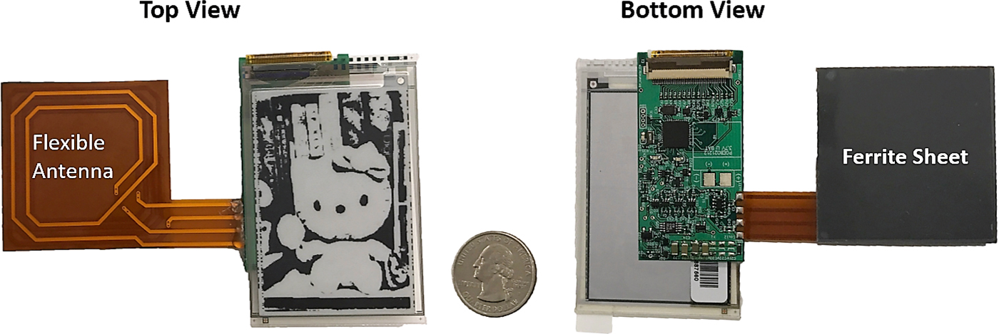
NFC reader can operate in three modes for different applications. When an NFC reader is in tag reader/writer mode, it can transmit about tens to hundreds of milliwatts of wireless signal into the air [Reference Zhao, Smith and Sample1, Reference Strommer, Jurvansuu, Tuikka, Ylisaukko-oja, Rapakko and Vesterinen3]. We design a passive/battery-free tag, NFC-WISP 2.0, to harvest the transmitted power from a magnetic coupled NFC reader. The obtained power is not only used for traditional NFC communication but also for any other enhanced features, such as computation, sensing, and display. The newly developed NFC-WISP tag is shown in Fig. 1, an NFC-enabled Galaxy Nexus phone is used as the reader for demonstration purpose in this paper. The previous NFC-WISP 1.0 hardware [Reference Zhao, Smith and Sample1] uses either a battery or a supper-capacitor to store harvested energy; whereas the new NFC-WISP 2.0 tag only utilizes a 500 µF ceramic capacitor to buffer the harvested energy. In general, to enable more power-hungry applications other than NFC communication running on the NFC tag, not only the NFC reader has to keep sending data (useful or dummy) in order to deliver sufficient power to the NFC-WISP tag, but also the NFC-WISP PDL performance has to be continuously high enough in all practical scenarios to prevent the system from brownouts. Demanding applications, whose power requirements exceed the instantaneous power harvested from the NFC reader, require duty-cycling and a large energy buffer (such as a super-capacitor or a battery) to store sufficient energy that can energize at least one operation cycle for a certain process. However, the use of the super-capacitors or batteries has many limitations: super-capacitors have higher leakage comparing to small ceramic capacitors and, therefore, limit the energy harvesting performance of the NFC-WISP; Besides, super-capacitors can provide smaller source current which avoids enabling applications with higher power consumption requirement; Batteries, especially Lithium-based batteries, have limited lifetime and its performance degrades over time. In addition, batteries and super-capacitors generally have a larger size and are more expensive comparing to a small ceramic capacitor, which is critical for space limited wearable or Internet-of-Things (IoT) applications [Reference Gubbi, Buyya, Marusic and Palaniswami16]. Increasing the PDL of the NFC-WISP system is a proper approach to solve the challenges caused by the use of a battery or a super-capacitor, besides, higher effective harvested power can further improve the operation speed, or in the other words, increase the duty-cycle. This plays a key role to achieve better usability and user experience. In the application section, we demonstrate how the new passive NFC-WISP 2.0 tag with improved PDL is able to update a display two times faster than what can be achieved by the battery-assisted NFC-WISP 1.0 hardware [Reference Zhao, Smith and Sample1].
Prototype of new battery-free NFC-WISP with flexible switchable receiver antenna and 2.7″ E-ink display.

Increasing the Quality Factor (Q) of the NFC reader (Tx) or the tag (Rx) antenna seems to be a method to improve PDL. However, the increase of the Q may not necessarily result in the maximum PDL given all reading ranges or receiver load impedance variations. In addition, high Q system design will limit the bandwidth of the system and dramatically degrade the NFC communication performance. When the NFC phone exchanges target data with the tag, especially during up-link (tag-to-reader communication), a high bandwidth of about 1.906 MHz is required because of the use of ISO 14443 protocol [17]. Due to the fundamental trade-off between bandwidth and Q, the NFC-WISP 2.0 tag has to adapt to the different requirement of Q and bandwidth in the different run-time period even in the same application. The system requires higher bandwidth during NFC communication process, thereby resulting in the lower system Q. In this particular case, the high bandwidth should be given the highest priority rather than wireless power performance; after the communication period, especially the up-link, has ended, the NFC reader or cell-phone can be configured to stream dummy data to power the tag. At this moment, NFC-WISP should maximize the Q to increase PDL efficiency.
As mentioned earlier, load impedance variations of the NFC-WISP during run-time is another parameter that can negatively impact the performance of NFC-WISP as well. Adaptive frequency or impedance tuning method is implemented in some of the wireless power transmitters [Reference Waters, Fidelman, Raines and Smith12, Reference Hui, Zhong and Lee15, Reference Waters, Sample and Smith18–Reference Park, Tak, Kim, Kim and Nam20] to compensate for the load variations of the NFC tags during run-time. However, the implementations of frequency or impedance tuning on commercially available NFC readers is challenging due to the following reasons; (a) the change of receiver load can occur within a short period (a few ms), the large controlling delay of the adaptive tuning methods makes the millisecond-level tuning very challenging or expensive. (b) frequency tuning violates both the NFC protocol and FCC regulations.
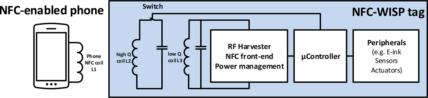
Therefore, we present a low-cost receiver antenna design in the new NFC-WISP 2.0 hardware to adapt to different system requirements at run-time and maintain high performance in different conditions. The receiver antenna of the NFC-WSIP 2.0 consists of two coils (Figs 1–3), one is high Q and is configured as a single frequency resonator with a tuning capacitor; the other is low Q and is connected to the receiver load. We use a switch controlled by the on-board microcontroller to control the wireless coupling between the high-Q resonator and the rest of the system. When the switch is off, the high Q resonator is open circuits and the NFC-WISP becomes a low Q receiver system; when the switch is on, the high Q coil gets attached and magnetically couples with the existing low Q receiver coil on the tag to create a totally different system in terms of Q and bandwidth. The detail system optimization analysis and approach are discussed in the following sections.
B) Circuit model and system analysis
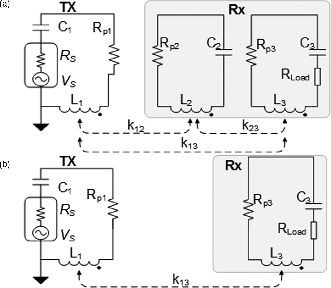
The circuit model of a 2 or 3-coil NFC wireless power system is presented in Figs 2 and 3. We simulate the system with three different Rx configurations given the same Tx and system load (V s, R s, C 1, R p1, L 1, R load remain constant): one is a 3-coil system and the other two are 2-coil systems. The overall Q of the wireless coupling link is dominated by the highest Q coil in the Rx. In a 3-coil system, the highest-Q Rx coil is L 2 and the 3rd coil connected to the load has a lower Q. The coupling coefficient k 12 in the 3-coil system and k 13 in the 2-coil system refer to the NFC reading distance and antenna alignment. In theory, the smaller the reading distance and the stronger the Tx-to-Rx coupling, the higher the k value. In the 3-coil system, k 23 is optimized for maximizing the average PDL over a 3 cm Tx-to-Rx range.
Architecture of passive NFC-WISP 2.0.

Block diagram of the NFC wireless power system: (a),(b) refer to 3-coil and 2-coil systems respectively. Tx is the NFC reader and Rx is the NFC tag. R pi and C i are the equivalent resistance and tuning capacitance of the coil i with inductance of L i. R s and R load are the source resistance of NFC reader and the equivalent resistance of the loaded hardware on the NFC tag. k ij is the coupling coefficient between coil i and coil j.

When using a smart-phone as an NFC reader, which comes with small Tx antenna dimensions and provides a low transmitting power, there are some limitations and assumptions as follows:
1. the max coupling coefficient k between the smart-phone reader and the NFC-WISP is estimated as 0.42 based on the dimension of the Tx antenna of a Nexus phone and NFC-WISP tag's antenna (which is 45 mm × 45 mm, 4 turns loop coil).
2. the ISO-14443 Type B NFC protocol requires at least a resonant bandwidth of above 1.906 MHz [17] due to its specific communication requirements, which is 5–20 times higher than typical wireless power systems [Reference Waters, Fidelman, Raines and Smith12, Reference Sample, Meyer and Smith19, Reference Kurs, Karalis, Mo_att, Joannopoulos, Fisher and Soljačić21, Reference Cannon, Hoburg, Stancil and Goldstein22].
3. In practice, the NFC tag reading range varies with humans” usage. Therefore, the design of the system should have a large tolerance to the change of relative antennas” position. In another word, the PDL and the NFC-WISP resonating bandwidth should be optimized given a large variation of k (overall system coupling coefficient variation due to antennas” misalignment).
4. Due to the load impedance variation of the NFC-WISP with peripherals and run-time software operating states, the design of the inductively coupled wireless power NFC system should be less sensitive to the change of load impedance. That means the optimization goal is to jointly optimize the PDL efficiency and the communication performance given the load variation as well.
From our previous paper [Reference Zhao, Mahoney and Smith2], we find that parasitic capacitance between each coil and the coupling between non-adjacent coils (L 1-to-L 3) result in significant resonant frequency shifting and PDL variation as k increases (the coupling becomes stronger). This prevents us from obtaining high-quality wireless power and communication performance in an NFC wireless power system. In general, the low Q 2-coil system can achieve an optimized PDL at larger k and the high Q 3-coil system can achieve an optimized PDL at smaller k. Briefly, given the same receiver load impedance, the 2-coil system can achieve better power transfer at a very close Tx-to-Rx range; In comparison, the 3-coil can lead to higher PDL at a larger range. However, the optimized PDL and its best range differ between 2-coil and 3-coil system and vary as the load impedance changes. In the following section, we explain how we can achieve PDL optimization with different k and receiver load impedances using our proposed switchable receiver antenna architecture design.
C) Load impedance variation
We simplify the reflected impedance from the load to the transmitter antenna in both 2-coil and 3-coil systems in equation (1). k 13 is ignored here to simplify the theoretical analysis. We will include the effect of k 13 and other parasitic effects discussed in [Reference Zhao, Mahoney and Smith2] in the following section. The  $Q_{2L_3}$ refers to the loaded Q of the entire two coils of the receiver in a 3-coil system, the
 $Q_{3L_2}$ refers to the loaded Q of the single receiver coil in a 2-coil system. In general, the
 $Q_{2L_3}$ is designed larger than
 $Q_{3L_2}$. Only when the RL is much smaller than the antenna parasitic resistance R p1, the
 $Q_{2L_3}$ will become larger than
 $Q_{3L_2}$. In most of the cases, by adding additional receiver coil, the reflected impedance seen by the transmitter becomes higher given the same receiver load impedance R L of the 2-coil system. That explains why, in the previous simulation, the 3-coil system has better wireless power efficiency in the far range (small k) while the 2-coil system has better performance in close range (large k). The maximized power delivery efficiency happens when the reflected load impedance conjugate matches the source impedance of the transmitter; as the range becomes closer, the reflected impedance becomes larger because of the stronger magnetic coupling. We call the coupling coefficient and the Tx-to-Rx distance where the n-coils system can match the transmitter source impedance as k mn, d mn. Since the reflected load impedance is an increasing function of k (k 13 in the 2-coil system, k 12 in 3-coil), the 3-coil system is likely to match the same source impedance at smaller k (longer distance). However, when the receiver load R L is too small (similar or smaller than R p1), Q L becomes extremely large and dominates the Q L3, therefore resulting in larger reflected impedance in a 2-coil system rather than a 3-coil system at smaller k. However, in this case, the best impedance matching happens at a very smaller k mn (normally large d mn), where, the absolute PDL becomes much smaller due to the long signal propagation distance. Compared to the case where the R L is medium and large, the PDL is much smaller when R L is too small over the same NFC reading range (03 cm). A medium R L can achieve impedance matching at larger k mn or smaller d mn, thus resulting in large PDL.
 $$\matrix{ {R_{ref{21}_3} = k_{12}^2 Q_1Z_1 \times \displaystyle{{Q_{2_3}} \over {1 + k_{23}^2 Q_{2_3}Q_{3L_3}}}\quad (3 - {\rm coil})} \hfill \cr {\quad \quad \quad = k_{12}^2 Q_1Z_1 \times Q_{2L_3}} \hfill \cr {Q_{2L_3} = \displaystyle{{Q_{2_3}} \over {1 + k_{23}^2 Q_{2_3}Q_{3L_3}}}\quad} \hfill \cr {Q_{3L_3} = \displaystyle{{Q_{3_3}Q_L} \over {Q_{3_3} + Q_L}}} \hfill \cr {R_{ref{31}_2} = k_{13}^2 Q_1Z_1 \times Q_{3L_2}\quad (2 - {\rm coil)}} \hfill \cr {Q_{3L_2} = \displaystyle{{Q_{3_2}Q_L} \over {Q_{3_2} + Q_L}}}\,. \hfill \cr} $$
In the most wireless power systems, the receiver antenna is designed not only to optimize the impedance matching to the transmitter but also to match the load impedance, which determines the optimal distance d opt where PDL is maximized. In a 2-coil system, there might be some impedance values for the transmitter and the receiver that cannot be matched given a particular load R L within the range d [Reference Kiani, Jow and Ghovanloo13]. In a 3-coil system, because of the use of one additional coil, we have more knobs to turn (k 23, Q 2) to optimize the impedance matching given any load R L within the same range d. The desired NFC reading range in most applications is 3 cm. Therefore, in this new revision of NFC-WISP design, we use an empirical k 23, which is optimized for obtaining better impedance matching over the target NFC-WISP reading range.
In practice, the load impedance R L may change between different processes in real-time. For example, in the cold start state, the NFC-WISP begins from zero power to power-on mode after harvesting enough energy. The load impedance R L of the NFC-WISP in this state is represented as  $R_{L_{coldStart}}$ (around 1 ohm in our measurement). However, after the NFC-WISP has been charged up and enters sleep mode, waiting for NFC reader interaction, the load impedance R L of the NFC-WISP becomes
 $R_{L_{sleep}}$, which is larger than
 $R_{L_{coldStart}}$ in our measurement. When the NFC-WISP is running power-hungry tasks, such as updating E-ink display (E-ink updating mode) or transmitting data to the NFC-enabled phone (Tx mode), it draws a significant amount of current (typically around 1–5mA) from the onboard energy storage element, the R L of the NFC-WISP then becomes
 $R_{L_{E - ink}}$ and
 $R_{L_{Tx}}$, which are larger than
 $R_{L_{sleep}}$. The variance of the load impedance is mainly introduced by the change of parasitics in the rectifier circuits and the changes of current drawn by the rest of the systems. (Please note that all the load impedance R L mentioned above is equivalent serial impedance measured from Vector Network Analyzer given 13.56 MHz transmitted frequency and the imaginary impedance is matched with tuning capacitor).
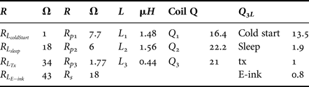
Therefore, the problem becomes: given a particular R L, how to choose the receiver antenna configuration (single receive coil or two) to optimize power delivery efficiency as well as keeping communication performance within the targeted NFC-WISP-to-Reader range (around 3 cm). Therefore, the designed antenna of NFC-WISP 2.0 can be switched to a low Q receive mode with a single receive coil (2-coil system) by opening the middle coilL 2, and can be switched to high Q receiver mode with two receive coils (3-coil system) by closing the middle coil loop L 2 (see Fig. 3). The architecture and prototype of the new NFC-WISP are shown in Figs 1 and 2. The measured parameters of the smart-phone reader and NFC-WISP are presented in Table 1.
Smart-phone and NFC-WISP measurements..

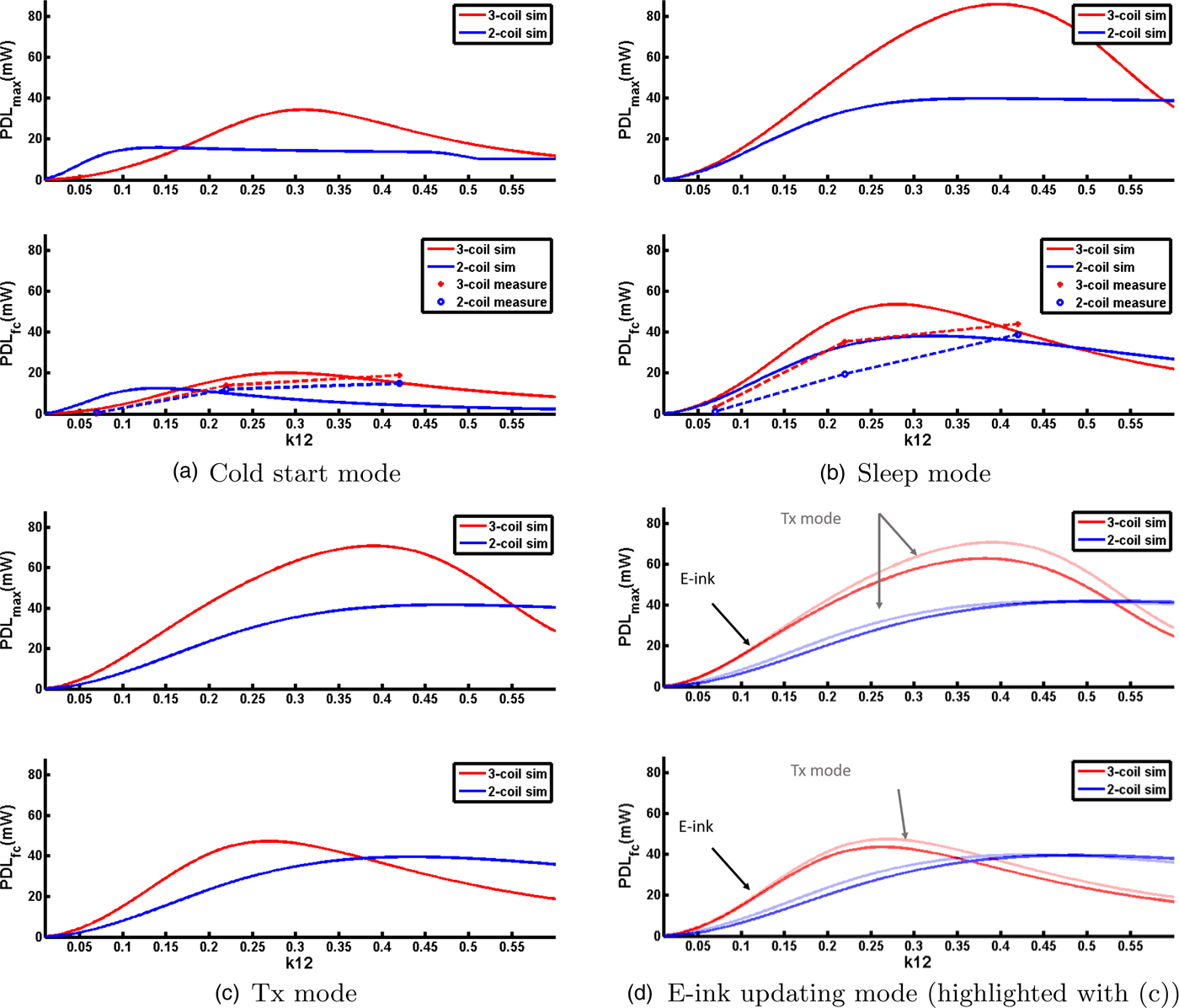
Considering all the parasitic effects mentioned in the previous chapter, the simulated PDL when the NFC-WISP is in different states is illustrated in Fig. 4. From the simulation results, we can find that when  $R_L = R_{L_{coldStart}}$, the PDL value becomes very small, because we use a parallel-connected tuning capacitor for tuning the NFC-WISP, which results in a small equivalent serial
 $R_{L_{coldStart}}$. A better matching network is suggested in the future work section to convert the load impedance to a better optimized R L in order to improve the overall PDL.
The simulated and measured PDL of NFC-WISP 2.0 (includes antenna parasitic effects and detuned L 2): PDL max is the maximum PDL at the resonant frequency(which may shift away from 13.56 MHz) when sweeping transmitted frequency. The PDL fc refers to the PDL when only transmitting a 13.56 MHz signal from an NFC reader. The simulated k 12 is between 0 and 0.6, however, in an NFC-WISP system, k 12 is around 0–0.42 in practice; the smart-phone case and complex hardware substrate lead to a reduction in the practical maximum for k 12 to <0.42.

III. SIMULATION AND MEASUREMENT RESULTS
From Fig. 4, we can conclude that when the R L is around 18–43 ohm, a 3-coil system (two receiver coils) has a better PDL if k 12 is around 0–0.45. In comparison, a 2-coil system will have a better PDL if k 12 is above 0.45 (given similar R s showed in Table 1). The measured reading range between NFC-WISP and phone (0−3 cm) results in a calculated k 12 of 0.42–0. This suggests that a 3-coil system is a better option when power performance is of higher priority than communication. But if a certain application requires the higher PDL while the achievable k 12 is around 0.42–0.65, then a 2-coil low Q system is suggested. Note that the increase of R L will change the threshold of k 12 where the PDL of a 3-coil system and a 2-coil system are equal. The simulation model used in Fig. 4 is based on Fig. 3, which neither include the nonlinear behavior of the rectifier and switch nor the interference of the smart-phone substrate. Besides, the noisy cell phone substrate will reduce the maximum k 12 below simulated 0.42 in practice. Therefore, the measurement result differs a bit from the simulation.
In general, the frequency of the max PDL will shift away from its original tuning frequency with an increase of k 12. That is because the parasitic capacitance and the cross-coupling effect become dominant as the range reduces. By detuning a 3-coil system to a lower frequency rather than to 13.56 MHz, we can shift the NFC-WISP working range. In our experiment, if we detune the high Q receiver coil L 2 to 12 MHz, we can shift the NFC-WISP up-link reading range from 2.8–3 cm to 0.8–1.65 cm. Typically, the PDL and communication performance, particularly the up-link, are very position-sensitive in a 3-coil system, mainly because of the larger frequency shift caused by the higher Q. An empirical suggestion is to detune the high Q coil L 2 of the NFC-WISP at 12 MHz given small k 12 in order to optimize the PDL within the entire range of 0.5–2cm. The achieved PDL here is sufficient for updating a 2.7″ display (more than 16mJ energy consumption). In conclusion, decreasing the tuning frequency of only high Q receiver coil can shift the operation range for power and communication in a 3-coil system. But a high Q 3-coil system, in general, is very sensitive to changes in relative antenna position.
(a) Cold start mode, (b) Sleep mode, (c) Tx mode, (d) E-ink updating mode (highlighted with (c)).
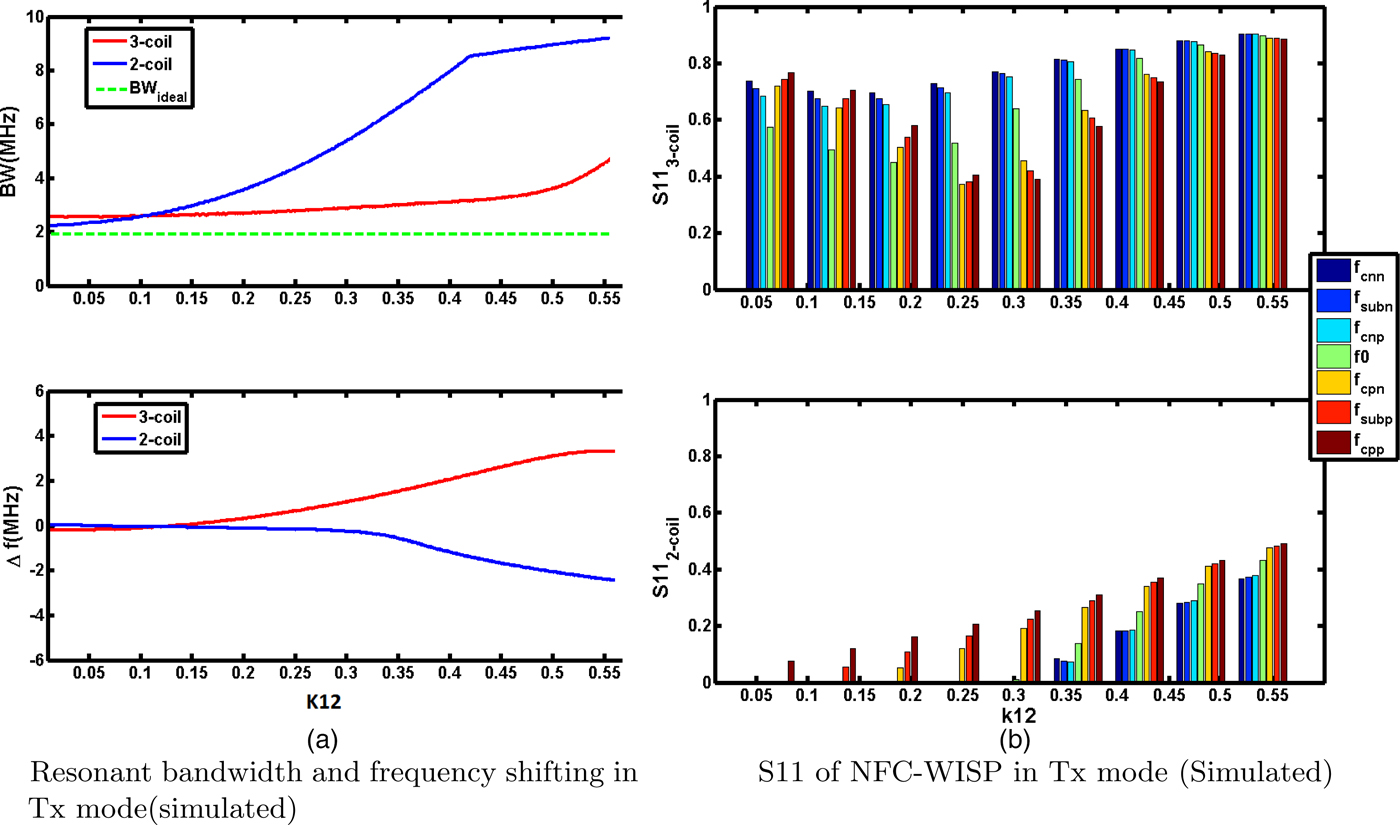
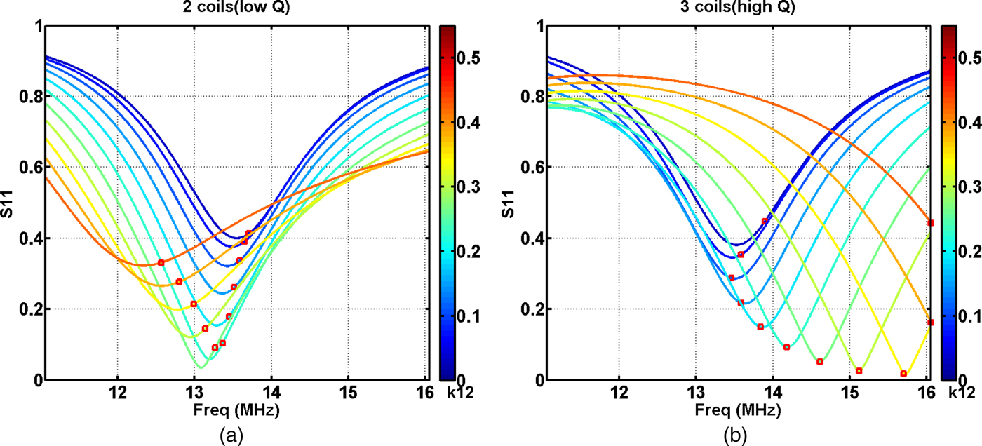
Typically, the NFC-WISP communication range is limited by its up-link. During the up-link (from NFC-WISP to Phone), the 3-coil system experiences a larger frequency shift compared to the 2-coil system, because the 2-coil system has lower Q. while Lower system Q reduces PDL, it ensures more robust communication because of its wide bandwidth as well as the smaller frequency shift. S 11 is a metric to determine the sensitivity of the up-link in an NFC communication system, lower S 11 value results in a higher SNR (signal to noise ratio) during load modulation. From Figs 5 and 6, we can also see that the 2-coil system normally has better S 11 even when considering the frequency shifting effect in Tx mode. The NFC 14443 Type B protocol requires at least 1.906 MHz up-link bandwidth [17]. In general, larger bandwidth can provide the capability of higher data rate and higher tolerance to the change of relative antenna position, so the 2-coil system suits for this purpose.
(a) is the bandwidth performance (includes antenna parasitics and detuned L 2: BW ideal refers to minimum bandwidth required by NFC protocol; the BW refers to the bandwidth of highest PDL (even when two resonant frequency appears) at resonant frequency, the resonant frequency normally shifts away from the NFC frequency as k 12 increases; Δf is the frequency offset of the highest resonant frequency to 13.56 MHz. In the NFC-WISP system, it is around 0–0.4. (b) is the S11 of NFC load modulation spectrum, f0 = 13.56MHz, f sub = 847.5KHz, f data = 105.9KHz, f subn = f0 − f sub, f subp = f0 + f sub, f cnn = f subn − f data, f cnp = f subn + f data, f cpn = f subp − f data, f cpp = f subp + f data. (k12 refers to the Tx-to-First Rx coil in all systems).

Simulated S11 of the 2-coil and the 3-coil systems in Tx mode (when  $R_L = R_{L_{Tx}}$) by sweeping transmitted frequency (x-axis); red square marks the resonant frequency where the PDL is maximum, the color of each plot refers to the simulation result with different k.

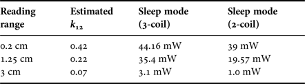
Different application requirements may have distinct priorities in regards to power, communication performance, reading range, and tolerance to the change of relative antenna position. The simulation and measurement results discussed in Figs 4 and 6 and Table 2, can help us choose the optimized configuration for each application based on our requirements.
PDL measurement comparison between the 3-coil and the 2-coil configurations in sleep mode.

For example, using a conventional NFC card or smart-phone case results in a minimum targeting reading distance of d. Then the application may require NFC tag reading and PDL optimization above the distance of d instead of 0 cm (when the antennas of the reader and the tag have a direct contract with each other). In this scenario, the 3-coil configuration should be chosen without changing the tag antenna design. Another example is that, if moderate and higher PDL and good communication are required over the entire range of 0–3 cm, we can switch to the 2-coil configuration in Tx mode and enable a 3-coil configuration in other modes to achieve both higher PDL and better communication. Please note that the optimization threshold of either k 12, range or other specs discussed in the paper will vary with different antenna specs in the different systems, but the overall optimization strategy will be similar as what we proposed with NFC-WISP 2.0 and NFC phone reader.
As a result, by implementing this proposed method in the second example, we can use the newly revised NFC-WISP to update a 2.7″ E-ink display within 3s with using a 500 µF capacitor as the charge reservoir and achieve a range of 0–1.5 cm while maintaining a robust communication. The old NFC-WISP hardware had to use a 10 mAh battery to provide sufficient power to update a 2.0″ E-ink display within 0–0.5 cm range and its updating speed is much slower than the NFC-WISP 2.0 hardware. The 2.7″ display consumes around 16 mJ energy, which is two times higher than the required energy for a 2.0″ display in general.
In conclusion, a low Q 2-coil system, which generates low PDL at far range, is less position sensitive and has good communication performance because of lower Q. But, in general, it is very sensitive to changes in load R L. The high Q 3-coil system can ensure higher PDL and communication at long range and is less sensitive to changes in load R L. However, it is very sensitive to changes in relative antenna position. Detuning the high Q coil in a 3-coil system can change the optimal reading position where the power performance can be maximized. By switching between low Q 2-coil (in Tx mode) and high Q 3-coil configurations (in another mode) in an application, we can obtain the overall optimization of both power and communication performance. The same analysis and approach can be used for other NFC tag optimizations that rely on dynamically adapting the Q value.
IV APPLICATION
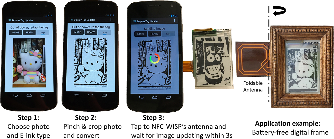
We develop an Android Application (APP) to show one possible usage of the new NFC-WISP 2.0 tag with switchable antenna: a battery-free digital frame (shown in Fig. 7). The APP also has the ability to select an image from any NFC-enabled Android phone, resize and crop the image, process the image to a 1-bit sketch photo, and transfer the image data (which is also transmitting wireless power) to the NFC-WISP tag. The wireless power obtained by the tag from the phone can support updating a 2.7″ or smaller E-ink display by Pervasive Displays [23]. The current APP supports 2.7″ and 2″ displays at the moment.
Updating display NFC-WISP with the designed app.

By clicking the “‘IMAGE” button in the application, the user can select any image stored on the phone. After selecting the image, it appears on the application and is ready for manipulation. The user can pinch and drag the image to zoom in/out and resize it to a target frame. After resizing the image to the desired size, the user can click the “‘READY” button to keep the frame after cropping and convert it into a 1-bit black-and-white sketch by applying a customized image filter. More image filters, such as Half-toning and Dithering filter, can be implemented in the future to create different image effects. The user can change the size of the image in the application to match the size of the E-ink display on the NFC-WISP tag by clicking toggle button at the top of the application. When the toggle button displays “‘large”, the current image size corresponds to a 2.7″ E-ink display. When the toggle button displays “‘small”, the current image size corresponds to a 2.0″ E-ink display. Then, the user can update the battery-free “Display tag” with the resulting sketch by tapping the phone onto the antenna of the tag. The APP can also send notification to the user about the state of the NFC-WISP in this application, such as “Tag detected”, “Sending image” and “‘Out of power, re-tap the tag”, to help the user understand the image transfer process and recover the failure by moving the phone away from the tag and re-tap it again. When the phone is in “Sending image state”, the screen on the phone will turn dark and a circular progress bar will show the image transfer progress in real-time to remind the user to stay tapped while image transfer is in progress.
The designed NFC-WISP display tag is able to tolerate around 1.5 cm phone-to-antenna position variation and delivers a maximum of 44 mW of power to the NFC-WISP tag with the proper receiver antenna configuration. In this application, the tag switches off the high Q antenna in between the rest of the antennas and turns the system into the 2-coil configuration in Tx mode (to optimize the communication), and switches on the middle antenna and enable the 3-coil configuration in other modes (to optimize the power). In our previous work [Reference Zhao, Smith and Sample1], we could only enable a smaller 2.0″ E-ink display updating (half the size of the 2.7″ one) on the NFC-WISP with the assistance of a thin-film battery at a shorter range (<0.5 cm). The battery-free feature of the newly developed NFC-WISP 2.0 display tag results in a lower hardware cost and application barrier. By putting the antenna on the side of the display instead of under the display (compared to the hardware in [Reference Zhao, Smith and Sample1]), the user can observe the change of display and align the cell-phone antenna with the NFC-WISP tag in a better way. Flexible antenna design allows the possibility to mount the tag on a curved surface or fold the antenna under the display when not used.
V. CONCLUSION
This paper presents an adaptive power and communication optimization method based on the simulation and analysis of an NFC wireless power and communication system in both 2-coil and 3-coil configurations. This system consists of a newly developed NFC-WISP hardware with switchable antennas and a commodity NFC-enabled smart-phone. Variations of load R L and coupling coefficient k between different NFC-WISP operating modes are simulated, and a switchable receiver coil design is proposed and shown to improve both power delivery and communication performance, which can be applied to future NFC wireless power applications. Finally, the use of the proposed method enables a new battery-free NFC-WISP application, in which we can use an NFC-enable smart-phone to update an E-ink display on the passive NFC-WISP tag. Our new design achieves large tolerance to the load variation and antenna alignment. Also, our new design enables operating at a longer distance (improved from 0.5 cm to 1.5 cm) while delivering two times more power than the previous version.
ACKNOWLEDGEMENTS
This work is funded by NSF Award CNS-1305072, Google Faculty Research Award, and Intel Science and Technology Center for Pervasive Computing.
 Yi Zhao received her Ph.D. degree in Electrical Engineering from University of Washington, Seattle in 2016.
 Huaye Li received a B.S. in Computer Engineering and Electrical Engineering from University of Washington, Seattle in 2017.
 Saman Naderiparizi A fifth-year Ph.D. student in the University of Washington Department of Electrical Engineering in Seattle, WA.
 Aaron Parks received his Ph.D. degree in Electrical Engineering from University of Washington in 2017.
 Joshua R. Smith received his Ph.D. in 1999 from Massachusetts Institute of Technology. Currently, he is an Associate Professor of Computer Science and Engineering, Electrical Engineering department of University of Washington, Seattle.