I. INTRODUCTION
Growth of wireless communications has spurred increasing possibility of using various application services with different frequency bands in the same mobile terminal. As part of serving the purpose, multi band antennas are desired for modern communication systems and 3G/4G wireless applications. Several techniques have been applied to design multiband antennas over the past years and these include stacked patches [Reference Zhou, Ch Chen and Volakis1, Reference Laheurte2], slot loading configurations [Reference Nguyen, Noghanian and Shafai3], CPW structures [Reference Chang, Shen and Lin4], monopole or planar antennas [Reference Lee, Lim and Yu5], and applying defective ground structures (DGS) [Reference Pie, Wang, Gao and Leng6–Reference Liu, Li and Sun8]. DGS are found to be simple and effective method in size reduction as well as excite additional resonance modes. Owing the interest towards achieving compact size, multiband, and impedance bandwidths, antennas such as aperture coupled stacked patch [Reference Pozar and Duffy9] and dual band circular polarization (CP) [Reference Yang and Wong10] are discussed. Enhanced bandwidth property is investigated using internal Planar Inverted F-type Antenna (PIFA) type multiband mobile handsets [Reference Zhang and Zhao11]. Stacked CP [Reference Wen, Chu and Shu12], slotted dual band CP [Reference Chen and Qing13], and DGS based monopole [Reference Liu, Wu and Dai14] antennas have been presented in recent literature for better 3-dB axial ratio bandwidths. Although, these antennas exhibit dual/tri-band characteristics, a limited bandwidth with large volume is exhibited at higher resonant modes. In [Reference Mok, Wong, Luk and Lee15, Reference Baek and Huang16], with the embedded U-shaped and L-shaped slots generates three distinct bands for WLAN/WiMAX applications, but poor radiation patterns in upper bands.
However the required −10 dB return loss bandwidth, 3-dB axial ratio (AR) bandwidth and gain need to be sufficiently improved.
In this paper, a novel tri-band planar antenna with DGS is proposed. The antenna consists of four T-shaped slits on all faces, asymmetric scaled slot placed at 45° center on radiating rectangular patch which satisfies the impedance characteristics as part of design criteria. Dual T-shaped slits on all sides of the patch provides the variation in bandwidth at higher resonant modes and gives dual band operation. Two orthogonal modes are generated due to the variation in the spacings (b ≠ c, a ≠ d) which produces CP at lower and middle resonant bands. The influence of the 45° slot cut produces an additional band for the structure in the form of better return loss and dual CP for two bands. By introducing proper asymmetry in the patch and slot, the degeneracy can be removed with one mode increasing with frequency while the orthogonal mode will be decreasing with frequency by same amount. The ground plane modified by loading it with circular shaped dumbbell makes the shift to a desired position of the resonant frequencies at all the three bands. The radius r and length Lg of the dumbbell can be adjusted to optimal dimensions in enhancing the impedance bandwidth of the antenna at lower and higher bands. This design process imposes a constraint on the gain of the patch antenna which in turn affects the miniaturization. By properly selecting and varying the dimensions of the proposed antenna, it can provide improved impedance bandwidths, frequency shift effect and working multiband. The antenna dimensions are optimized and simulated with the help of commercial EM software IE3D. Based on this study, the tri-band dual polarized antenna is constructed and measured. Good agreement exists for the measured and simulated results.
II. PROPOSED ANTENNA GEOMETRY DESIGN
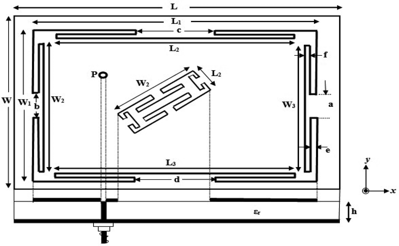
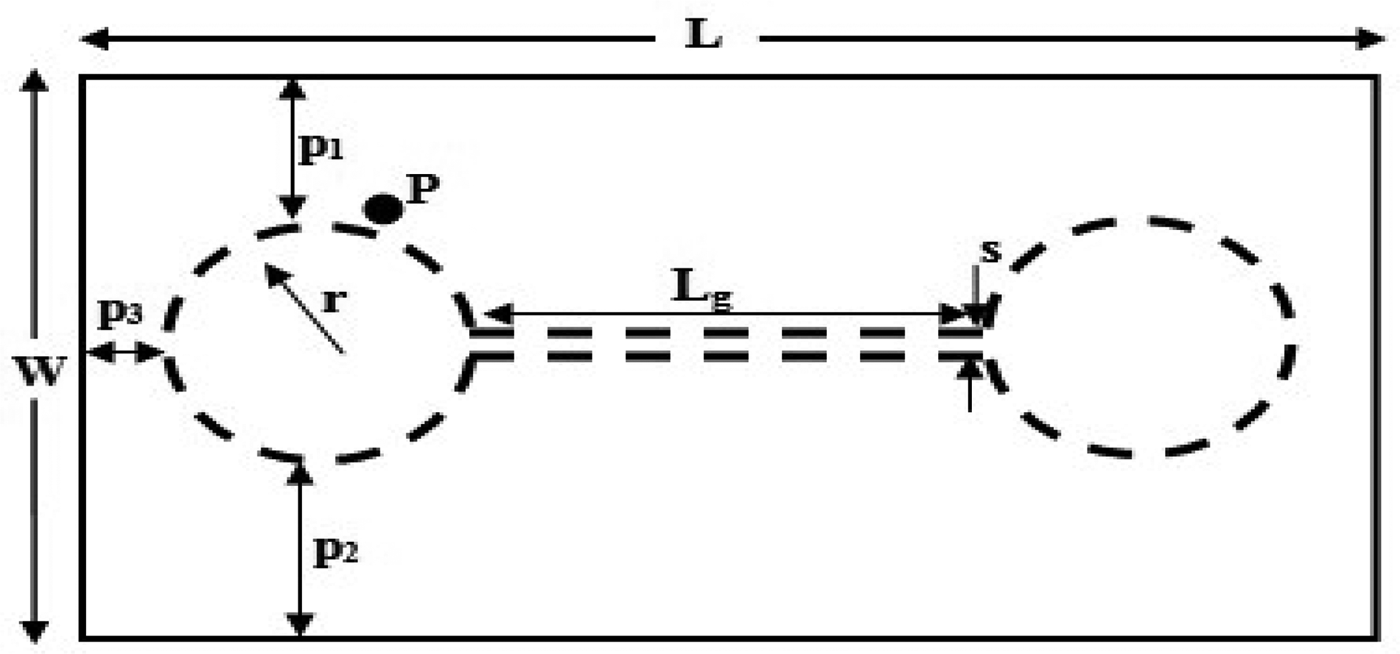
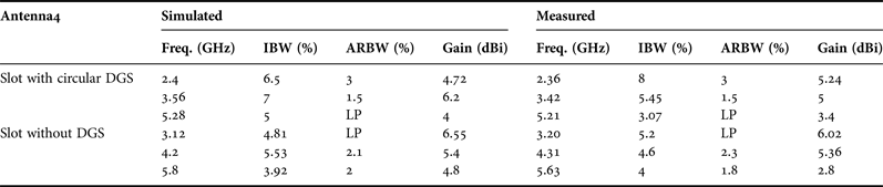
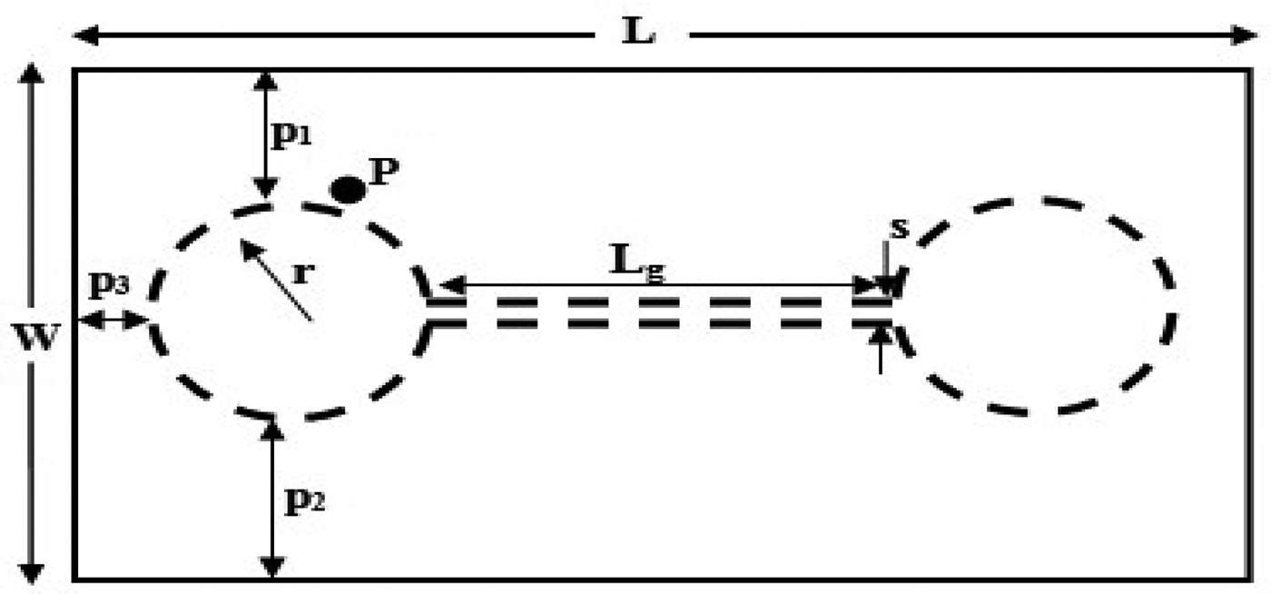
The configuration of the tri-band patch antenna under consideration is as shown in Fig. 1 and is patterned with 40 × 28 × 3.175 mm3 on Rogers RT/Duriod 5880 laminate with relative permittivity (ε r ) of 2.33 and loss tangent of 0.0012. Circular dumbbell shaped defect is printed behind the substrate as shown in Fig. 2. For comparison, the reference antenna (Antenna1) as shown in Fig. 3(a) is used and the return loss is plotted for iterative Antennas 1–4. The conventional rectangular patch antenna is chosen with dimensions L × W. T-shaped slits are introduced on all faces of the patch for dual frequency operation as shown in Fig. 3(a). A narrow rectangular slot is cut on the radiating patch as shown in Fig. 3(b) (Antenna2). The dimension of the narrow slot is adjusted by iterations to get a perfect dual band operation. Asymmetric slot with variation in spacing is cut as shown in Fig. 3(c) which enhances the bandwidth. A circular shaped dumbbell DGS with radius of “r” is chosen as the defect element on the ground plane. By controlling the shape of diagonal slot at the center of the radiating patch (Antenna3) in Fig. 3(c), the antenna resonates at multi bands. The circular dumbbell element is cut on the ground place in making the bands shifted as shown in Fig. 3(d) (Antenna4) to appropriate band positions used for wireless applications.
Top view of the proposed antenna geometry.

Bottom view of the proposed antenna geometry.
Design evolution of the proposed antennas 1–4.

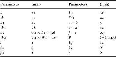
Table 1 gives the optimized dimensions of the radiating patch along with radius and length of DGS. In all the four iterative cases, the dimensions of the patch and slot size are unchanged. The achieved impedance bandwidth can be increased by introducing a defect element on the ground plane.
Dimensions of the optimized antenna design.
III. SIMULATION AND MEASUREMENTS
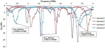
The spectrums and radiation patterns are simulated by using commercial Hyper Lynx IE3D software. The probe feed technique is chosen to have advantage of placing the feed at any desired location of the patch. Return loss is tuned by shifting the coaxial line feed point diagonally to accurate position “P” on the radiating patch. By adjusting the T-shaped slits, a dual band operation is obtained by Antenna1. The return loss spectrums of Antennas 1–4 are represented in Fig. 4. The frequency responses cover three bands of 2.26–2.45 GHz (bandwidth = 190 MHz, 8%), 3.41–3.6 GHz (190 MHz, 5.45%), 5.12–5.28 GHz (bandwidth = 160 MHz, 3.07%).
Simulated return loss for Antenna 1–4 evolved structures.

Through a number of simulations with iterative process, the position and dimensions of the slits and slots are optimized in producing tri-bands. Circular shaped dumbbell defect element allows us to vary the resonant frequency by changing the length without affecting the dimensions of the antenna. By introducing DGS, the current path is increased by which reduction in frequency occurs. DGS is helpful in the overall size reduction of the antenna structure.
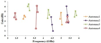
It is observed that the DGS geometry and optimized antenna parameter results in good impedance matching with high impedance bandwidth. The effect due to slits on the patch with circular DGS (Antenna1–Antenna4) on return loss (|S 11|) as a function of frequency is shown in Fig. 4. The variation of simulated gain with frequency is shown in Fig. 5.
Simulated gain response for Antenna 1–4 evolved structures.

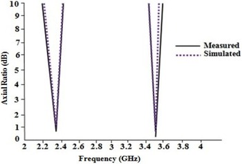
In the designed patch, the perturbation is in the form of diagonally placed asymmetric slot, which generates two modes with orthogonal linear polarizations (LP). It is seen that optimum dual CP is obtained by placing feed point diagonally (45° to the major axis) with frequencies equal to 2.4 and 3.56 GHz. The proposed antenna radiates a right hand CP wave within a 3 dB AR, caused by asymmetric slot at the CP center frequencies of 2.4 and 3.56 GHz, along with T-shaped slits with a right handed surface current. Diagonal feeding is required to allow both the modes to be excited with a single feed. Figure 6 illustrates the measured and simulated ARs plotted against frequency at mainly radiation direction for each band. The measured 3-dB AR bandwidths of lower and middle bands are about 40 MHz (2.38–2.42 GHz) and 11 MHz (3.51–3.521 GHz), respectively. The 3-dB AR bandwidth is within the 10-dB impedance bandwidth (over lapped), which is a desirable feature. It is observed that the Antenna4 gives 0.5 and 0.2 dB AR indicating good quality of CP (close to 0 dB) for the both 2.4 and 3.56 GHz bands, respectively.
Measured and simulated AR of Antenna4.

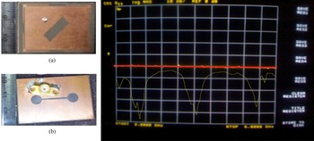
Pictorial representation of top view and bottom view fabricated antenna is shown in Figs 7(a) and 7(b), respectively. Figure 7(c) represents the measured response using the Agilent E5071C vector network analyzer.
Fabricated Antenna: (a) top view, (b) bottom view, and (c) response from network analyzer.

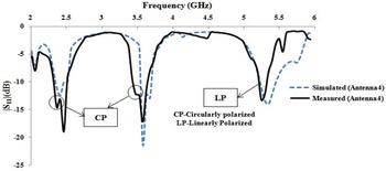
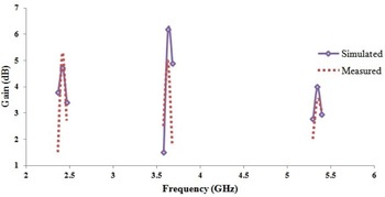
A simulated and measured return loss response against frequency for this triple frequency antenna is presented in Fig. 8. The measured and simulated frequency characteristics of peak gains for the proposed tri-band antenna are shown in Fig. 9.
Measured and simulated return loss of Antenna4 (with DGS).

Measured and simulated gain of Antenna4 (with DGS).

The measured gains of the proposed antenna are 5.24 dBi at 2.36 GHz, 5 dBi at 3.42 GHz, and 3.4 dBi at 5.21 GHz, respectively. As can be seen, stable gain variation across the three desired bands has been obtained. The gain of the proposed antenna within the operating bands satisfies the requirement of wireless communication terminals for WLAN and WiMAX operations.
Therefore compact size is achieved that affects the distribution of surface current density. However, the gain of the antenna is reduced for the antenna structure when DGS is applied to a conventional patch antenna.
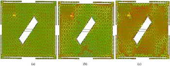
In order to study the excitation mechanism of the proposed antenna, the simulated surface current distributions of the whole antenna at the frequencies of 2.4, 3.56, and 5.28 GHz are given in the Fig. 10.
Average and vector current distributions at (a) 2.4 GHz, (b) 3.56 GHz, and (c) 5.28 GHz.

It can be clearly seen that the current distributions are different in the three bands. Most of the current flow is along the lower band excited at 2.4 GHz in Fig. 10(a), while surface current at 3.56 GHz is concentrated due to slot and latitude portion of DGS in Fig. 10(b). Current distributed for 5.28 GHz is mainly due to the symmetrical circular shapes for DGS on back side of patch as shown in Fig. 10(c).
The circular DGS slot placed on the ground plane excites at the resonant frequency expressed as [Reference Wen, Chu and Shu12],
 $$f_s = \displaystyle{c \over {2d\sqrt {\varepsilon ^{slot}}}}, $$
where d is length of the slot, ε slot is the effective dielectric constant.
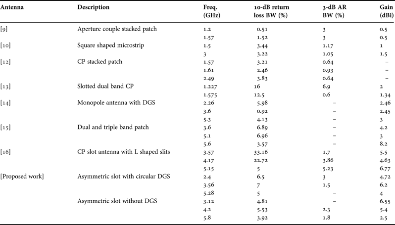
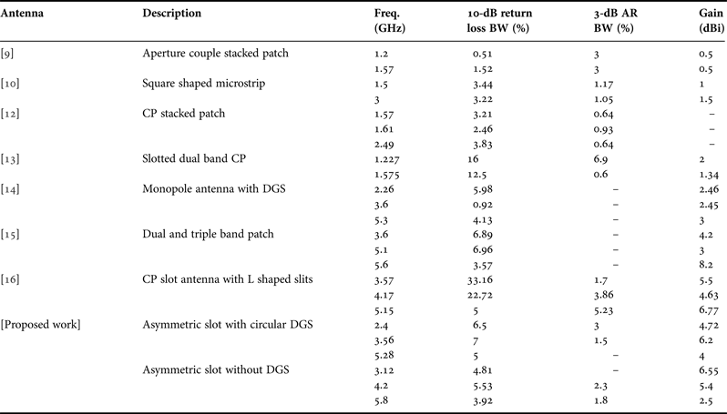
The radiator patch with circular dumbbell shaped DGS not only significantly improve the impedance matching conditions for the highest bands, but also can make the lowest and highest bands shift. Therefore, the DGS can be integrated onto the ground plane of such antenna in order to improve its radiation, besides not requiring additional circuits for implementation. Table 2 compares the results of proposed antenna with the existing probe feed dual- and tri-band planar antennas in the available literature. The presented antenna gives wider impedance bandwidth with a slight decay in the gain. The variation in the length of the DGS slot would seriously affect the third operation band impedance matching, whereas less change is seen for the first and second operation bands. The above analyzed results are in accordance with the proper selection of DGS structure and play vital role for designing the tri-band antenna. Miniaturization of the antenna is achieved by introducing DGS and drastic change in the reduction of the resonant frequencies.
Calculated bandwidth and gain parameters of the slot loaded antenna types.
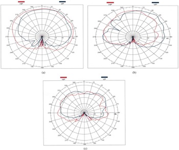
The far field radiation patterns are measured in anechoic chamber for the proposed antenna in the horizontal plane and vertical plane at resonant frequencies 2.4, 3.56, and 5.28 GHz, respectively are shown in Figs 11(a)–11(c). Because of the slot structure operated in 2.4 GHz band mainly, the asymmetrical lengths with in the slot affect the radiation patterns.
Measured radiation patterns at (a) 2.4 GHz, (b) 3.56 GHz, and (c) 5.28 GHz (represented in the x–y E-plane).

The proposed antenna is presented with useful CP and higher gain related to the previous works at these bands. The good performance of CP characteristic, suitable AR bandwidth, wider return loss bandwidth, available gain, and unidirectional radiation patterns are obtained. The antenna shows consistent radiation patterns at its different bands of operation despite having different current distributions at each frequency. This is accredited to the operation of the current distribution of the higher order resonant modes of the patch by strategic loading of different shapes of DGS. Furthermore, it is obvious that azimuthal variation of the polarization for dual linear or circular will take place.
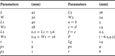
Table 3 shows the comparison of the proposed antenna with and without DGS element and also lists the simulated/measured parameters. The good performance of CP/LP characteristic, suitable AR bandwidth, wider return loss bandwidth, available gain, and better radiation patterns is obtained. As observed, the gain value is slightly compromised for the case of antenna with DGS element present. Increase in the thickness of the substrate also shows the impact in improvement of calculated gain at the frequencies of operation.
Summary of the simulated and measured parameters.
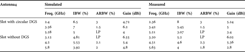
IBW, impedance bandwidth; ARBW, axial ratio bandwidth; LP, linear polarization.
VI. CONCLUSIONS
Tri-band patch antenna with DGS is designed, simulated, and tested for wireless applications. Antenna structure with and without defective ground plane are presented and compared. The DGS technique makes it possible to reduce the resonant frequencies of TM mn modes of Antenna4 by 24, 19 and 8% respectively, compared with Antenna2 occupying the same area. Measured and simulated AR bandwidths are in good agreement and gives better CP for dual bands. This paper was focused on better CP with reasonable AR bandwidth besides reducing the size of the antenna without compromising the gain. The measured and simulated resonant frequencies of the modes and respective impedance bandwidths of the patch antennas were observed to be in excellent agreement. The gain values at the operating frequencies of novel structure were also investigated. Similar and symmetric radiation patterns at all bands of operation were obtained. The study elucidates the trade-off between the compactness via DGS with gain. The proposed antenna is applicable for wireless communication systems with enhanced bandwidth especially for WLAN/WiMAX bands.
ACKNOWLEDGEMENTS
The authors would like to acknowledge Prof. N.V.S.N. Sarma, Professor in Department ECE, NIT Warangal for his immense support during the fabrication and measurements of the developed tri-band antenna.
 B. Rama Sanjeeva Reddy received his Bachelor's degree from University college, Bangalore, India and Master's degree in Microwaves from Government College of Engineering, Pune, India. He is presently working in the field of antenna arrays at National Institute of Technology, Warangal, India.
 D. Vakula obtained her Bachelor's degree in Electronics and Communication Engineering from Nagarjuna University, AP, India and Master's degree from Birla Institute of Technology, Mesra India, with Microwave specialization in the years 1992 and 1994, respectively. She obtained Ph.D. on Fault diagnostics of Antenna Arrays from National Institute of Technology, Warangal, India in the year 2010. She is working as Assistant Professor at National Institute of Technology, Warangal, India since 2006. She has published 20 papers in International Conferences and Journals. Her areas of interest include phased array antennas, ultrawide band antennas, multiband antennas, fault diagnostics, and neural network.