


I. INTRODUCTION
The continuously growing interest in mobile devices requires low-power wireless transceivers achieving Gbps data rates. The unlicensed 57–66 GHz spectrum around the oxygen absorption peak presents a great opportunity for high-speed short-range wireless communication and higher millimeter (mm)-wave frequencies in E-band are already being targeted for high-speed communication at longer ranges due to better transmission. Scaling in CMOS technology provides higher f t and f max in each technology node [1], thus enabling a viable solution for mm-wave-integrated circuits at lower cost and smaller system size.
Since breakdown is limiting the supply voltage in CMOS technology, producing high-power levels requires power combining [Reference Jiashu and Niknejad2]. However, the passive structures needed for such schemes introduce additional loss at mm-wave frequencies through resistive and substrate loss and require relatively high DC power. Although 60 and 70 GHz-band CMOS power amplifiers (PAs) with P sat over 10 dBm have been reported in the resent years [Reference Kurita and Kondoh3–Reference Asadi and Yagoub6], very few of them show wideband large-signal performance. Such performance is required if multiband communication applications are pursued to increase the total aggregate data rates through the use of multiple bands in the V- and E-bands. A common CMOS PA at mm-wave frequencies in addition to the output matching for maximum power requires the inter-stage matching. Wideband techniques such as negative feedback or resistive matching cannot be implemented because of limited gain of the transistor at these frequencies. In [Reference Kurita and Kondoh3], flat gain is achieved by shaping the cut-off frequencies of transmission-line-based matching networks is presented. Transmission lines shows very reliable mm-wave models with well-defined current return path and good agreement between simulated and measured data, but are more suited for single-ended design, consume significant silicon area, and draw relatively high DC power due to losses. In [Reference Suzuki, Kawano, Sato, Hirose and Joshin4], a short stub transmission line topology was used to reduce the losses and Q-factor of the network was kept low to achieve wideband matching. Transformer-coupled topologies [Reference Jiashu and Niknejad2, Reference Chan, Long, Spirito and Pekarik5] show compact and simple layout especially for differential topologies, provide a relatively wideband matching capability, as shown below in Section III. Lumped-element-based designs [Reference Asadi and Yagoub6] that use LC matching facilitates small layouts but typically show more narrow band performance because of the resonance used in the matching network and high transformation ratio resulting in high network Q-factor.
In this work, we propose the use of transformer-coupled differential cascade CMOS stages to enable wideband large-signal performance of PAs at E-band. The proposed topology is shown in Section II. Section III describes the inter-stage matching; Section IV shows the simulated and measured results, and conclusions are drawn in Section V.
II. PA CIRCUIT DESIGN
The PA is a differential three-stage transformer coupled design in 90 nm 1P9M low-leakage CMOS process. The schematic is shown in Fig. 1.
Circuit schematics.

Each stage has a differential cascode configuration. The cascode topology shows better isolation, improved bandwidth and gain compared to common source (CS), but need higher supply voltage to allow sufficient headroom. The increased supply allows larger voltage swing but reduces the achievable efficiency. The differential topology was chosen to lower the even-order harmonics, reject common-mode noise and provide ideally 3 dB more output power compared to a single-ended device of the same size. Utilization of on-chip transformers allows compact RF matching, stabilization and easy DC biasing through the virtual ground points. Input and output baluns are used to allow single-ended measurement with Ground-signal-ground (GSG) probes and a two-port Vector network analyzer (VNA). A summary table of the designed transformers simulated performance at 70 GHz is shown in Table 1.
Transformers simulated performance at 70 GHz.

The output power delivered by transistor in class A is limited by P out < V DDI Q where V DD is the supply voltage and I Q is the transistor bias current. Thus, in order to increase the output power under the process limitation of maximum allowed V DD, the transistor drive current capability has to be increased through its size, because of V gs and minimum channel length L are fixed by the design in order to maximize f t or f max of the transistor [Reference Dickson7]. This can be done by increasing the number of fingers and keeping the finger width constant or keeping the same number of fingers and increasing the finger width. A larger finger width results in higher gate finger resistance. Higher gate resistance hardly affects the f t, but reduces f max and hence the maximum stable gain. Maximizing the f max and G max provides the upper limit in the finger width, thus further increasing the total gate width requires increasing the number of the fingers. It can be shown theoretically that f max is independent of the number of the fingers [Reference Doan, Emami, Niknejad and Brodersen8]. The number of fingers was limited in our case by RF NMOS model (to 32 fingers) while further increasing demand connecting number of transistors in parallel, which increases parasitic inter-connect losses leading to lower f max and MSG.
Load pull simulation combined with output stability and power gain circles was performed to the output stage. For the output stage four transistors M3 (32 * 2 µm/90 nm) were chosen to satisfy the maximum gain and output power trade off, achieving output power of 14 dBm and power gain of 8 dB at 60 GHz. The bias point was chosen near the peak f t current density by setting the PA at class A. The achievable P sat varies over the frequency, with values of 14, 13.5, and 12.8 dBm for 60, 70, and 80 GHz, respectively. Figure 2 shows a load-pull simulation of constant power contours for the lowest saturated output power minus 1 dB, i.e. 11.8 dBm, delivered by output stage at 60, 70, and 80 GHz. The circles drawn show the desired load impedance range needed for wideband large signal PA performance if 1 dB flatness in P sat is desired.
Constant output power contours, Z Load and power gain of the output stage (inset).

Additional stages are needed to achieve more power gain. The size of each stage transistors is chosen as half the size of the following stage in order to ensure that the output stage enters compression first, the second stage after it and the first stage saturates the last.
III. INTER-STAGE MATCHING
An integrated transformer can be modeled by [Reference Niknejad9] as an ideal transformer with turn ratio N, as shown in Fig. 3, where L 1 is the primary coil inductance and L 2 the secondary, and k is the coupling factor defined as 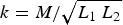 $k=M/\sqrt {L_1\, L_2 }$, where M is the mutual inductance.
Integrated transformer model and inter-stage conjugate matching process.

Figure 3 illustrates the operation of the transformer XF2 that matches the second and first stages from 60 to 73 GHz. S 44 represents the impedance looking into the transformer loaded by the second-stage input (S 11) that needs to conjugate match the output impedance of the first stage, represented by S 22. There are several challenges in the design of an on-chip transformer. The insertion loss of the transformer can be minimized by increasing the coupling coefficient and maximizing the Q of the two coupled inductors. The self-resonance frequency (SRF) needs to be high enough to keep the impedance transformation less frequency dependent.
Initial transformer parameters were calculated based on the analytic model by three steps, first assuming k = 1 as shown in Fig. 3. The turn ratio N was calculated as square root of ratio of real impedance parts represented by S 11 and S 22. The real part of the impedance represented by S 11 is smaller relatively to that of S 22 because it represents input resistance looking into the gate of the CS transistor. An ideal transformer with the turn ratio N brings S 11 from points 1 to 2 moving on the constant Q path, thus increasing the impedance by N Reference Jiashu and Niknejad2. In the second step, L 1 is calculated to match the reactive part of the impedance. This ideal inductance move the S 44 from points 2 to 3 close to the desired S 22*. Finally, L 2 is calculated as L 1/(N Reference Jiashu and Niknejad2). Co represents the inter-winding capacitance of about 6fF that responsible for the SRF of the transformer at 110 GHz. Due to ideal transformer that is used in the model the Q-factor of the matching network remain constant and low, compared to any ideal LC matching network that will increase the Q because the series reactance will not move on constant Q path. Multistage network can reduce the network Q (thus achieving better matching bandwidth) but introduce additional losses and consume more area.
With initial parameters of L 1 and L 2, the transformer was implemented in two top metals 9 and 8 with 3.25 and 0.5 µm copper thickness, respectively. The lower thickness of the bottom metal was compensated by a larger trace width. The larger inductance in metal 9 was implemented using two coplanar loops in series. Electromagnetic simulation using MomentumTM was performed to maximize the coupling factor k, which is about 0.7. As shown in Fig. 3, if S 44 is close to S 22*, with a calculated reflection coefficient of better than −8 dB from 60 to 73 GHz, and better than −4.5 dB from 73 to 80 GHz.
The output transformer loaded by 50 Ω needs to provide the large signal Z Load to the output stage, whereas the input transformer matches the input stage to 50 Ω at small signal. Figure 2 also shows Z Load at 60, 70, and 80 GHz, which are the impedances looking into the transformer XF4 loaded by 50 Ω taking into account the GSG pad capacitance at these frequencies. It can be seen that using transformer coupling a wideband large signal matching is achieved. It can be seen in the inset of Fig. 2, that selecting Z Load to achieve flat and high output power drops the power gain (G p) of the output stage when the frequency increases, which has an impact on the gain flatness as shown below.
IV. SIMULATED AND MEASURED RESULTS
The chip micrograph of the PA is shown in Fig. 4. The PA occupies the area of 0.25 mm2 including the bond pads. All the measurements were performed using on-chip probing. The simulated and measured S-parameters of the amplifier are shown in Fig. 5. Measured linear gain has a peak of 18 dB at 63 GHz and a 3 dB bandwidth of 8 GHz (from 60 to 68 GHz). S 12 is better than −35 dB across the frequency range because of cascode topology used and not shown for clarity. The amplifier is unconditionally stable over the entire measured frequency range with stability factor greater than unity.
PA micrograph.

Measured and simulated small-signal performance.

Large-signal performance of the PA was measured by a V-band power detector and a signal generator aided by an active multiplier to cover the entire band. The detector and multiplier output power were calibrated at the probe tip using the on-chip probing setup over the frequency and power level. Figure 6 shows the output power, P O1dB and peak power-added efficiency (PAE) of the PA from 55 to 80 GHz. At the supply voltage V DD of 2.2 V, the measured 1 dB compressed output power has a peak of 7.2 dBm at 71 GHz and 1 dB flatness is achieved across 17 GHz from 62 to 79 GHz. Maximum saturated output power has a peak of 11.9 dBm at 73 GHz with 1 dB flatness of 15 GHz from 62 to 77 GHz. Figure 7 shows the output power, gain, and PAE of the PA at 67 GHz as function of input power, demonstrating a peak PAE of 4.6% when the output power is 11 dBm and the gain is 7.5 dB.
Measured large-signal performance.

Measured PA output power, gain, and PAE at 67 GHz.

V. DISCUSSION AND CONCLUSION
Implementation of cascode topology in this design allows a large V DD voltage, compared with other in Table 2, providing relatively large output power at the cost of efficiency. Utilization of on-chip transformers allows compact design and broadband small signal as well as large signal matching. In this work, the largest 1 dB flatness frequency range in both P 1dB (17 GHz) and P sat (15 GHz) was achieved, demonstrating a broadband large signal operation at V- or E-band. The focus of this work was to achieve a significant P sat (more than 10 dBm) over a wide-frequency range to support multiband communication applications at V- or E-band. Matching for power over a wide-frequency range comes at the cost of the small signal gain 3 dB bandwidth and 1 dB flatness, which is less important if the total bandwidth is used by several carrier frequencies. The gain flatness could be improved by sacrificing reflection loss at the lower frequencies of the band, again at the expense of efficiency and the peak gain. In addition, saturating the output stage at frequencies with less gain require proper sizing of the driver stage, at the cost of degraded efficiency.
Comparison with state-of-the-art CMOS PAs at V- and E-bands.

*Includes bond pads.
†Estimated from figures.
‡Pout 3 dB flatness.
 Igor Gertman received a B.Sc. in Electrical Engineering from Tel Aviv University in 2008, where he is now working toward the M.Sc. degree in Electrical Engineering. His main research interests are design and optimization of high-power microwave power amplifiers in CMOS technology.
 Eran Socher earned a B.A. in physics (Summa Cum Laude), and B.Sc. (Summa Cum Laude), M.Sc., and Ph.D. degrees in electrical engineering, all from the Technion — Israel Institute of Technology. From 2006 to 2008 he was a visiting researcher at the High Speed Electronics Laboratory and a visiting assistant professor in the Department of Electrical Engineering at the University of California at Los Angeles (UCLA). Since October 2008, he is a Senior Lecturer at the School of Electrical Engineering of Tel Aviv University, where he founded and heads the High Frequency Integrated Circuits Laboratory. He has co-authored over 50 journals and conference papers, and he is the recipient of several teaching and research awards and scholarships, including the Rector Prize for Teaching and HPCA Best Paper Award. His research interests are currently focused on RF and mm-wave CMOS circuit design for high data rate communication, sensing, and imaging.



