I. INTRODUCTION
Photovoltaic devices based on organic–inorganic hybrid perovskites have been attracting more and more attention lately especially as their power conversion efficiency (PCE) has recently surpassed 20%. Reference Zhou, Chen, Li, Luo, Song, Duan, Hong, You, Liu and Yang1–Reference Burschka, Pellet, Moon, Humphry-Baker, Gao, Nazeeruddin and Grätzel3 In addition to their high performance, their potential low cost, earth abundant elements and solution processability have also been sources of excitement. Reference Schlipf, Docampo, Schaffer, Körstgens, Bießmann, Hanusch, Giesbrecht, Bernstorff, Bein and Müller-Buschbaum4–Reference Guo, McCleese, Kolodziej, Samia, Zhao and Burda7 The organic–inorganic hybrid perovskite compounds based on metal halides are represented as AMX3 perovskite structure, where A is an organic cation, most often methylammonium (CH3NH3 +) or formamidinium (HC(NH2)2 +), M is a metal cation (typically Sn2+ or Pb2+) and X is a monovalent anion (typically a halide ion Cl−, Br−, or I−). Reference Hao, Stoumpos, Chang and Kanatzidis5,Reference Munir, Sheikh, Abdelsamie, Hu, Yu, Zhao, Kim, Tall, Li, Smilgies and Amassian8
Several deposition methods have been developed for perovskite film preparation such as: one-step solution deposition, Reference Lee, Teuscher, Miyasaka, Murakami and Snaith2,Reference Jeon, Noh, Kim, Yang, Ryu and Seok9,Reference Rong, Tang, Zhao, Zhong, Venkatesan, Graham, Patton, Jing, Guloy and Yao10 two-step (sequential) solution deposition, Reference Burschka, Pellet, Moon, Humphry-Baker, Gao, Nazeeruddin and Grätzel3,Reference Schlipf, Docampo, Schaffer, Körstgens, Bießmann, Hanusch, Giesbrecht, Bernstorff, Bein and Müller-Buschbaum4,Reference Yang, Noh, Jeon, Kim, Ryu, Seo and Seok11–Reference Zheng, Wang, Yang, Liu and Sun13 and one-step or two-step vapor deposition. Reference Hao, Stoumpos, Liu, Chang and Kanatzidis14,Reference Liang, Mitzi and Prikas15 The two-step sequential deposition method is one of the earliest and most widely used protocols to be developed for the synthesis of hybrid perovskite thin films. It was first developed to overcome the challenges associated to the formation of pin-hole free films using the single step solution process. Reference Burschka, Pellet, Moon, Humphry-Baker, Gao, Nazeeruddin and Grätzel3,Reference Shen, Yu, Cai, Peng, Ma, Su, Xiao and Zou16,Reference Zhang, Mao, He, Zhang, Zhu, Xie, Wong, Grätzel and Choy17 In the two-step solution process, the PbI2 powder is first dissolved in dimethylformamide (DMF) then spin-cast on the substrate prior to its annealing and exposure to a solution containing methylammonium iodide (MAI) or formamidinium iodide (FAI) dissolved in iso-propyl alcohol (IPA). Reference Schlipf, Docampo, Schaffer, Körstgens, Bießmann, Hanusch, Giesbrecht, Bernstorff, Bein and Müller-Buschbaum4,Reference Yang, Noh, Jeon, Kim, Ryu, Seo and Seok11 During conversion of PbI2 into MAPbI3, the perovskite phase is believed to form through a conversion reaction at the PbI2–MAI interface. This process has been shown to be impacted by the MAI concentration in solution, the annealing temperature and by the microstructure and morphology of the PbI2 film. Reference Zheng, Wang, Yang, Liu and Sun13,Reference Zhou, Yang, Vasiliev, Garces, Zhao, Wang, Pang, Zhu and Padture18 Wu et al. affirm that the state of the PbI2 film greatly affect the microstructure of the polycrystalline perovskite film. Reference Wu, Li, Liu, Zheng, Xue, Liu and Gao19 Hence, the ability to tune the morphology of PbI2 can help address one of the important challenges faced during the two step deposition process, namely the incomplete conversion of PbI2 films in inaccessible parts of the sample which can lead to recombination losses and instability of the perovskite phase and related optoelectronic devices. Reference Cao, Wang, Yu, Zhou, Lu, Zhao and Wong20 Several approaches have been developed to tune the morphology of PbI2 films with the aim of preparing high quality, stable polycrystalline perovskite films and to fabricate highly efficient solar cells, including by modifying solution concentration and growth time, Reference Liu, Hu, Wu, Chen, Zhao, Liu, Wang, Lu, Jia, Russell, Zhu and Gong21 by use of additives Reference Zhou, Yang, Vasiliev, Garces, Zhao, Wang, Pang, Zhu and Padture18 or by emerging methods such as the solvent–solvent extraction method. Reference Zheng, Wang, Yang, Liu and Sun13 Importantly, several studies have pointed to porous PbI2 films as being easier to convert into the perovskite phase, yielding higher PCE in comparison to conversion from more dense and compact films. Reference Zhou, Yang, Vasiliev, Garces, Zhao, Wang, Pang, Zhu and Padture18,Reference Cao, Wang, Yu, Zhou, Lu, Zhao and Wong20 The existence of pores in PbI2 films is expected to facilitate mass transport, easier access by MAI to the entire PbI2 volume, and because of their ability to accommodate the volume expansion associated to formation of the MAPbI3 phase. This has been linked to formation of films with fewer pin holes and reduced residual PbI2 content. Reference Zhou, Yang, Vasiliev, Garces, Zhao, Wang, Pang, Zhu and Padture18
Yet, despite the apparent simplicity and undeniable success of the two-step procedure in yielding highly efficient solar cell devices, it is not understood in great detail, especially as the metal halide can form intermediate solvate phases, which might have either positive or negative implications on subsequent conversion to the targeted lead halide perovskite phase. Reference Schlipf, Docampo, Schaffer, Körstgens, Bießmann, Hanusch, Giesbrecht, Bernstorff, Bein and Müller-Buschbaum4,Reference Yang, Noh, Jeon, Kim, Ryu, Seo and Seok11 The single-step hybrid perovskite formation process using DMF was recently investigated in situ and shown to proceed via the formation of disordered and/or ordered precursor solvate phases which strongly dictate the microstructure and morphology of the converted hybrid perovskite film. Reference Lee, Teuscher, Miyasaka, Murakami and Snaith2,Reference Munir, Sheikh, Abdelsamie, Hu, Yu, Zhao, Kim, Tall, Li, Smilgies and Amassian8,Reference Rong, Tang, Zhao, Zhong, Venkatesan, Graham, Patton, Jing, Guloy and Yao10 A similar behavior can be plausibly expected during solution processing of the lead halide PbI2 from a DMF solution. Indeed, this has been reported to form PbI2–solvent complexes in different solvent systems, such as dimethyl sulfoxide (DMSO). Reference Yang, Noh, Jeon, Kim, Ryu, Seo and Seok11,Reference Li, Fan, Li, Mai and Wang22 For instance, Hao et al. have reported that an intermediate phase can form during the solution-based two-step process which are clearly absent when vacuum co-deposition is used instead. Reference Hao, Stoumpos, Liu, Chang and Kanatzidis14 Yet, these phases have been observed ex situ and their formation history during solution-processing is not fully or sufficiently understood. We take the view that achieving a deeper understanding of intermediate phase formation during metal halide solution processing is very important toward subsequent conversion of the hybrid perovskite phase, its morphology and microstructure, and to fabricate high performance solar cells reliably and reproducibly. Reference Shen, Yu, Cai, Peng, Ma, Su, Xiao and Zou16,Reference Grancini, Marras, Prato, Giannini, Quarti, De Angelis, De Bastiani, Eperon, Snaith, Manna and Petrozza23
In this work, we investigate the formation of the metal halide PbI2 from a DMF solution. To do so, we have performed in situ time-resolved grazing incidence wide-angle X-ray scattering (GIWAXS) measurements during the spin coating process to observe its solution-to-solid phase transformation. Reference Müller-Buschbaum24,Reference Hexemer and Müller-Buschbaum25 These measurements are complemented with ex situ X-ray diffraction, atomic force microscopy (AFM), and scanning electron microscopy (SEM). Our study demonstrates that PbI2 deposition proceeds via a sol–gel process whereby a disordered precursor solvate (<20 s) gives rise to the sequential formation of two ordered solvates, the first emerging during solution drying from ∼20 to 60 s and the second one forming subsequently until the PbI2 phase begins to form ∼5–6 min later. The air-drying of films from these precursor phases leads to the formation of continuous yet substantially more porous and rough PbI2 films than when the as-cast film is placed immediately on a hotplate for drying and annealing at 100 °C. The air-dried films achieve the same crystal structure and approximate crystallite size as the latter. The observation that intermediate solvates form with limited lifetime of tens to hundreds of seconds can be leveraged to impact conversion of the hybrid perovskite film if the process and formulation are adjusted accordingly. Reference Zheng, Wang, Yang, Liu and Sun13,Reference Liu, Hu, Wu, Chen, Zhao, Liu, Wang, Lu, Jia, Russell, Zhu and Gong21,Reference Chou, Khan, Niazi, Yan, Li, Payne, Anthony, Smilgies and Amassian26 Our findings suggest that the intermediate solvates and air-dried PbI2 should be considered as alternative starting materials for conversion into hybrid perovskites rather than compact PbI2. We anticipate this study to generate new conversion schemes which might increase the quality and optoelectronic properties of perovskite films and perhaps further improve the reproducibility of the two-step manufacturing processes.
II. EXPERIMENTAL PROCEDURE
A. Substrate preparation
Glass substrates were cleaned successively in detergent, deionized water, acetone and isopropanol in an ultrasonic bath for 15 min each. Subsequently, the substrates were treated with UV-Ozone for 10 min.
B. Thin film fabrication—lead iodide solution preparation and deposition
To prepare the PbI2 precursor solution, 461 mg of as-purchased lead (II) iodide powder (PbI2, Alfa Aesar, Ward Hill, Massachusetts) were mixed in 1 mL of anhydrous dimethylformamide (DMF, Sigma-Aldrich, St. Louis, Missouri). The solution was stirred overnight at 80 °C. All precursor materials were used directly without purification. The PbI2–DMF precursor solution of 40 μL was spin coated at 1000 rpm for 5 s and 2000 rpm for different spin coating times onto the glass substrates. The substrates were either transferred to a hotplate preheated to 100 °C, and the thermal treatment lasted for 10 min or were left to dry in air for 30 min. All the synthesis and deposition of PbI2 layer was carried out in N2 filled glove box with humidity level less than 1 ppm unless otherwise stated.
C. Characterization techniques
1. Grazing incidence wide angle X-ray scattering (GIWAXS)
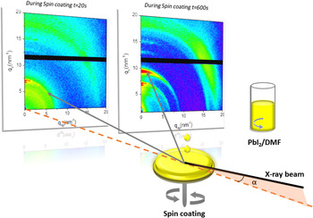
Grazing incidence wide angle X-ray scattering (GIWAXS) measurements were performed at the D1 beam line at the Cornell High Energy Synchrotron Source (CHESS). A 0.5 mm × 0.1 mm monochromated X-ray beam (double-bounce multilayer monochromator) with a wave length of 1.16 Å (10.6 keV) was used. GIWAXS data was collected with a Pilatus 200k pixel array detector (Dectris, Baden-Dättwil, Switzerland; 100 frames per second) placed at a distance of 92 mm from the sample. An incidence angle of 0.25° (above the estimated critical angle of 0.22°) with respect to the substrate plane was used and an exposure time of 0.2 s was used to balance between time resolution and signal quality. In situ time-resolved GIWAXS measurements were performed during spin coating using a custom-built and computer-controlled spin coater equipped with a Kapton splash guard, as previously described Reference Munir, Sheikh, Abdelsamie, Hu, Yu, Zhao, Kim, Tall, Li, Smilgies and Amassian8,Reference Chou, Khan, Niazi, Yan, Li, Payne, Anthony, Smilgies and Amassian26 (see Fig. 1). As the hutch needs to be closed prior to starting in situ experiments, we estimate a 1 min delay between solution casting and start of spin-coating and simultaneous in situ GIWAXS measurements. In situ experiments were conducted in ambient atmosphere with relative humidity ∼20–25%.
Schematic representation of the in situ GIWAXS measurement setup combined with a spin-coater.

2. Atomic force microscopy
The surface topography and root mean squared (RMS) roughness were measured in semi-contact mode on 10 × 10 µm2 areas using a Dimension Icon atomic force microscope (AFM; Bruker Nano Surfaces Division, Santa Barbara, California). The measurements were performed with a scanning speed of 1 Hz in ambient air, at room temperature, with relative humidity in the 40–60% range.
3. Scanning electron microscopy (SEM)
Scanning electron microscopy (SEM) images were acquired using a Zeis Auriga microscope (Carl Zeiss NTS GmbH, Oberkochen, Germany) with in-lens detector using a 5 kV accelerating voltage and a beam aperture of 30 μm.
III. RESULTS AND DISCUSSION
A. In situ time-resolved grazing incidence wide angle X-ray scattering (GIWAXS) measurements
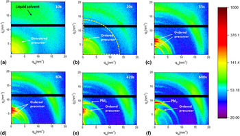
We investigate the PbI2 film formation from solution processing by performing in situ time-resolved grazing incidence wide angle X-ray scattering (GIWAXS) measurements during spin coating, as shown in Fig. 1. Reference Munir, Sheikh, Abdelsamie, Hu, Yu, Zhao, Kim, Tall, Li, Smilgies and Amassian8,Reference Chou, Khan, Niazi, Yan, Li, Payne, Anthony, Smilgies and Amassian26 Two-dimensional GIWAXS snapshots taken at different periods of spin-coating of PbI2 for a total duration of 10 min are shown in Fig. 2. In the early stages of spin coating (∼10 s), the scattering features are dominated by two scattering halos: one at high q values is associated with the liquid solvent, Reference Perez, Chou, Love, van der Poll, Smilgies, Nguyen, Kramer, Amassian and Bazan27 while a second at low q values is associated to the disordered sol–gel precursor, which we name P0. Reference Munir, Sheikh, Abdelsamie, Hu, Yu, Zhao, Kim, Tall, Li, Smilgies and Amassian8 As the solvent continues to dry (∼20 s), we begin to see sharp scattering features q z ∼7 nm−1 indicating formation of the ordered precursor phase. Continuing GIWAXS measurements reveal a dynamically evolving set of precursor scattering features (55, 80, 420, and 600 s). The precursor scattering features lose intensity at later times (420 and 600 s) and the PbI2 (100) diffraction ring makes an appearance and increases in intensity, indicating the complexes transform into the pure PbI2 phase.
In situ GIWAXS snapshots collected during spin-coating of a PbI2 solution in DMF at (a) 10 s, (b) 20 s, (c) 55 s, (d) 80 s, (e) 420 s, and (f) 600 s. Scattering features associated with the disordered and ordered precursor solvates are identified, as is the (100) diffraction of PbI2. The circular dashed lines in (b) delineate the integration area for generating Fig. 3.

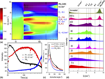
The time-evolution of the scattering features—after integration for each time slice—is plotted in a 2D intensity map with respect to time (abscissa; 7 < t < 600 s; logarithmic) and q (ordinate; 2 < q < 10 nm−1) in Fig. 3(a). The length of the scattering vector q is determined by the following equation:
 $q = \sqrt {q_z^2 + q_{xy}^2}$
, where:
 ${q_z} = {{4\pi \sin {\alpha _{\rm{f}}}} \over \lambda }$
,
 ${q_{xy}} = {{4\pi \sin {\theta _{\rm{f}}}} \over \lambda }$
, and λ is the wave length.
Reference Perez, Chou, Love, van der Poll, Smilgies, Nguyen, Kramer, Amassian and Bazan27
The time-evolution reveals an abrupt transition at ∼21 s from a broad scattering halo at low q range (q < 7 nm−1), associated to the wet sol–gel precursor state (P0), to sharp diffraction features, attributed to formation of a transient ordered precursor solvate phase,
Reference Munir, Sheikh, Abdelsamie, Hu, Yu, Zhao, Kim, Tall, Li, Smilgies and Amassian8
which we name P1. The diffraction features associated with P1 are observed at q = 4.2, 6.4, 6.7, and 8.1 nm−1 and are very short-lived, lasting tens of seconds. As the features associated to P1 disappear almost simultaneously, we see the emergence of new diffraction features, which we attribute to a second transient precursor phase, P2. The diffraction features associated to P2 are observed at q = 6, 6.7, and 7.0 nm−1 and are more long-lived, lasting more than 200 s before the eventual appearance of the (100) diffraction feature of PbI2 seen at 9.1 nm−1. It is important to note here that diffraction features which we have attributed to P1 and P2 could also be coming from multiple solvate phases, but this is rather unlikely as the scattering features appear and disappear at nearly identical times. We see this as indicating that P1 and P2 are two different solvate polymorphs with P1 the less stable of the two. In Fig. 3(b), we plot the time-evolution of the integrated intensity of the diffraction features of P1 (4.2 nm−1), P2 (6.1 nm−1), and PbI2 (9.1 nm−1), while in Fig. 3(c) we plot pole figures associated to P1 (∼30 s), P2 (∼80 s), and PbI2 (∼600 s). Intensity plots corresponding to different time slices are shown in Fig. 3(d) to highlight the complex evolution of the as-cast thin film microstructure. The pole figures reveal all phases have comparable texture and mosaicity, with the crystalline phases formed at different spin-coating times predominantly oriented in the out-of-plane direction. An interesting observation is the apparent degradation and broadening of some of the sharp diffraction peaks formed between 30 and 80 s at later times when PbI2 formation is detected. This may indicate that the crystalline solvates may degrade first into a more disordered phase before the crystalline PbI2 phase forms.
(a) Time-evolution of 2D GIWAXS intensity map of the spin-coating process of PbI2 in DMF showing P1 and P2 ordered precursor solvate phases and PbI2 (100). (b) Time-evolution of the diffraction intensity associated to P1 (4.2 nm−1), P2 (6.1 nm−1) and PbI2 (9.1 nm−1) phases. (c) Pole figures of the P1, P2 and PbI2 phases as measured in situ. (d) Intensity plots at designated time slices (5, 15, 20, 30, 55, 80, 420, and 600 s) during spin-coating of PbI2 in DMF and for a thermally annealed sample.

Our in situ diagnostics reveal the intermediate solvates of PbI2 and DMF formed during spin-coating tend to be unstable. Others have reported that an equilibrium complex of PbI2·DMF can be formed into a monoclinic single crystal with P21/n space group (a = 4.54 Å, b = 18.27 Å, c = 11.59 Å, β = 92.69°). Reference Wakamiya, Endo, Sasamori, Tokitoh, Ogomi, Hayase and Murata12 Wakamiya et al. have shown that this equilibrium solvate contains one DMF molecule coordinated with Pb forming one-dimensional structures of PbI2⋅DMF along the a axis. Reference Wakamiya, Endo, Sasamori, Tokitoh, Ogomi, Hayase and Murata12 In thin films, the PbI2 interlayer spacing has been shown to expand along the c axis to retain DMF solvent molecules, forming a PbI2·DMF complex. Reference Hao, Stoumpos, Liu, Chang and Kanatzidis14 Zheng et al. have attributed the pale yellow color observed during the initial seconds of spin coating to a PbI2·DMF complex. Reference Zheng, Wang, Yang, Liu and Sun13 This phase is represented by two strong peaks at 9.02° corresponding to q = 6.4 nm−1 and 9.56° (∼9.46° in Ref. Reference Shen, Yu, Cai, Peng, Ma, Su, Xiao and Zou16 corresponding to q = 6.7 nm−1). These peaks correspond to the (011) and (020) planes of PbI2·DMF, which appear to match a small subset of diffraction features seen in Figs. 3(a) and 3(c). However, it is difficult to attribute these peaks with confidence to the diffraction features observed in the spin-cast precursor solvate, which is probably a non-equilibrium precursor, just like in the case of single-step spin-coating of PbI2 and MAI in DMF. Reference Munir, Sheikh, Abdelsamie, Hu, Yu, Zhao, Kim, Tall, Li, Smilgies and Amassian8
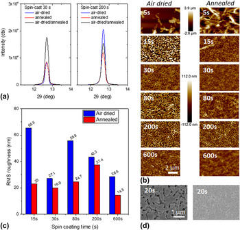
The intermediate solvates of PbI2·DMF observed during spin coating ultimately lead to the spontaneous formation of the PbI2 phase in ambient air at room temperature without requiring thermal annealing, suggesting they are metastable. The in situ investigation of spin coating lasted only 10 min, during which time the solvate scattering features decreased in intensity but did not disappear, while PbI2 (100) diffraction intensity increased. We have prepared additional samples by spin-coating them for a short duration of 30 s and left them to dry in ambient air at room temperature for 30 min while others were placed immediately on a hot plate and annealed at 100 °C for 10 min. In Fig. 4(a), we plot the XRD data for PbI2 final films spin-cast for 30 s after they were left to dry in air or annealed. The (100) diffraction peak is located at the same angle (12.68°) and the peak intensity is comparable, Reference Hao, Stoumpos, Liu, Chang and Kanatzidis14 indicating the PbI2 microstructure is fully developed irrespective of the drying method. Annealing to 100 °C therefore appears to induce faster drying rather than enhancing the degree of crystallinity of the film. In fact, additional annealing of the air dried samples does not show substantive differences in diffraction peak intensity, indicating that the crystalline structure of PbI2 is well developed upon drying in air and that annealing mainly serves to accelerate the conversion process from the P1 or P2 phases of PbI2·DMF to pure PbI2. Atomic force microscopy (AFM) was used to investigate the surface morphology of the PbI2 films prepared using the different approaches, as shown in Fig. 4(b). The AFM images reveal a poorly formed film for extremely short spin coating durations of ∼5 s as the film is still composed of liquid solvent and wet precursor sol–gel [Figs. 2 and 3]. The wet film is therefore likely to be subject to excessive dewetting which results in the formation of large and tall isolated crystals observed by AFM. When the film is spun for a longer duration (>15 s), the resulting films are substantially more continuous, irrespective of the drying method used, as revealed by comparing AFM images in Fig. 4(b). The film formed after 15 s spin coating consists of a wet sol–gel film that is mostly free of liquid solvent.
(a) X-ray diffraction spectra of PbI2 films prepared by spin coating for 30 and 200 s, followed by drying in air at room temperature for 30 min or annealing at 100 °C for 10 min or air-dried and annealed. (b) AFM topographic images of PbI2 films spin cast for 5, 15, 30, 80, 200 and 600 s and subsequently air dried or annealed. (c) RMS surface roughness of the films featured in (b). (d) SEM images of PbI2 films spin cast for 20 s and subsequently air dried or annealed.

Closer inspection of the continuous films by AFM [Fig. 4(b)] and SEM [Fig. 4(d)] reveals important differences between the surface morphologies of air-dried and annealed samples. The films show uniform polygon-shaped grains and scattered voids among adjacent grains in both cases. Reference Hao, Stoumpos, Liu, Chang and Kanatzidis14 However, the surface of the air-dried films exhibits a slightly irregular and open morphology consistent with AFM images. This may be due to the slow evaporation of the DMF solvent while drying in air. We further investigate the impact of the drying method on films spin cast and arrested during either the P1 or P2 phase and left to dry in air for 30 min (different durations, namely 15, 30, 80, 200, and 600 s) and post-processed according to the two drying methods. AFM images of these films [Fig. 4(b)] and the root mean squared (RMS) roughness values summarized in Fig. 4(c) reveal that air-dried PbI2 films are substantially rougher than annealed ones, showing greater roughness by a factor of 2–3 for 15, 80, and 600 s. Smaller differences in surface roughness on the order of ∼15–30% are seen for 30 and 200 s. The roughness of air-dried films decreases for longer spin coating durations (200 and 600 s), while the roughness of annealed samples appears to remain consistently lower than that of air-dried samples for all spin coating durations.
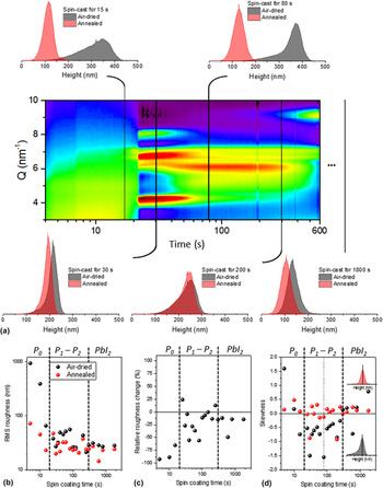
The variations in the roughness of air-dried samples previously spin-cast for different durations merits further investigation as the duration of spin-coating determines the state of the PbI2·DMF film from which immediate annealing or slow air drying is performed. To do so, we have plotted in Fig. 5(a) the distributions of surface height obtained from AFM measurements of key samples along with the corresponding state of the film as revealed from in situ GIWAXS measurements. The distributions featured in the top row correspond to the cases showing the largest variations, whereas the ones at the bottom represent the cases where the drying method does not appear to influence the morphology to the same extent. As all distributions have been set to zero, the height position of the peak and its tail reflect how deeply and frequently the AFM tip is able to probe below the surface of the film. Consequently, the broad and skewed distributions shown for air-dried films in the top row of Fig. 5(a) reveal the film to have an open structure with pores and grain boundaries reaching deep into the film. In case of annealed samples, we observe consistently narrower and more symmetric distributions of surface height, indicative of more compact films with lower surface roughness. The films featured in the bottom row show a different behavior. Interestingly, the samples spun for around 30 s and air dried yield a much smoother film than the others, an observation we have verified by repeating the experiment. This suggests that the morphology of PbI2 films is compact and insensitive to drying method when the as-cast films are in the highly ordered P1 solvate phase.
(a) Distributions of surface height obtained from AFM analysis of samples spin-cast for durations of 15, 30, 80, 200, and 600 s, along with the time-evolution of GIWAXS data showing the structural evolution of the disordered and ordered PbI2⋅DMF complexes as well as the PbI2 phase formation. Distributions at 15, 80, and 600 s show very large differences, whereas distributions at 30 and 200 s are more similar. (b) RMS roughness of dozens of samples prepared by spin coating anywhere from 5 s to 1800 s. (c) Relative change of RMS roughness between air-dried and annealed PbI2 samples. (d) Skewness of the height distributions obtained from AFM analysis of all samples.

To further quantify and refine these observations we have fabricated dozens of PbI2 films by spin coating them for different durations from 5 s to 1800 s and leaving them to dry in air for 30 min or immediately annealing them at 100 °C. The results of AFM analyses are summarized in Figs. 5(b)–5(d), respectively, in terms of RMS roughness, relative change of roughness between air-dried and annealed samples, and skewness of the distributions of surface height. Figures 5(b) and 5(c) confirm that spin coating samples for 10 s or less and air-drying results in significantly greater roughness than if the same samples are immediately annealed. The same data plot reveals significant difference in roughness when longer spin-coating times are implemented to dry the films from the P1 and P2 states. We observe convergence in roughness for spin coating times exceeding 5 min, when the PbI2 phase has clearly begun to form. The skewness of the height distributions of the same set of samples is shown in Fig. 5(d) to be consistently near zero and very slightly positive for almost all annealed samples and samples air dried after extended spin-coating (>5 min). However, we find that all samples air dried from the P1 and P2 states are negatively skewed and significantly so, indicating that these samples are characterized by a more open structure accessible well below the surface by the AFM tip. The AFM analysis reveals that PbI2 film morphology appears to be sensitive to the state in which the as-cast film is prior to drying in air or at elevated temperature. This agrees with the conclusion by Liu et al. who stated that presence of high amounts of solvent (in this case DMF) in a wet film can favor the growth of PbI2 mesoporous structures. Reference Liu, Hu, Wu, Chen, Zhao, Liu, Wang, Lu, Jia, Russell, Zhu and Gong21
IV. CONCLUSION
We have investigated the solution-to-solid phase transformation of PbI2 films spin-cast from a DMF solution by performing time-resolved grazing incidence wide angle X-ray scattering (GIWAXS) measurements in situ during spin coating. The measurements reveal an elaborate sol–gel process involving three PbI2–DMF solvate complexes, including disordered and ordered ones forming sequentially prior to PbI2 formation, which initiates after 5 min. The ordered solvates are shown to be highly metastable and eventually disappear, leading to formation of the PbI2 phase at room temperature without requiring thermal annealing. AFM and SEM analyses reveal the air-dried PbI2 films form a more porous film which depends on the state of the as-cast PbI2·DMF precursor film. The porous PbI2 films produced by air drying are expected to be suitable for subsequent conversion to perovskite by facilitating incorporation of CH3NH3I and leaving space for the associated volume expansion.
ACKNOWLEDGMENTS
This work was supported by the King Abdullah University of Science and Technology (KAUST). CHESS is supported by the NSF & NIH/NIGMS via NSF award DMR-1332208.