
I. INTRODUCTION
Nanostructures have been considered for photovoltaic applications since the advent of epitaxial growth, with the quantum-well solar cell (QWSC) development as one of the pioneering activities. Reference Barnham and Duggan1 As early as 2001, the rapidly growing interest in nanostructures and the challenge of efficient as well as cost-effective photovoltaic energy conversion had led to a seminal workshop on nanostructures for photovoltaics in Dresden, where a large number of concepts and structures with different functionalities (optical, electronic, and vibrational) were discussed, for which the most part belonged to the then emerging field of third generation photovoltaics. Reference Green2 This included quantum-well and quantum-dot heterostructures for tunable absorbers in multijunction solar cells, Reference Green3 for the formation of intermediate bands for sequential multi-photon absorption, Reference Marti, Cuadra and Luque4 for the modification of carrier–phonon interaction to slow down cooling in hot-carrier solar cells, Reference Conibeer, König, Green and Guillemoles5 and for the engineering of efficient carrier multiplication processes in colloidal quantum dots. Reference Ellingson, Beard, Johnson, Yu, Micic, Nozik, Shabaev and Efros6 Additionally, a wide range of optical nanostructures have been proposed for nanophotonic or plasmonic light-trapping, spectral splitting, and up-conversion or down-shifting. Reference Atwater and Polman7,Reference Mokkapati and Catchpole8 In many cases, efficiencies far beyond the single junction Shockley–Queisser limit were predicted based on detailed balance (DB) calculations. Since then, research groups around the globe have been working on the implementation of those promising concepts. However, to date, efficiencies could be reached in very few cases only that are close to the DB limits. The poor performance of nanostructure-based solar cells is mainly attributed to a detrimental increase of recombination losses due to a larger number of internal interfaces that are prone to the accumulation of recombination-active defect states and to wave function localization in nanostructure states, which leads to trapping and slow carrier extraction. On the other hand, the notable exception of the strain-balanced QWSC Reference Adams, Elder, Hill, Roberts, Barnham and Ekins-Daukes9 shows that—if the aforementioned problems can be circumvented—a nanostructure-based solar cell holds the potential to outperform the conventional bulk devices. The large discrepancy between the predicted and the achieved efficiency values questions the adequacy of the theoretical approach used to obtain these performance estimates and calls for a more realistic assessment of the potential of a given nanostructure-based solar cell concept that is capable of reaching beyond the semiclassical bulk picture. Reference Aeberhard10 In this review, such a theoretical picture of extended validity is discussed and its predictions are compared against those provided by the conventional semiclassical framework for the modeling of solar cell device characteristics in the case of nanostructure-based architectures. The review is organized as follows. In Sec. II, the conventional solar cell device simulation models based on global DB relations and macroscopic continuity equations with drift-diffusion (DD) currents and semiclassical rate terms are briefly reviewed, after which the basic formalism of the quantum-kinetic framework underlying the advanced picture is outlined. In Sec. III, deviations from flat-band bulk behavior are identified for solar cell devices with nanostructure components of decreasing dimensionality, from ultra-thin absorbers to quantum-well and quantum-dot architectures, by analyzing the results of the different simulation approaches.
II. MODELING APPROACHES FOR NANOSTRUCTURE PHOTOVOLTAICS
The central figure of merit of a solar cell device is its conversion efficiency
 $\eta = P_{{\rm{el}}}^ \nearrow {\rm{/}}P_{{\rm{rad}}}^ \swarrow$
, where
 $P_{{\rm{el}}}^ \nearrow$
is the electrical output power and
 $P_{{\rm{rad}}}^ \swarrow$
is the incident radiative power. The main task of any solar cell model, therefore, consists in providing the electrical output power as a function of the incident photon flux. The electrical power is defined by the product of charge current I and voltage V at a certain point of operation, such that the efficiency is given by η = max
V
{J(V)·V}/J
γ, where J is the charge current density and J
γ is the illumination intensity. Thus, the key quantity to determine the efficiency is the current–voltage characteristics J(V) of the solar cell, which is an integral and scalar quantity but contains the full complexity of the device in terms of optical and electronic properties in any of its constituent parts, including nanostructured regions exhibiting peculiar nonbulk-like dynamics. In the following, the evaluation of the current–voltage characteristics is discussed for different levels of complexity in the hierarchy of modeling approaches. The focus, thereby, is on the electronic aspects rather than optical engineering, as the latter subject is well-covered by the literature.
A. Thermodynamical models for global DB limits
In the most elementary of the methods, the device characteristics are obtained based on external radiative properties only, by equating the extracted charge current density with the difference of absorbed and emitted photon flux, Reference Araújo, Martí, Ragay, Wolter, Hill, Palz and Helm11
 $$J\left( V \right) = - q\left\{ {{\Phi _{{\rm{abs}}}}\left( {\phi _{0\gamma }^ \swarrow } \right) - {\Phi _{{\rm{em}}}}\left( V \right)} \right\}\quad,$$
where q is the elementary charge,
 $\phi _{0\gamma }^ \swarrow$
is the incident photon flux, and V is the voltage applied between contacts. In the global radiative DB limit, the two quantities are related via their dependence on the absorptance of the device,
Reference Araújo, Martí, Ragay, Wolter, Hill, Palz and Helm11,Reference Würfel12
 $${\Phi _{{\rm{abs}}}}\left( {\phi _{0\gamma }^ \swarrow } \right) = \int {{\rm{d}}{E_\gamma }\phi _{0\gamma }^ \swarrow \left( {{E_\gamma }} \right)a\left( {{\Omega ^ \swarrow },{E_\gamma }} \right)\quad },$$
 $${\Phi _{{\rm{em}}}}\left( V \right) \approx \int {{\rm{d}}{E_\gamma }\int {{\rm{d}}\Omega a\left( {\Omega,{E_\gamma }} \right){{\bar{\phi }}_{{\rm{bb}}}}\left( {\Omega,{E_\gamma }} \right)\left\{ {\exp \left( {qV{\rm{/}}kT} \right) - 1} \right\}} } \quad,$$
where E
γ is the photon energy, a is the absorptance (at the angle of incidence Ω↙)—related to the absorption coefficient α and refractive index n via some optical model for the light propagation, such as, e.g., Lambert–Beer’s (LB) law or the transfer-matrix method (TMM) for coherent wave propagation—and
 ${\bar{\phi }_{{\rm{bb}}}}$
is the black-body radiation flux for emission into solid angle Ω. In the above formulation, the model assumes a perfect carrier extraction due to infinite mobility, corresponding to flat quasi-Fermi-levels split by the voltage at the contacts, Δμ = qV. The model can be extended to the case of finite mobility and nonradiative recombination by replacing in Eq. (3) the absorptance with the external quantum efficiency.
Reference Rau13
However, there are limits in the applicability of this reciprocity relation that stems from the voltage or illumination dependence of the external quantum efficiency, which lead to the breakdown of the superposition principle.
B. Hybrid models for local characteristics from macroscopic parameters
To capture effects of finite mobility, the transport of photogenerated or electronically injected charge carriers needs to be considered. For a detailed investigation of the impact of a specific nanostructured device component on the overall device characteristics, the local charge carrier dynamics has to be included in the model. In general, this is achieved by combining a DD model for carrier transport (upper/lower sign is for electrons/holes)
 $${{\bf{J}}_{\rm{c}}}\left[ {{\mu _{\rm{c}}},{D_{\rm{c}}}} \right]\left( {\bf{r}} \right) = \mp q\left\{ { \pm {\rho _{\rm{c}}}\left( {\bf{r}} \right){\mu _{\rm{c}}}\left( {\bf{r}} \right)\nabla \phi \left( {\bf{r}} \right) - {D_{\rm{c}}}\left( {\bf{r}} \right)\nabla {\rho _{\rm{c}}}\left( {\bf{r}} \right)} \right\}\quad \left( {{\rm{c}} = {\rm{e}},{\rm{h}}} \right)\quad,$$
with Fermi-golden-rule (FGR) rates for the carrier generation
 $\left( {\cal G} \right)$
and recombination
 $\left( {\cal R} \right)$
 $${\cal G}\left[ {\alpha,n} \right]\left( {\bf{r}} \right) = \int {{\rm{d}}{E_\gamma }{\eta _{{\rm{gen}}}}\left( {{E_\gamma }} \right)\alpha \left( {{\bf{r}},{E_\gamma }} \right){\phi _{\rm{\gamma }}}\left[ {\alpha,n} \right]\left( {{\bf{r}},{E_\gamma }} \right)} \quad,$$
 $${\cal R}\left[ {\alpha,n} \right]\left( {\bf{r}} \right) = {\cal B}\left( {\bf{r}} \right){\rho _{\rm{e}}}\left( {\bf{r}} \right){\rho _{\rm{h}}}\left( {\bf{r}} \right),\quad {\cal B}\left( {\bf{r}} \right) = \rho _i^{ - 2}\int {{\rm{d}}{E_\gamma }\alpha \left( {{\bf{r}},{E_\gamma }} \right){{\tilde{\phi }}_{{\rm{bb}}}}\left[ n \right]\left( {{E_\gamma }} \right)\quad },$$
obtained from the local microscopic electronic structure information, in a balance equation for charge continuity
 $$\mp {q^{ - 1}}\nabla \cdot {{\bf{J}}_{\rm{c}}}\left[ {{\mu _{\rm{c}}},{D_{\rm{c}}}} \right] = {\cal G}\left[ {\alpha,n} \right] - {\cal R}\left[ \tau \right]\quad,$$
coupled to the Poisson equation for the electrostatic potential ϕ,
 $${\varepsilon _0}\nabla \cdot \left\{ {\varepsilon \left( {\bf{r}} \right)\nabla \phi \left( {\bf{r}} \right)} \right\} = q\left\{ {{\rho _{\rm{e}}}\left( {\bf{r}} \right) - {\rho _{\rm{h}}}\left( {\bf{r}} \right) - {N_{{\rm{dop}}}}\left( {\bf{r}} \right)} \right\}\quad .$$
In the above equations, μ is the mobility, D is the diffusion constant, and ρ (ρi) is the (intrinsic) carrier density. ϕγ[α, n] denotes the local photon flux due to the external illumination, with propagation inside the material governed by absorption coefficient α and refractive index n, and ηgen is the fraction of photons generating electron–hole pairs.
 ${\tilde{\phi }_{{\rm{bb}}}}\left[ n \right]$
is the angle-integrated black-body flux for isotropic emission into medium with refractive index n and τ is the carrier lifetime associated with the recombination process. ε0 and ε are the free space and relative permittivities, and N
dop is the density of ionized dopants. Conventionally, the carrier density is expressed in terms of an effective density of states
 ${\cal N}$
, which reflects the electronic structure close to the band edge, and of the carrier distribution function, for which it is common to use Boltzmann statistics with quasi-Fermi level
 ${E_{{F_{\rm{c}}}}}$
:
 $${\rho _{\rm{c}}}\left( {\bf{r}} \right) = {{\cal N}_{\rm{c}}}\left( {\bf{r}} \right){{\rm{e}}^{{{\left[ { \pm {E_{{F_{\rm{c}}}}}\left( {\bf{r}} \right) \mp {E_{\rm{B}}}\left( {\bf{r}} \right)} \right]} / {{k_{\rm{B}}}T}}}}\quad,$$
where upper (lower) sign applies to electrons (holes), and E
B is the band edge energy. Solution of Eqs. (4) and (7)–(9) provides the current–voltage characteristics as a function of quasi-Fermi-levels
 ${E_{{F_{{\rm{n}},{\rm{p}}}}}}$
for electrons and holes and of electrostatic potential ϕ. Modified versions of Expr. (7) have been used in cases with vanishing current between absorbers and/or absent coupling to contact states.
Reference Aeberhard10
Such a hybrid approach is limited in validity by the assumptions underlying the DD picture, i.e., band-like transport with completely thermalized carrier distributions, which does not include any quantum effects such as confinement, tunneling, or ballistic transport on very short length scales. Moreover, in most cases, the model used for the electronic structure relies on the flat-band bulk (FBB) picture, which is not applicable in nanostructure regions.
C. Quantum-kinetic models for microscopic nonequilibrium dynamics
The challenges of describing optoelectronic device operation under consideration of quantum effects are manifold. First, one has to treat an open quantum system, which in principle requires a description based on scattering states rather than the eigenstates provided by the solution of Schrödinger’s equation for the closed system. Due to the essential inclusion of light–matter interaction and the sizable effects of electron–phonon coupling under the standard conditions of room temperature operation, a mixed state representation is indicated. Among the suitable theories, the nonequilibrium Green’s function (NEGF) formalism is most versatile and powerful and has found wide-spread application in the modeling of nanostructure-based quantum optoelectronic devices such as photodetectors based on QW Reference Henrickson14 and QD, Reference Naser, Deen and Thompson15 QW lasers, Reference Pereira and Henneberger16 quantum cascade lasers, Reference Lee and Wacker17,Reference Kubis, Yeh, Vogl, Benz, Fasching and Deutsch18 and QW LEDs. Reference Steiger, Veprek and Witzigmann19 In the field of nanostructure photovoltaics, applications of the NEGF formalism so far include carbon nanotube photodiodes, Reference Stewart and Leonard20 multi-QW and QW superlattice solar cells, Reference Aeberhard and Morf21,Reference Aeberhard22 nanowire solar cells, Reference Buin, Verma and Saini23 QD superlattice solar cells, Reference Aeberhard24,Reference Berbezier and Aeberhard25 ultra-thin absorber devices, Reference Cavassilas, Gelly, Michelini and Bescond26,Reference Aeberhard27 and QW tunnel junctions for multijunction solar cells. Reference Aeberhard28 For a detailed introduction to the NEGF approach for the simulation of nanostructure-based solar cell devices, see Ref. Reference Aeberhard29. Here, we give only the elements that are linked to the device characteristics and which are required for relation to the other approaches introduced above.
In the NEGF picture, a microscopic conservation law similar to the continuity of Eq. (7) can be formulated, Reference Kadanoff and Baym30
 $$\nabla \cdot {\bf{J}}\left[ G \right] = {\cal G}\left[ {G,\Sigma } \right] - {\cal R}\left[ {G,\Sigma } \right]\quad,$$
where now both the (electron) charge current on the left hand side,
 $${\bf{J}}\left[ G \right]\left( {\bf{r}} \right) = \mathop {\lim }\limits_{{\bf{r'}} \to {\bf{r}}} {{e\hbar } \over {{m_0}}}\left( {{\nabla _{\bf{r}}} - {\nabla _{{\bf{r'}}}}} \right)\int {{{{\rm{d}}E} \over {2\pi }}{G^ {\lt} }\left( {{\bf{r}},{\bf{r'}},E} \right)} \quad,$$
and the rate expressions on the right hand side,
 $${{\cal G} \mathord{\left/ {\vphantom {{\cal G} {{\cal R}\left[ {G,\Sigma } \right]\left( {\bf{r}} \right)}}} \right. \kern-\nulldelimiterspace} {{\cal R}\left[ {G,\Sigma } \right]\left( {\bf{r}} \right)}} = \int {{\rm{d}}^3 r'} \int {{\rm{d}}EG^\gtrless \left( {{\bf{r}},{\bf{r'}},E} \right)\Sigma ^≶ \left[ {G^≶ } \right]\left( {{\bf{r}}\prime ,{\bf{r}},E} \right)} \quad ,$$
are formulated in terms of the charge carrier Green’s functions (GFs) G and of self-energies Σ encoding the interaction of the carriers with the environment in terms of scattering and coupling to contacts. The different GF and self-energy components denoted by superscripts R, A, <, and > originate in the nonequilibrium quantum statistical mechanics foundations of the formalism. Reference Keldysh31 The term G R(A) is the retarded (advanced) GF, which contains information on the electronic density states, while the correlation functions G <(>) are related to the spectral density of (un-)occupied electronic states. The self-energy components Σ R,<,>, on the other hand, correspond to the retarded term, the in- and the out-scattering functions. The GFs follow from the steady-state Dyson and Keldysh equations in the framework of nonequilibrium quantum statistical mechanics, Reference Kadanoff and Baym30,Reference Keldysh31
 $${ {G^{R\left( A \right)}}\left( {{{\bf{r}}_1},{{\bf{r}}_{1'}},E} \right) = G_0^{R\left( A \right)}\left( {{{\bf{r}}_1},{{\bf{r}}_{1'}},E} \right) + \int {{{\rm{d}}^3}{r_2}} \int {{{\rm{d}}^3}{r_3}G_0^{R\left( A \right)}\left( {{{\bf{r}}_1},{{\bf{r}}_2},E} \right)} \times {\Sigma ^{R\left( A \right)}}\left( {{{\bf{r}}_2},{{\bf{r}}_3},E} \right){G^{R\left( A \right)}}\left( {{{\bf{r}}_3},{{\bf{r}}_{1'}},E} \right)\quad, }$$
 $$G^≶ \left( {{\bf{r}}_1 ,{\bf{r}}_{1'} ,E} \right) = \int {{\rm{d}}^3 r_2 } ×\int {{\rm{d}}^3 r_3 G^R \left( {{\bf{r}}_1 ,{\bf{r}}_2 ,E} \right)\Sigma ^≶ \left( {{\bf{r}}_2 ,{\bf{r}}_3 ,E} \right)G^A \left( {{\bf{r}}_3 ,{\bf{r}}_{1'} ,E} \right)\quad } .$$
The GF
 $G_0^R$
corresponds to the closed finite system in the absence of interactions and is obtained from the Hamiltonian H
0 of the unperturbed system via
 $${\left\{ {G_0^R} \right\}^{ - 1}}\left( {{\bf{r}},{\bf{r'}},E} \right) = {\left[ {E + i\eta - {H_0}\left( {\bf{r}} \right)} \right]_{\eta \to {0^ + }}}\delta \left( {{\bf{r}} - {\bf{r'}}} \right)\quad .$$
The interaction component of the carrier self-energy Σ encodes the coupling of electrons and holes to photons and phonons, enabling the essential description of photogeneration, radiative recombination, and relaxation of carriers. The interaction of charge carriers with electromagnetic radiation is described on two levels: for the coherent processes of absorption and stimulated emission, minimal coupling to the classical vector potential A–obtained, e.g., by solving Maxwell’s equations–in dipole approximation provides the self-energy
 $$\Sigma ^≶ \left( {{\bf{r}},{\bf{r'}},E} \right) = \left( {{e \over {m_0 }}} \right)^2 ×\sum\limits_{\mu \nu } {\int {{\rm{d}}E_\gamma \left[ {A_\mu \left( {{\bf{r}},E_\gamma } \right)p_{{\rm{cv}}}^\mu \left( {\bf{r}} \right)G^≶ \left( {{\bf{r}},{\bf{r'}},E \mp E_\gamma } \right) \times A_\nu ^ * \left( {{\bf{r'}},E_\gamma } \right)p_{{\rm{cv}}}^{\nu * } \left( {{\bf{r'}}} \right)} \right]} \quad } ,$$
Here, greek sub- and superscripts denote cartesian indices related to the polarization of the electromagnetic field, and p
cv is the momentum matrix. Spontaneous emission, on the other hand, requires incoherent coupling to the entirety of photon modes available as encoded in the photon GF
 ${\cal D}$
. The corresponding self-energy on the level of the self-consistent Born approximation (SCBA) from the second-order perturbation theory in the interaction of charge carriers with the quantized photon field reads
 $$\Sigma ^{e\gamma ,≶} \left( {{\bf{r}},{\bf{r'}},E} \right) = i\hbar \mu _0 \left( {{e \over {m_0 }}} \right)^2 ×\sum\limits_{\mu \nu } {\mathop {\lim }\limits_{{\bf{r''}} \to {\bf{r}}} \left[ {{1 \over 2}\left\{ {\hat p^\mu \left( {\bf{r}} \right) - \hat p^\mu \left( {{\bf{r''}}} \right)} \right\}\hat p^\nu \left( {{\bf{r'}}} \right) \times \int {{{{\rm{d}}E'} \over {{\rm{2}}\pi \hbar }}{\cal D}_{\mu \nu }^{\rm ≶} \left( {{\bf{r''}},{\bf{r'}},E'} \right)G^≶ \left( {{\bf{r}},{\bf{r'}},E - E'} \right)} } \right]} \quad ,$$
where
 ${\bf&pcirc;} = - i\hbar \nabla$
is the momentum operator. A similar SCBA self-energy is used for the description of electron–phonon interaction. The contact self-energies, on the other hand, implement the open boundary conditions required for the description of charge carrier extraction and injection and have the general form
 ${\Sigma ^B} = {\cal T}{g^B}{{\cal T}^\dag }$
, where
 ${\cal T}$
encodes the coupling to the contact and g
B
is the surface GF of the electrode. The level of electronic injection is set by the chemical potentials of left and right electrodes, with their separation corresponding to the applied bias voltage, μR − μL = qV. The evaluation of the GFs is again self-consistently coupled to the computation of the electrostatic potential via Poisson’s Eq. (8) through the expression of the carrier density in terms of the GF:
 $$\rho _{{\rm{e/h}}} \left( {\bf{r}} \right) = \mp i\int {{{{\rm{d}}E} \over {2\pi }}G_{c/v}^{\rm{≶}} \left( {{\bf{r}},{\bf{r}},E} \right)} \quad .$$
In contrast to the semiclassical bulk picture, this formalism provides nonlocal microscopic nonequilibrium dynamics in arbitrary potentials under explicit consideration of the relevant scattering processes, which covers transport from ballistic to diffusive regimes and rigorous treatment of tunneling and size quantization effects. Due to the consistent description of spectral quantities and integral characteristics, the approach is ideally suited to mediate between microscopic material properties and nanostructure configurations on the one hand, and macroscopic device behavior on the other hand, providing a natural framework for multiscale simulation of nanostructure-based solar cells. On the other hand, a multiscale approach is also indicated due to the very large computational cost of the NEGF approach that stems from the microscopic resolution in energy, momentum and real space, and the requirement for self-consistent computations, which currently limits the applicability of the formalism to nanostructure regions of mesoscopic extension. Massively parallel implementations of the approach may help to cope with the immense computational load but are challenging due to the communication overhead resulting from the coupling in energy and momentum space when considering inelastic scattering and nonlocality in real space requiring the computation of off-diagonal GF elements.
D. Validation of the quantum-kinetic approach
While the main advantage of the quantum-kinetic approach over the semiclassical modeling framework consists in the physical insight provided, a further benefit is the predictive power gained by the extended validity of the underlying theory resulting in the relaxation of restricting assumptions and in the replacement of empirical fitting parameters by basic physical laws. However, the absence of fudge factors renders the accurate quantitative reproduction of experimental characteristics of a specific device exceedingly expensive. Hence, validation of the method relies on two pillars: quantitative comparison with the semiclassical model in cases where the latter is valid, and qualitative comparison with experimental features that cannot be reproduced by the semiclassical approach. Examples of the former are the reproduction of the FGR results for the two-band model bulk absorption coefficient in the case of direct transitions in GaAs and phonon-assisted indirect transitions in Silicon Reference Aeberhard32 and for the defect-mediated recombination via a single trap level. Reference Aeberhard33 An example for a nonclassical experimental feature that was reproduced successfully by the approach is the peak current and negative differential resistance region of bulk and quantum-well tunnel-heterojunctions. Reference Aeberhard28 In many cases, quantitative deviations of experiment and simulation are related to simplifications in the electronic structure model chosen for reasons of computational cost. As shown in Sec. III.B, based on Ref. Reference Aeberhard and Piprek34, the main features of a certain microscopic model for the electronic structure are transferred automatically to the GF picture, but since many idealizing assumptions can be relaxed, the spectral information provided will always reach beyond the characteristic energies of those dominant features and, hence, add to the realism of the description.
III. APPLICATIONS
Two common aspects of nanoscale or nanostructure absorbers are in the focus of the investigation here: the effects of departure from flat-band potentials due to strong built-in fields, and the impact of finite-size effects such as the presence of nonclassical contact regions. These are investigated by the application of the simulation approaches introduced above to three different generic solar cell device architectures, which deviate increasingly from the bulk situation in terms of the spatial confinement of the absorber states: ultra-thin absorber solar cells, single quantum-well photodiodes, and quantum-dot superlattice solar cells.
A. Ultra-thin solar cells
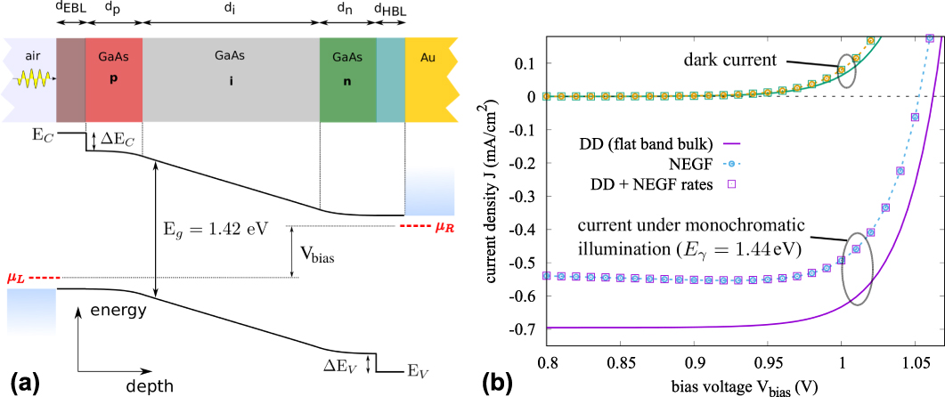
Recently, strongly enhanc to almost complete light absorption in ultra-scaled absorber layers with thicknesses in the deep sub-wavelength regime and nanophotonic light trapping has been shown both theoretically Reference Wang, White and Catchpole35,Reference Llorens, Buencuerpo and Postigo36 and experimentally. Reference Massiot, Colin, Péré-Laperne, Roca i Cabarrocas, Sauvan, Lalanne, Pelouard and Collin37–Reference Massiot, Vandamme, Bardou, Dupuis, Lemaitre, Guillemoles and Collin39 This opens up a route to highly efficient photovoltaic devices with vastly reduced material consumption and increased radiation tolerance. Reference Wang, Khan, Gray, Alam and Lundstrom40–Reference Hirst, Yakes, Warner, Bennett, Schmieder, Walters and Jenkins43 The understanding and design of quasi-confined or resonant optical modes is key to the realization of ultra-thin solar cells; however, the strong reduction of spatial extension also affects the electronic properties. While there is no heterostructure potential in the absorber region, the nonclassical contact regions occupy a significant fraction of the device and have a pronounced influence on the device characteristics. Figure 1(a) displays the structure of the ultra-thin GaAs p–i–n device under consideration here. The total thickness of the device is less than 100 nm. The light is incident from the left without any antireflection coating and is reflected at a gold mirror forming the right contact. The gold layer is considered explicitly only in the optical simulation. The optical model is based on the TMM in all cases, thus including the effects of multiple reflections. The optical rates and transport equations are computed either using the semiclassical formalism [Eqs. (4)–(9)] as implemented in the 1D thin-film solar cell simulator ASA, Reference Pieters, Krc and Zeman45 or the quantum-kinetic formalism [Eqs. (10)–(14)] for a two-band effective mass Hamiltonian. In the latter case, while the generation and recombination processes are enabled directly via the single particle interaction self-energies (16) and (17) for coherent and incoherent coupling to the (quantized) electromagnetic field, respectively, the representation of the optical rates as in (12) can be used to express the absorption coefficient in terms of microscopic quantities:
 $$\alpha \left( {z,{E_\gamma }} \right) \approx {{\hbar {c_0}} \over {6{n_{\rm{r}}}\left( {z,{E_\gamma }} \right){E_\gamma }}}\sum\limits_\mu \int{\mathop \smallint \nolimits {\rm{d}}z'{\mathop{\rm Re}\nolimits} \left[ {i{{\hat{\Pi }}_{\mu \mu }}\left( {{\bf{0}},z',z,{E_\gamma }} \right)} \right]} \quad,$$
where
 $$\Pi _{\mu \nu }^{\rm ≶} \left( {{\bf{q}}_{\parallel} ,z,z',E_\gamma } \right) = - i\hbar \mu _0 \left( {{e \over {m_0 }}} \right)^2 × p_{{\rm{cv}}}^{\mu * } \left( z \right)p_{{\rm{cv}}}^\nu \left( {z'} \right){\cal P}_{{\rm{cv}}}^≶ \left( {{\bf{q}}_{\parallel} ,z,z',E_\gamma } \right)\quad ,$$
is the photon self-energy for the electron–hole polarization function
 $${\cal P}_{{\rm{cv}}}^≶ \left( {{\bf{q}}_{\parallel} ,z,z',E_\gamma } \right) = {\cal A}^{ - 1} \sum\limits_{{\bf{k}}_{\parallel} } {\int {{{{\rm{d}}E} \over {2\pi \hbar }}G_{\rm{c}}^{\rm{≶}} \left( {{\bf{k}}_{\parallel} ,z,z',E} \right)G_{\rm{v}}^{\rm{\gtrless}} ×\left( {{\bf{k}}_{\parallel} - {\bf{q}}_{\parallel} ,z',z,E - E_\gamma } \right)\quad } } .$$
(a) Layer structure, doping levels and corresponding band profile of an ultra-thin GaAs p–i–n solar cell with carrier-selective contacts. Reference Aeberhard47 (b) Device characteristics of the solar cell device in (a) in the dark and under monochromatic illumination with photon energy E γ = 1.44 eV and intensity of 0.1 kW/m2. While there is a significant deviation of the NEGF result from the DD characteristics based on FBB material parameters, use of the NEGF rates in the DD formalism reproduces the full NEGF result, pointing at ideal carrier extraction. Adapted with permission from Refs. Reference Aeberhard47 and Reference Aeberhard48.

In the above equations, the slab representation adequate for planar geometries is used, with z denoting the perpendicular coordinate and k
‖ (q
‖) denoting the transverse momentum of electrons (photons) associated with the periodic in-plane dimensions. μ and ν are the polarization indices, μ0 is the vacuum permeability, p
cv is the interband momentum matrix element, and
 ${\cal A}$
is the transverse cross section. In terms of the photon self-energy and GF, i.e., in a picture that allows for a consistent description of absorption and emission, the absorptance appearing in the global DB limit acquires the form (
 $\hat{{\cal D}} \equiv {{\cal D}^ > } - {{\cal D}^ {\lt }$
,
 $\hat{\Pi } \equiv {\Pi ^ > } - {\Pi ^ {\lt }$
)
 $${a_{\mu \nu }}\left( {{{\bf{q}}_{\parallel} },{E_\gamma }} \right) = - \int {{\rm{d}}z} \int {{\rm{d}}z'\left[ {{{\hat{{\cal D}}}_{{\rm{v}},\mu \nu }}\left( {{{\bf{q}}_{\parallel} },z,z',{E_\gamma }} \right)×{{\hat{\Pi }}_{\nu \mu }}\left( {{{\bf{q}}_{\parallel} },z',z,{E_\gamma }} \right)} \right]} \quad .$$
In the same picture, the spectral emission rate corresponding to the integrand in the semiclassical expression (6) reads
 $$r^\mu \left( {{\bf{q}}_{\parallel} ,z,E_\gamma } \right) = \sum\limits_\nu {\int {{\rm{d}}z'\left( {2\pi \hbar } \right)^{ - 1} {\cal D}_{\mu \nu }^ > \left( {{\bf{q}}_{\parallel} ,z,z\prime ,E_\gamma } \right)×\Pi _{\nu \mu }^ {\lt }\left( {{\bf{q}}_{\parallel} ,z',z,E_\gamma } \right)\quad } } .$$
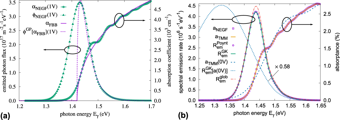
In the band profile displayed in Fig. 1(a), two salient features are the sizable bend bending due to the large built-in field, and the carrier-selective contacts imposed by blocking layers with potential barriers for minority carriers. Figure 1(b) displays the current–voltage characteristics for the case of perfect selectivity (ΔE C,V → ∞), in the dark and under monochromatic illumination at E γ = 1.44 eV and an intensity of 0.1 kW/m2. The sizable discrepancies in the dark and photocurrent between the semiclassical DD results and the NEGF characteristics are largely explained by the strong field effects on absorption and emission that lead to deviations from FBB properties regarding generation and recombination, as shown in Fig. 2(a) for the absorption coefficient and the emission rate at the center of the intrinsic region. In the FBB case, the following expression is used for the absorption coefficient:
 $$\alpha _{{\rm{bulk}}}^{{\rm{pb}}}\left( {{E_\gamma }} \right) = {{{{\left( {2m_{\rm{r}}^ * } \right)}^{{3 \over 2}}}} \over {2\pi {\hbar ^2}\sqrt {{\varepsilon _{\rm{b}}}} {\varepsilon _0}{c_0}{E_\gamma }}}{\left( {{e \over {{m_0}}}{p_{{\rm{cv}}}}} \right)^2}\sqrt {{E_\gamma } - {E_{\rm{g}}}} \Theta \left( {{E_\gamma } - {E_g}} \right)\quad,$$
with
 $m_{\rm{r}}^ *$
the reduced effective mass, εb the background dielectric constant, and E
g the band gap energy. Remarkably, if the NEGF rates (12) are used in semiclassical balance Eq. (7), the NEGF characteristics are reproduced. While the actual transport regime might still be very different in the two cases (ballistic extraction in the NEGF picture versus the diffusive band-like transport in the DD picture), the coincidence roots in perfect carrier extraction due to the long radiative lifetime.
Reference Aeberhard27
(a) Absorption coefficient and emission rate at the center of the intrinsic region, as provided by a flat-potential parabolic two-band bulk model (lines) using the Van Roosbroeck–Shockley formalism, and as obtained from the NEGF formalism (symbols) for the same two-band model, but including the actual band profile. (b) Absorptance and normal emission at the left surface of the solar cell, demonstrating the breakdown of the photovoltaic reciprocity between external quantum efficiency at zero bias voltage and luminescence emission at large forward bias: the strong modification of the absorptance with bias invalidates the use of the short circuit absorptance in the generalized Kirchhoff law for the emission. The difference in the emission with respect to the dash-dotted line corresponding to the integrated internal emission rate is a signature of photon recycling effects. Adapted with permission from Ref. Reference Aeberhard and Rau46.

As a direct consequence of the pronounced field effects, the large variation of the longitudinal field with terminal voltage V causes the breakdown of the superposition principle and, eventually, of the photovoltaic reciprocity relation
Reference Rau13
between photocurrent extraction—expressed by the external quantum efficiency—and the luminescent emission due to carrier injection under applied bias voltage. Figure 2(b) shows the change of the absorptance when going from short circuit conditions (V = 0 V) to large forward bias close to open circuit conditions (V = 1.1 V). The absorptance obtained from the GFs by the evaluation of Eq. (22) is in excellent agreement with the quantity directly obtained form the transfer-matrix model, which validates the photon GF approach.
Reference Aeberhard44
As demonstrated further in Fig. 2(b), the generalized Kirchhoff law for the emission spectrum based on the absorptance—i.e., Eq. (3)—applies only if the absorptance at the point of operation is used, while the emission based on the absorptance at V = 0 V exhibits a strong broadening and red shift. The difference between internal and external emissions caused by reabsorption becomes visible in Fig. 2(b), where the integrated (normal) emission rate is shown (
 $R_{{\rm{em}}}^{{\rm{glob}}}$
, dash-dotted line) together with the (normal) emission from the left surface.
Reference Aeberhard and Rau46
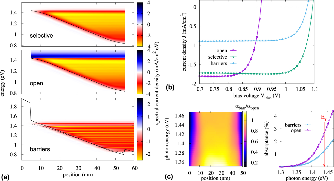
The second feature that is a characteristic for nanoscale absorbers concerns finite-size effects related to contact regions that span a nonnegligible fraction of the active device and have a measurable impact on the overall device performance. Reference Aeberhard47 Figure 3(a) displays the spectral current flow in a 50-nm ultra-thin device at 0.87 V of forward bias voltage under monochromatic illumination with E γ = 1.44 eV and at an intensity of 0.1 kW/m2. The three different contact configurations considered are ideally “selective” (ΔE C,V → ∞), “open” (ΔE C,V → 0), and with electron and hole “blocking layers” (EBL/HBL) inducing finite potential barriers at the contacts (0 < ΔE C,V < ∞). In the case of GaAs, suitable contact layers can be engineered using alloys, such as AlGaAs Reference Vandamme, Hung-Ling, Gaucher, Behaghel, Lemaitre, Cattoni, Dupuis, Bardou, Guillemoles and Collin42 or InGaP, Reference Yang, Becker, Liu, Kuo, Li, Landini, Campman and Zhang41 or a combination thereof. Reference Cavassilas, Gelly, Michelini and Bescond26 The ideally selective contact blocks reverse the current flow—i.e., leakage current—of minority carriers completely, while majority carriers are extracted without barrier. In the absence of the barrier for minority carriers (open contact), carriers that are injected at the majority carrier contact or photogenerated inside the intrinsic region can leave the device via the minority carrier contact, which represents a significant leakage loss. In the case of photocurrent leakage, the short circuit current is reduced, while the leakage of electrically injected carriers contributes to the dark saturation current and hence results in a reduction of open circuit voltage V OC. Figure 3(b) displays the current–voltage characteristics of the different contact configurations. While the loss in V OC is explained by the dark current due to the leakage as discussed above, the reduction of short circuit current J SC in the presence of the blocking layers is due to the appearance of nonclassical regions of reduced density of states in close proximity of the barriers, which translates to a reduced absorption coefficient [Fig. 3(c)]. In the case of simultaneous presence of electron and hole blocking layers with finite barriers also for majority carriers, size quantization enhances this effect and leads to both a resonance structure in the spectral current and a strongly reduced absorptance at photon energies close to the band gap, as shown in Fig. 3(c).
(a) Spectral current flow in a 50-nm thick p–i–n photodiode with perfectly selective, open and blocking layer contacts, respectively. The open contact configuration leads to pronounced leakage losses at forward bias in the form of a negative current component at energies above the edge at the left contact. Blocking layers (barriers) at both contacts, on the other hand, prevent leakage but induce size quantization effects. (b) Current–voltage characteristics for the different configurations: for open contacts, leakage losses result in strong reduction of the open circuit voltage, while contact barriers lead to a reduction in short circuit current. (c) Short circuit current losses induced by barriers are the consequence of reduced absorption due to the appearance of nonclassical regions of reduced density of states in the vicinity of the barriers. Adapted with permission from Ref. Reference Aeberhard47.

B. QWSCs
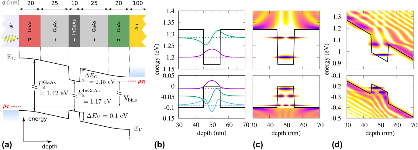
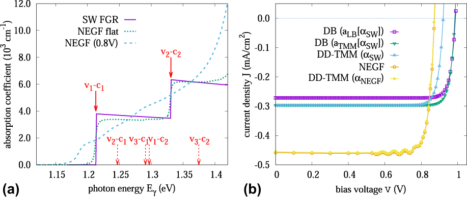
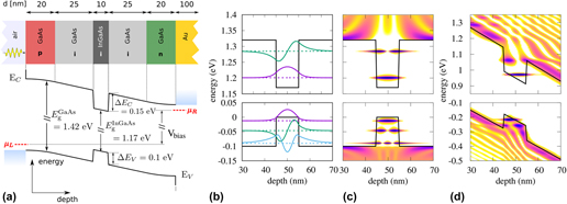
QWSCs have been introduced as tunable band gap absorbers in single and multijunction configurations. Reference Barnham and Duggan1,Reference Ekins-Daukes, Barnes, Barnham, Connolly, Mazzer, Clark, Grey, Hill, Pate and Roberts49 Advanced strain-balancing approaches allow for the exploitation of a large material parameter space while keeping the density of structural defects low. Reference Ekins-Daukes, Barnham, Connolly, Roberts, Clark, Hill and Mazzer50 In QWSCs, the absorber contains the regions of lower dimensional electronic states that are partially confined in transport direction owing to the variation in band gap and electron affinity of the constituent bulk materials. In conventional multiquantum-well architectures, the quantum-well states are not directly coupled to the contacts, and carriers generated in such localized states have to be transferred to extended continuum states prior to extraction. Reference Aeberhard51,Reference Aeberhard52 The escape of carriers proceeds via thermionic emission, direct-, or phonon-assisted tunneling, depending on the temperature, injection level, and strength of the built-in field. The situation is different in superlattices of strongly coupled QW, Reference Wang, Watanabe, Wen, Sugiyama and Nakano53 where extraction proceeds via confined states related to miniband formation, with transport regimes ranging from ballistic escape to sequential tunneling assisted by phonon emission. Reference Aeberhard22,Reference Aeberhard54 Here, to investigate the impact of the additional deviation from an ultra-thin, but otherwise homogeneous bulk-like absorber, we study a GaAs p–i–n photodiode with a single InGaAs quantum well embedded in the intrinsic region, as displayed in Fig. 4(a). As in the case of the ultra-thin absorber device, the light is incident from the left, and the gold reflector is considered in the optical simulation only. In Fig. 4(b), the envelope functions of confined electron and hole states of the field-free quantum well as obtained by solving the effective mass Schrödinger equation with closed-system (Dirichlet) boundary conditions are shown. The corresponding local density of states provided by the NEGF formalism based on the same effective mass Hamiltonian at flat-band conditions is displayed in Fig. 4(c). This time, the local density of state (LDOS) includes the perturbed continuum above the well, featuring quasi-continuum states that give rise to transmission resonances. While the flat-band NEGF picture coincides with the closed-system Schrödinger picture for the confined states in terms of resonance energy and spatial variation, the NEGF LDOS for the self-consistent potential at the operating point of 0.8 V of forward bias voltage exhibits strong field effects in terms of Stark shifts and partial unbinding of the higher confinement levels [Fig. 4(d); please note the difference in energy scale with respect to (b) and (c)]. Following the derivation of the states in the square-well (SW) potential under vanishing and self-consistent field, a similar analysis is performed for the absorption coefficient; Fig. 5(a) displays the textbook absorption coefficient as obtained from the FGR rate based on the flat-band SW potential states,
 $${\alpha _{{\rm{SW}}}}\left( {{E_\gamma }} \right) = f \cdot E_\gamma ^{ - 1}\sum\limits_{i,j} {{{\left| {{M_{{{\rm{c}}_i}{{\rm{v}}_j}}}} \right|}^2}\Theta \left( {{E_\gamma } - {\varepsilon _{{{\rm{c}}_i}{{\rm{v}}_j}}}} \right)\quad,}$$
with Θ the unit step function and
 $$f = {{{e^2}m_{\rm{r}}^ * P_{{\rm{cv}}}^2} \over {m_0^2\hbar {n_{\rm{r}}}{c_0}{\varepsilon _0}{L_{\rm{w}}}}}\quad,$$
where
 $m_{\rm{r}}^ *$
is the reduced effective mass,
 ${P_{{\rm{cv}}}} = \sqrt {{E_{\rm{P}}}{m_0}{\rm{/}}6}$
is the bulk momentum matrix element for Kane energy E
P = 26.9 eV, n
r = 3.7 is the refractive index of the bulk material, and c
0 and ε0 are speed of light and permittivity in vacuum, respectively. The overlap matrix elements
 $${M_{{{\rm{c}}_i}{{\rm{v}}_j}}} = \int_L {{\rm{d}}z\psi _{{{\rm{c}}_i}}^ * \left( z \right){\psi _{{{\rm{v}}_j}}}\left( z \right)\quad },$$
where L(>L w) is the normalization length of the envelope functions in z-direction ψ, introducing the optical selection rules according to the WF symmetry that suppress a number of transitions as indicated by dashed arrows. The NEGF absorption coefficient, which is related to the LDOS in Fig. 4(c), reproduces the FGR result, up to the effects of finite broadening but including the selection rules, which is a highly nontrivial result, as it requires the consideration of the full nonlocality in the evaluation of the joint density of states encoded in the polarization function (21). Reference Aeberhard55 However, the NEGF absorption coefficient based on the LDOS in Fig. 4(d) bears little resemblance to the SW flat-band absorption, as the strong field leads to a pronounced red shift of the absorption edge and to a relaxation of selection rules due to symmetry breaking, while the unbinding of states removes the 2D character of the (joint) density of states. In the global DB and the semiclassical picture, the absorption coefficient is the main ingredient for the computation of the current–voltage characteristics of the device at the radiative limit. In the former case, it is used for the computation of the absorptance in Eqs. (2) and (3), while in the latter, it provides the generation and recombination rates via Eqs. (5) and (6), respectively. In Fig. 5(b), the characteristics are shown for monochromatic illumination with E γ = 1.3 eV and at an intensity of 0.1 kW/m2 for different theoretical descriptions: the global DB picture with absorptance from LB law or the TMM for SW absorption coefficient (αSW); the semiclassical DD–Poisson model coupled to TMM; and the full NEGF–Poisson model. The LB and TMM pictures provide slightly different absorptance levels, and the DD model exhibits an increased dark saturation current due to the emission into the full solid angle as compared with the loss cone in the case of the global models and the absence of photon recycling. Remarkably, consideration of the absorption coefficient αNEGF as provided by the NEGF formalism results in semiclassical characteristics that match closely those of the full NEGF model. This justifies a posteriori the assumption of unit escape probability of carriers generated in quantum-well states that are used in the semiclassical model, which is based on experimental observations for device operation at room temperature and moderate well depth. Reference Nelson, Paxman, Barnham, Roberts and Button56 As in the case of the ultra-thin absorber, this unit extraction efficiency is, here, a consequence of the long radiative lifetime, such that the escape is much faster than the recombination. In reality, the escape competes with much faster nonradiative recombination channels, which in deep wells and at large forward bias corresponding to low fields results in incomplete carrier extraction. Furthermore, in a proper treatment of the charge density component related to confined states, accumulation of charge in the QW will have effects on both the electrostatic potential as well as the recombination rate. If the confinement is neglected, as in the semiclassical approach used here, carriers are generated in extended states only and drift or diffuse away quickly.
(a) Structure and band profile of a GaAs p–i–n photodiode with a single InGaAs quantum-well embedded in the intrinsic region. (b) Confined states in the QW for flat-band potential, as provided by the solution of the effective mass Schrödinger equation with closed-system boundary conditions. (c) Corresponding local density of states obtained from the NEGF formalism. (d) LDOS for the self-consistent potential at a forward bias of 0.8 V, i.e., close to the maximum power point. The deviation from flat-band potential leads to Stark shifts and partial unbinding of the QW states.

(a) Absorption coefficient of the single quantum-well photodiode in the energy range below the bulk band gap of the host material, for the three cases displayed in Fig. 4: from the FGR rate using the flat-band SW potential states, from NEGF for flat band, and from NEGF for the self-consistent potential at 0.8 V. While the NEGF absorption coefficient reproduces the FGR result up to some broadening effects, including the symmetry-induced selection rules, the absorption coefficient at 0.8 V exhibits a pronounced red shift, relaxation of selection rules due to symmetry breaking and deviation from purely two-dimensional density of states. (b) Current–voltage characteristics of the single quantum-well photodiode for monochromatic illumination with E γ = 1.3 eV and at an intensity of 0.1 kW/m2, as provided by the DB picture with absorptance from LB law or the TMM for SW absorption coefficient (αSW); the semiclassical DD–Poisson model coupled to TMM; and the full NEGF–Poisson model. While the LB and TMM laws provide slightly different absorptance levels, consideration of the absorption coefficient as provided by the NEGF formalism results in semiclassical characteristics that match closely those of the full NEGF model.

C. Quantum dot solar cells
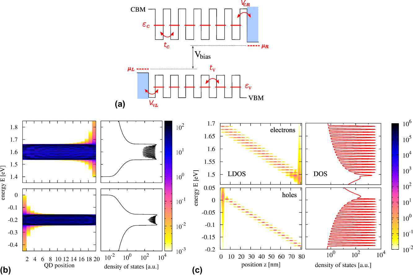
In quantum dots, the deviation from bulk material properties is maximum due to confinement induced by inhomogeneity in all three spatial dimensions. There is a large variety of quantum-dot architectures studied for photovoltaic applications, ranging from hybrid organic–inorganic bulk heterojunction type solar cells based on colloidal nanoparticle to superlattices of epitaxially grown QD of regular shape. Reference Nozik58–Reference Nozik, Beard, Luther, Law, Ellingson and Johnson60 Here, the focus is set on regimented arrays of inorganic low band gap nanoparticles embedded in a wide band gap host material, which enable the formation of extended states due to strong coupling of adjacent nanoparticles and have been investigated for applications as tunable band gap absorbers in tandem configuration Reference Jiang and Green61,Reference Conibeer, Green, Cho, König, Cho, Fangsuwannarak, Scardera, Pink, Huang, Puzzer, Huang, Song, Flynn, Park, Hao and Mansfield62 or for intermediate band solar cells. Reference Marti, Cuadra and Luque4 Figure 6(a) shows a schematic representation of an effective mesoscopic model of such an array, furnished with on-site energies, interdot hopping constants and a term describing the coupling to carrier-selective contacts. Reference Berbezier and Aeberhard25 Contact selectivity is essential to ensure charge separation close to flat-band conditions. Since atomistic resolution is out of discussion for extended arrays, a coarse grained localized basis approach is chosen where the QD wave functions are expressed in terms of QD orbitals. This amounts to field operators of the form
 $$\hat{\Psi }\left( {{\bf{r}},t} \right) = \sum\limits_{\nu,i} {{\psi _{\nu,i}}\left( {\bf{r}} \right){{\hat{d}}_{\nu,i}}\left( t \right)\quad },$$
with ψ the QD orbital wave function and
 ${\hat{d}_{\nu,i}}$
the annihilation operator for electrons in QD orbitals ν at QD site i. In this basis, the model corresponds to a simple nearest-neighbor tight-binding chain of finite length expressed by the Hamiltonian
 $$\hat{{\cal H}}_0^\nu = \sum\limits_{i = 1}^{{N_{{\rm{QD}}}} - 1} {{t_{\nu,ii + 1}}\left[ {\hat{d}_{\nu,i + 1}^\dag {{\hat{d}}_{\nu,i}} + {\rm{h}}{\rm{.c}}{\rm{.}}} \right]} + \sum\limits_{i = 1}^{{N_{{\rm{QD}}}}} {{\varepsilon _{\nu,i}}{{\hat{n}}_{\nu,i}}} \quad,$$
where N
QD is the number of dots, t
ν is the interdot coupling,
 ${\hat{n}_\nu } \equiv \hat{d}_\nu ^\dag {\hat{d}_\nu }$
is the carrier density operator, and εν is the QD energy level. The dot-contact coupling is considered in the usual way by means of a contact self-energy that vanishes for closed contacts. The strength of the coupling
 ${\cal T}$
in the expression for the contact self-enery is given in terms of the parameter V
B, with B = cR and B = vL for selective coupling of electrons to the right contact and holes to the left contact. In the flat-band case displayed in Fig. 6(b), the coupling of the dots leads to the delocalization of the wave functions over the entire array. At the contacts, the hybridization of the dot states with the electrode induces a broadening of the LDOS, corresponding to the reduction of lifetime due to carrier escape to the contacts. In the presence of strong built-in fields, the wave functions localize over a limited number of neighboring quantum dots, which slows down carrier extraction due to the requirement of sequential carrier relaxation processes.
Reference Aeberhard24
This is shown in Fig. 6(c) for the case of a heterosuperlattice of silicon quantum dots laterally confined in silicon oxide and vertically separated by barrier layers of silicon carbide.
Reference Ding, Aeberhard, Astakhov, Köhler, Beyer, Finger, Carius and Rau63
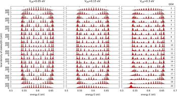
Even at flat-band conditions, the site-resolved LDOS is not uniform throughout the finite-size array, as shown in Fig. 7 for the lowest electron miniband in a 20 QD array with contact to dot number 20. For strong dot-contact coupling V
cR, the states in the vicinity of the contact are renormalized, which amount to a shift to lower energies and result in the formation of a strongly localized surface state. The impact of interdot and dot-contact coupling parameters t
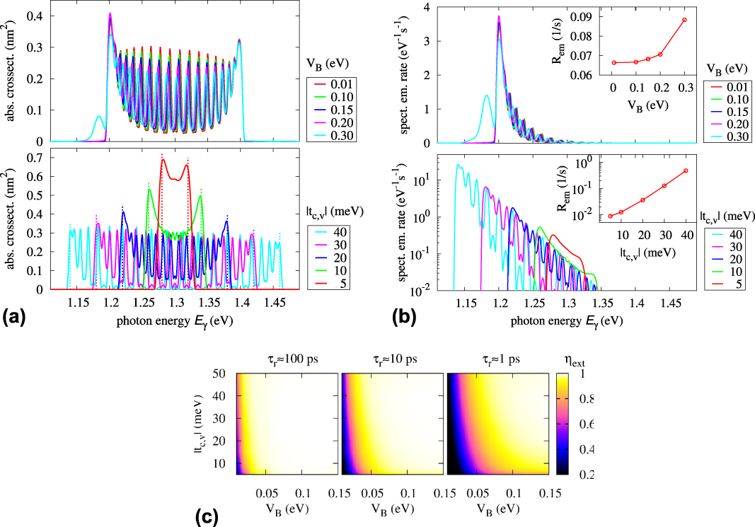
c,v and V
B (B = cR, vL) on the radiative rates is shown in Figs. 8(a) and 8(b) displaying the absorption cross section and the spectral emission rate of the 20 QD array for different values of the coupling parameters. Up to the critical contact coupling where surface states are formed, the main impact of the contact is to induce a slight broadening to the contributions of the individual dots to the spectra. The interdot coupling, on the other hand, determines the bandwidth of the spectral response, which in turn has a pronounced effect on the magnitude of the emission via the size of the effective band gap. To study the impact of configurational parameters on the efficiency of photocarrier extraction, the ratio ηext = J
SC/J
abs of short circuit current to generation current as obtained from the absorption cross section is evaluated for different values τr of radiative lifetime and coupling parameters. As shown in Fig. 8 for a 20 QD array at flat-band conditions and under monochromatic resonant excitation with the central frequency of the miniband, it is the contact coupling that limits the performance in all situations, while the interdot coupling becomes critical only at very low photocarrier lifetime.
Reference Berbezier and Aeberhard25
(a) Schematic representation of a mesoscopic model for quantum-dot array solar cells, including on-site energy, interdot hopping and coupling to carrier-selective contacts. (b) LDOS of the lowest electron and hole minibands for a 20 QD array at vanishing field, where the states extend over the entire array. Hybridization with the bulk electrode induces strong broadening of the LDOS at the contacts. (c) In the presence of finite built-in fields, the minibands break up and the wave functions localize over a few neighboring QD. This has a potentially detrimental impact on the carrier extraction efficiency, as sequential relaxation processes are required for transport to the contacts. Adapted with permission from Refs. Reference Berbezier and Aeberhard57 and Reference Aeberhard24.

LDOS of the lowest electron “miniband” of a 20 QD array with selective contact to the dot number 20. Even at low dot-contact coupling, the finite size of the array results in a spatial variation of the site-resolved LDOS. Increasing dot-contact coupling induces a renormalization of the states adjacent to the contact, which results in a shift to lower energies and formation of a strongly localized surface state. Reprinted with permission from Ref. Reference Berbezier and Aeberhard57.

(a) Absorption cross section and (b) spectral emission rate for a 20 QD array with varying values of interdot coupling t c = t v and dot-contact coupling V B = V cR ≡ V vL. The contact contributes primarily a broadening up to very strong coupling, where a localized surface state is induced. The interdot coupling affects the bandwidth of the spectral response, including the size of the effective gap which has a strong impact on the magnitude of the emission. (c) Photocarrier extraction efficiency in a 20 QD array as a function of configurational parameters (interdot coupling t c,v, dot-contact coupling V B) and carrier recombination lifetime τr. The dot-contact coupling limits the extraction efficiency, while interdot coupling becomes critical only for very low lifetime. Adapted with permission from Ref. Reference Berbezier and Aeberhard57.

IV. SUMMARY AND CONCLUSIONS
The operation of nanostructure-based photovoltaic devices exhibits substantial deviations from bulk physics, not only regarding the electronic, optical, and vibrational structure, but also in the dynamical processes involving nanostructure states. As a consequence, the device characteristics are determined by the operating conditions and inhomogeneities in structure and composition as well as finite-size and surface effects rather than by the flat-band bulk properties of the constituent materials. The semiclassical macroscopic bulk picture conventionally used for the simulation of photovoltaic device characteristics fails to capture many of these effects by default. On the other hand, a microscopic generalization of the steady-state balance equations on the level of quantum statistical mechanics is able to provide a comprehensive quantum theory of photovoltaics at the nanoscale. This allows us to assess on physical grounds the impact of configurational parameters on the photovoltaic device performance. Comparison of the predictions based on the different simulation approaches shows that in situations where transport is mediated by extended bulk states, consideration of the actual density of states at the operating point for the evaluation of the optical rates used in the semiclassical balance equations is sufficient to obtain the correct characteristics. The effects of potential barriers on charge extraction, on the other hand, still require the full evaluation of the quantum transport problem. In general, a comprehensive and accurate, but still efficient assessment of nanostructure solar cell devices based on simulation will require a multiscale simulation framework relying on suitable combinations of the modeling approaches discussed in the present work. At this point, it is indicated to point out that nonclassical regions in solar cells are not restricted to nanostructure-based devices but appear in the form of interface and heterocontact regions in a large variety of applications, from the a-Si:H/c-Si interface of the silicon heterojunction solar cell to grain boundaries and selective contacts in perovskite devices. The advanced theoretical analysis proposed here has thus applications in a wide range of current photovoltaic device research activities.
ACKNOWLEDGMENT
This work has benefited from fruitful discussions within COST action MP1406 – MultiscaleSolar.