I. INTRODUCTION
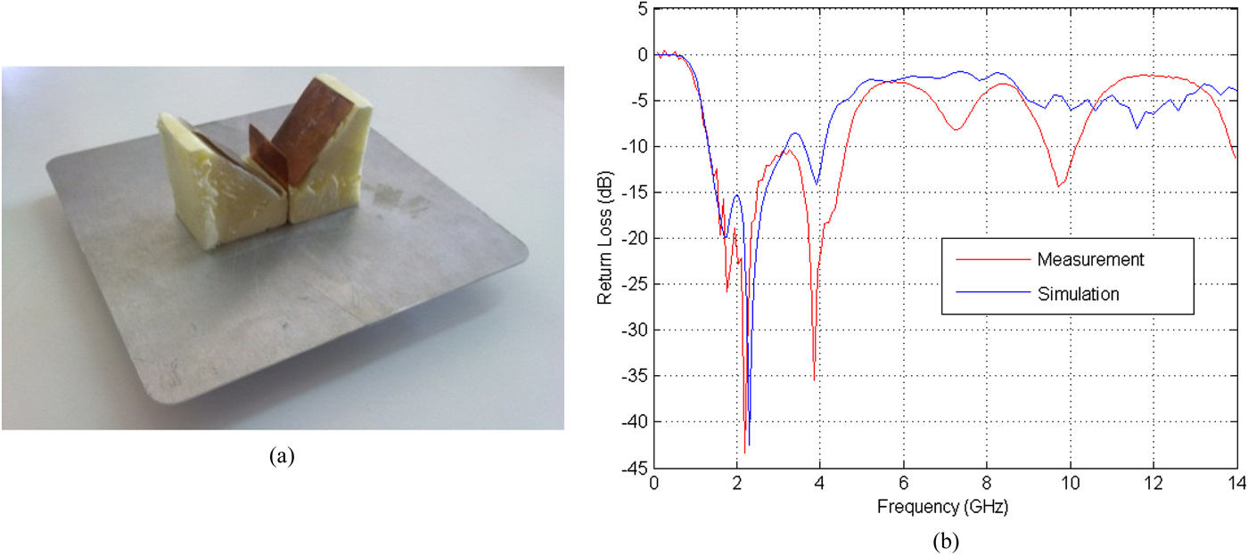
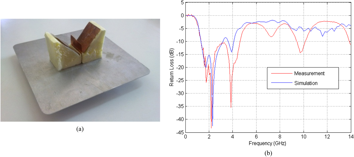
Increasing demand for higher data rates in most recent wireless communication applications require ultra wideband (UWB) antennas. Broadband monopole antennas have appealing features such as wide frequency band, compactness, low-cost, simple structure, light weight, and ease of manufacture [Reference Dastranj, Imani and Hassani1]. Printed circuit board (PCB) in many different shapes such as circular, square, elliptical, and triangle are also constructed and proposed for UWB applications to operate over a very wide band in 2.6–14.3 GHz [Reference Ren, Deng and Chen2]. In a recent work, it is reported that a square planar monopole antenna with a V-shaped coupling element (V-shaped square planar monopole antenna (V-SPMA)), seen in Fig. 1, could become a very satisfactory candidate as an UWB antenna, which can cover many communication standards such as cellular phone systems (900 MHz, 1800/1900 MHz) as well as 3 G (2.1–2.6 GHz), and Wi-Fi (2.4 and 5.2 GHz) frequency bands [Reference Karakus, Aydin, Atilla, Nesimoglu and Yarman3]. Using such a single V-shaped SPMA in a wireless system could decrease the problems such as system complexities, high costs, high circuitry areas, high DC power consumption caused by many separate narrow-band antennas, and its accompanying matching elements. In [Reference Karakus, Aydin, Atilla, Nesimoglu and Yarman3], it is reported that the V-SPMA antenna is manufactured, measured, and extensively worked on its performance from the usability point of view as an UWB antenna for the above-mentioned communication bands.
(a) Constructed prototype of the V-SPMA antenna, (b) measured and simulated return loss results for the V-SPMA [3].
Owing to difficulties of making antenna, the antenna designer has not always the opportunity to attain a flat power transfer characteristics which is a very desirable feature for maximum power transfer within the usable operating band of the antenna. For the purpose of flattening the in-band power gain characteristics of V-SPMA as much as possible, a matching network design is done. A very well-known, highly successful, and commonly used design approach called “real frequency technique” (RFT) is preferred as the design tool, since it has a feature of yielding always convergent solution over an UWB coverage [Reference Köprü, Kuntman and Yarman4–Reference Yarman6] when equipped with proper non-linear optimization algorithms [Reference Chen, Jiang, Chen and Zhang7, Reference Lagarias, Reeds, Wright and Wright8]. In the work, RFT uses input reflectance data S 11 given for the V-SPMA antenna in 40 MHz–14 GHz frequency range to able to obtain an eight-element Butterworth-type bandpass matching network (BPMN). BPMN is designed using a Matlab [9] code inside, which RFT runs and the resulting circuit is simulated in MicroWave Office (MWO) of AWR Corporation [10].
II. MATCHING NETWORK DESIGN USING REAL FREQUENCY DIRECT COMPUTATIONAL TECHNIQUE (RFDCT)
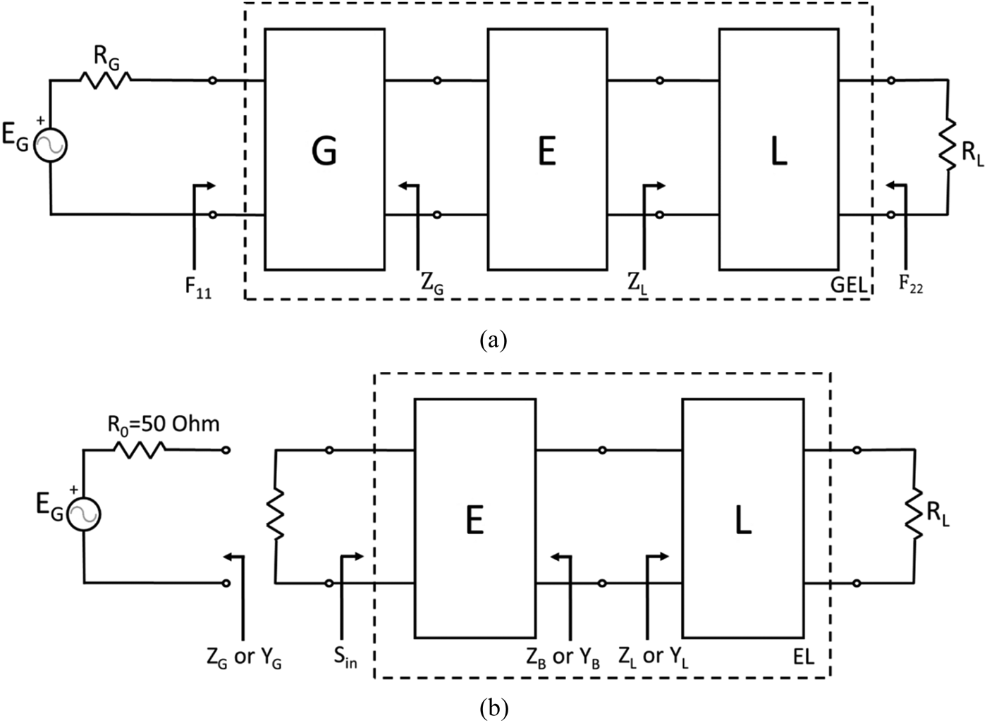
Matching network design is preferred to be done using “RFDCT” in which transducer power gain (TPG) of the double matched system seen in Fig. 2 is described in terms of the driving point immitances of the generator [Z G or Y G ], equalizer (antenna matching network, BPMN) [Z B or Y B ] and the load (V-SPMA antenna) [Z L or Y L ]. TPG for the V-SPMA antenna matching problem is given as [Reference Yarman5]
 $$T=\displaystyle{{1 - {{\left\vert {{G_{22}}} \right\vert }^2}} \over {{{\left\vert {1 - {G_{22}}{S_{in}}} \right\vert }^2}}}{T_{EL}}.$$
(a) Double matching problem, (b) cascaded connection of two lossless two-ports [G] and [EL].
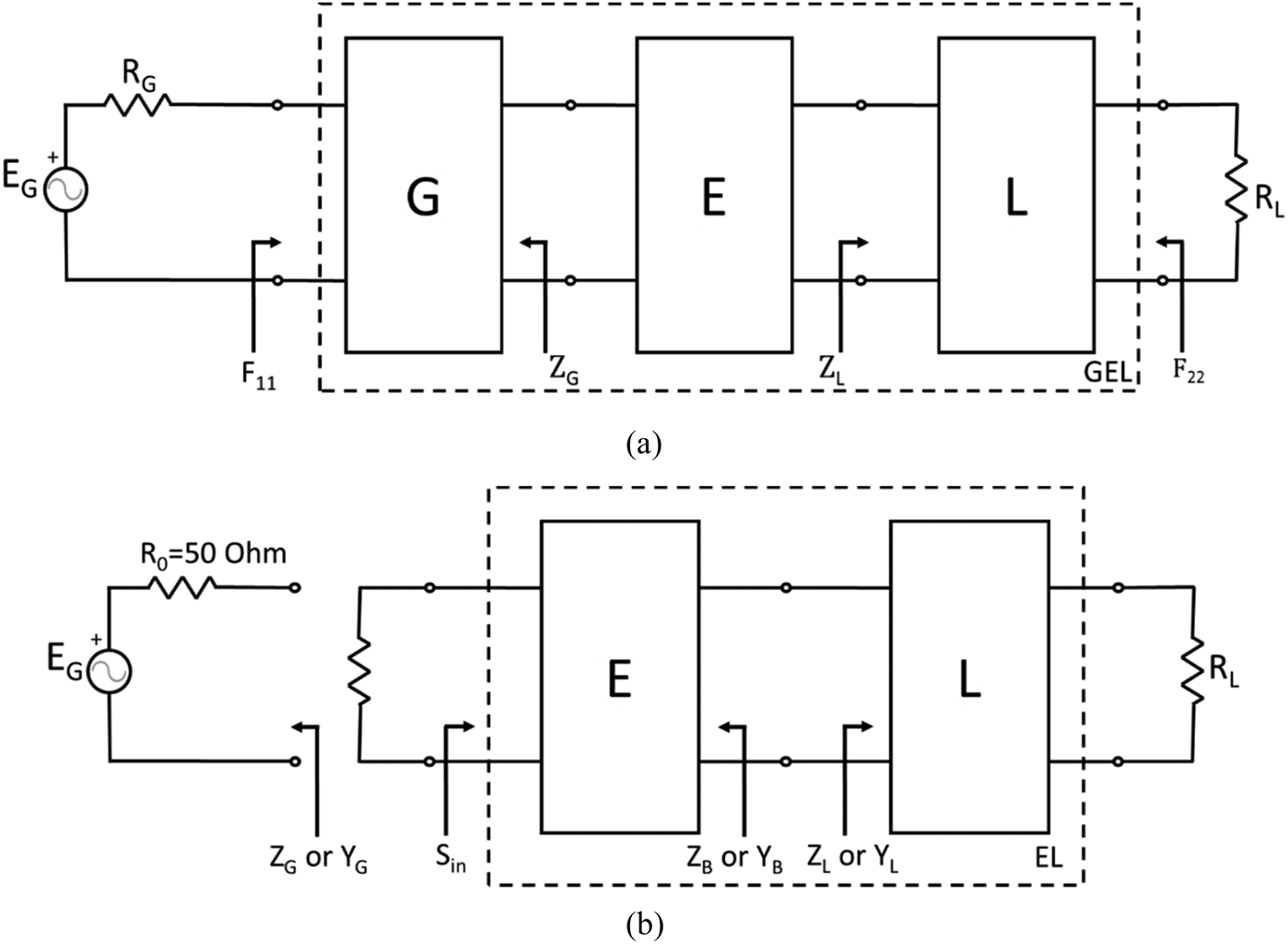
In terms of the standard normalization resistor R 0 = 50 Ω, unit normalized generator reflectance G 22 and input reflectance S in of [EL] structure are given, respectively, by
 $${G_{22}}=\displaystyle{{{Z_G} - {R_0}} \over {{Z_G}+{R_0}}}\comma \;$$
 $${S_{in}}={\eta _B}\displaystyle{{{Z_L}\lpar j\omega \rpar - {Z_B}\lpar - j\omega \rpar } \over {{Z_L}\lpar j\omega \rpar +{Z_B}\lpar - j\omega \rpar }}\comma \;$$
where Z L (jω) is the input impedance data of the V-SPMA antenna to be computed by using its given input reflectance data S 11(jω) over the frequency band of interest as
 $${Z_L}\lpar j\omega \rpar ={R_0}\displaystyle{{1+{S_{11}}\lpar j\omega \rpar } \over {1 - {S_{11}}\lpar j\omega \rpar }}.$$
Z B (jω) is the back-end impedance of the [E] equalizer (BPMN) to be computed by
 $${Z_B}\lpar p\rpar =\displaystyle{{{a_1}{p^n}+{a_2}{p^{n - 1}}+\cdots+{a_n}p+{a_{n+1}}} \over {{b_1}{p^n}+{b_2}{p^{n - 1}}+\cdots+{b_n}p+{b_{n+1}}}}\comma \; \; \quad p=j\omega\comma \;$$
where p = jω is the Laplace variable. Z B (p) is a positive real (PR) impedance function that is to be determined in the optimization process. The all pass function η B (p) is given as
 $${\eta _B}\lpar p\rpar ={\lpar \!-\! 1\rpar ^{{n_{dc}}}}\displaystyle{{b\lpar \!-\! p\rpar } \over {b\lpar p\rpar }}\comma \;$$
where n dc is the number of transmission zeros at DC. The TPG T EL of the lossless two port [EL], which is composed of matching network and the antenna is given by [Reference Yarman5]
 $${T_{EL}}\lpar \omega \rpar =1\! -\! {\left\vert {{S_{in}}\lpar j\omega \rpar } \right\vert ^2}=\displaystyle{{4{R_B}\lpar p\rpar {R_L}\lpar j\omega \rpar } \over {{{\left\vert {{Z_B}\lpar p\rpar +{Z_L}\lpar j\omega \rpar } \right\vert }^2}}}\comma \; \quad p=j\omega\comma \;$$
where R L and X L are real and imaginary parts of the antenna input impedance Z L (jω), respectively. R B is the real or resistive part of back-end impedance function Z B (p) and it is given by [Reference Yarman5]
 $$\eqalign{{R_B}\lpar {p^2}\rpar &=Even\left\{{{Z_B}\lpar p\rpar } \right\}\cr &=\displaystyle{{{A_0}{p^{2{n_{dc}}}}} \over {{B_1}{p^{2n}}+{B_2}{p^{2\left({n - 1} \right)}}+\cdots+{B_n}{p^2}+1}} \cr &=\displaystyle{{A\lpar {p^2}\rpar } \over {B\lpar {p^2}\rpar }} \geq 0\comma \; \forall \omega\comma \; }$$
where the denominator is an even polynomial given by B(p
2) = 1/2[c(p)2 + c(−p)2], which is formed with an auxiliary polynomial
 $c\left(p \right)={c_1}{p^n}+{c_2}{p^{n - 1}}+\cdots+{c_n}p+1$
. Once the auxiliary polynomial coefficients {c
i
; i = 1, 2, …, n} and
 ${A_0}=a_0^2 \geq 0$
of the real part R
B
(ω) are initialized, we can generate the error function ε as follows [Reference Yarman5]:
 $$\eqalign{{\varepsilon _i} &=T\lpar {p_i}\rpar - {T_t}\lpar {p_i}\rpar \cr & =\displaystyle{{1 - {{\left\vert {{G_{22\comma i}}} \right\vert }^2}} \over {{{\left\vert {1 \!-\! {G_{22\comma i}}{S_{in\comma i}}} \right\vert }^2}}}{T_{EL}} - {T_t}\lpar {p_i}\rpar \cr &=\displaystyle{{1 - {{\left\vert {{G_{22\comma i}}} \right\vert }^2}} \over {{{\left\vert {1 - {G_{22\comma i}}{S_{in\comma i}}} \right\vert }^2}}}\left\{{\displaystyle{{4{R_B}\lpar {p_i}\rpar {R_{L\comma i}}} \over {{{\left\vert {{Z_B}\lpar {p_i}\rpar +{Z_{L\comma i}}} \right\vert }^2}}}} \right\}- {T_t}\lpar {p_i}\rpar \comma \cr &{\rm for}\left\{{i=1\comma \; 2\comma \; {\rm \ldots }\comma \; nd\, \, {\rm and}\, \, {p_i}=j{\omega _i}} \right\}\comma \; }$$
where nd is the number of frequency data uniformly distributed within the optimization band. T t (p) is a mathematically generated Butterworth or Chebyshev-type bandpass gain function to be used as the objective or target function curve to be tracked by the optimization algorithm such that
 $$\eqalign{&{T_t}\lpar {p^2}\rpar = \cr &\quad \left\{\matrix{ {T_{bw}}\lpar {p^2}\rpar \comma \; {\rm Butterworth}\, {\rm type}\, {\rm bandpass}\, {\rm target}\, {\rm gain}\, {\rm function} \cr T_{ch}\lpar {p^2}\rpar \comma \; {\rm Chebyshev}\, {\rm type}\, {\rm bandpass}\, {\rm target}\, {\rm gain}\, {\rm function} \cr} \right..}$$
The sole purpose of the above formulated process is to determine the Z B (p) = a(p)/b(p) impedance function as a realizable PR function belonging to the equalizer [E], i.e. the BPMN, by minimizing the error function (9.i) in a non-linear optimization process. Then, the corresponding LC lossless ladder network with resistive termination is obtained by applying the very well-known long division process to the Z B (p) function. Resistive termination is replaced by an ideal transformer with transformer ratio [R = n 2:1] which completes the design [Reference Yarman5].
Design steps in Matlab code:
-
• Enter the element number n of the BPMN to be designed.
-
• Enter normalized frequencies ω s 1, ω c 1, ω c 2, ω s 2 (lower stopband, lower corner, upper corner, upper stopband frequencies) to be used in constructing the Butterworth (or Chebyshev) template or target gain function of order 2n, T t (p 2) as given in (9.ii).
-
• Set
 $c=\left\{{{c_1} {c_2} \cdots {c_n} 1} \right\}$
and a
0 with arbitrary real numbers and construct the optimization initial vector by combination of both as x
0 = [ca
0].
-
• Execute an optimization function equipped by a suitable nonlinear optimization algorithm such that x = OptAlgorithm(‘OptFunc.m’, x 0, options); OptAlgorithm could be chosen as lsqnonlin or fminsearch. Corresponding line is then typed as x = lsqnonlin(‘OptFunc.m’, x0 , options); OR x = fminsearch(‘OptFunc.m’, x 0, options);
-
• Execute OptFunc.m, to minimize the error function given in (9.i).
-
• After obtaining the solution vector x = [ca 0] via a successful optimization, construct A(p 2) and B(p 2) even polynomials as in (8) using the scalar a 0 and the vector [c].
-
• Determine Z B (p) = a(p)/b(p) input impedance of the antenna matching network (equalizer [E]), i.e. BPMN, and synthesize it to obtain the resulting LC lossless ladder network.

III. SIMULATION RESULTS
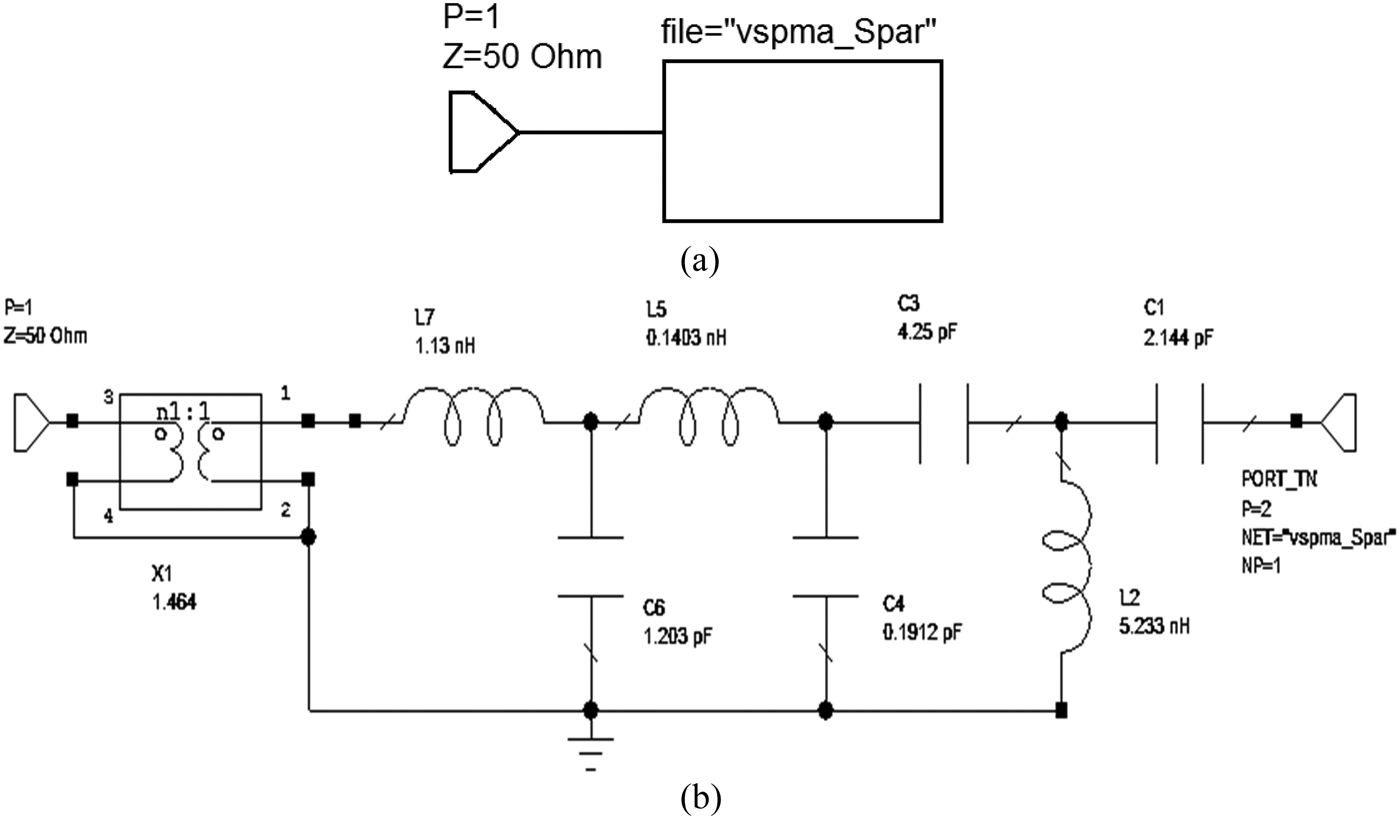
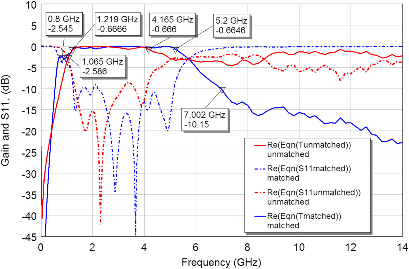
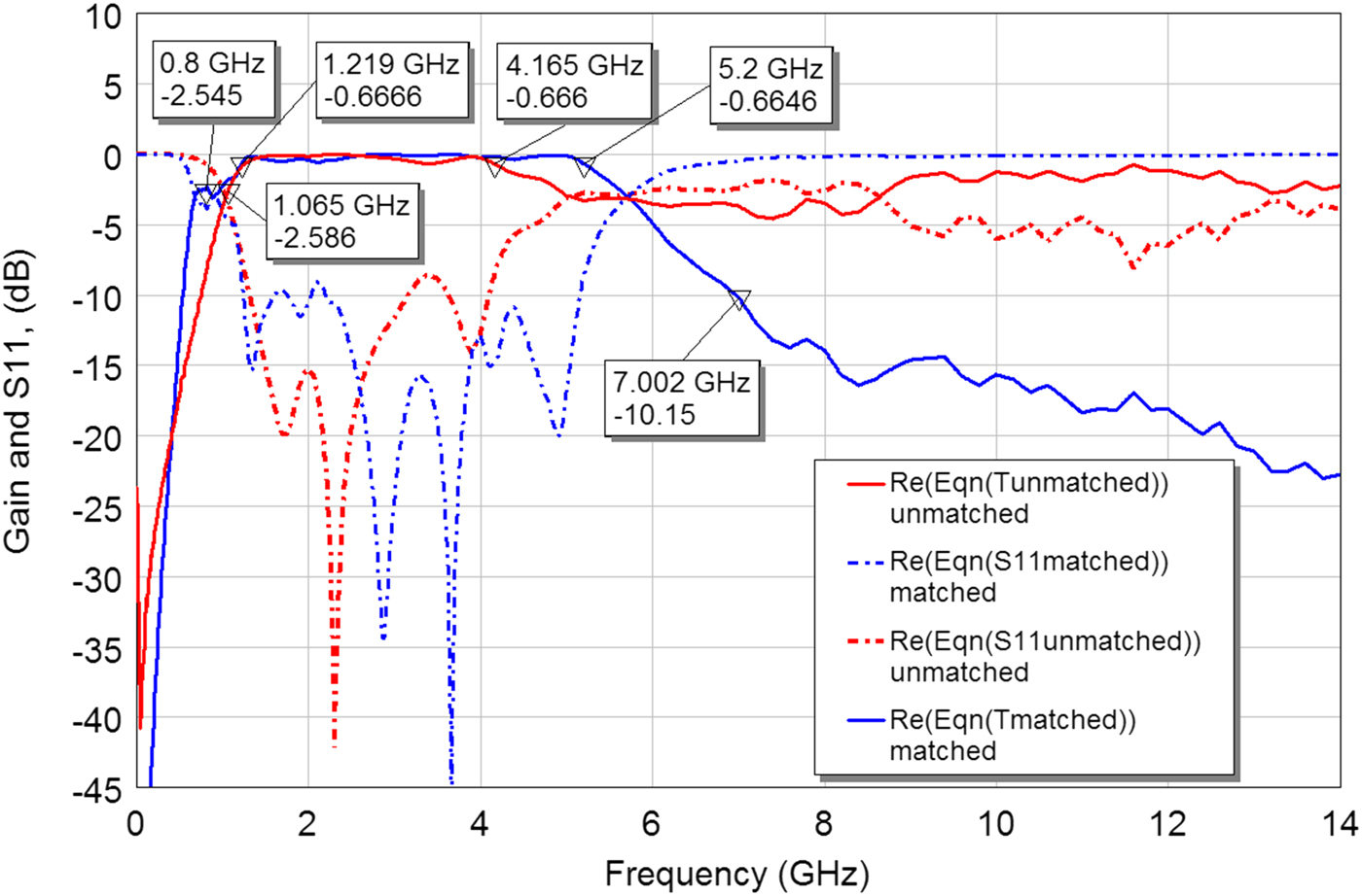
Designed BPMN matching network together with V-SPMA antenna seen in Fig. 3 is simulated in MWO [10] environment. Simulated gain curve of this BPMN–V-SPMA structure is seen in Fig. 4 in solid blue color. As understood from this curve, the new structure, i.e. the V-SPMA antenna equipped with the BPMN matching network, has the operating band ranging from 800 to 5200 MHz, a very wide frequency band in which many communication standards could be covered such as GSM, 3 G and Wi-Fi. Even though a large frequency band portion between 1.22–5.2 GHz has a very small gain deviation of ~0.66 dB, a relatively small frequency band between 800–1220 MHz has a large gain deviation of ~2.6 dB. This case is thought to be caused by the geometry of the antenna that is essentially designed for 2.4 GHz RFID applications and could be improved in a future work yielding a gain flatness alongside the whole 800–5200 MHz band.
MWO simulation setup for unmatched and matched antenna cases. (a) Unmatched antenna case: V-SPMA antenna without BPMN. (b) Matched antenna case: designed matching network (BPMN) together with V-SPMA antenna; BPMN–V-SPMA structure.

MWO simulation results: comparison of matched antenna gain (solid blue) and S 11 (dashed blue) to unmatched antenna gain (solid red) and S 11 (dashed red).
IV. DESIGN OF TRANSFORMERLESS MATCHING NETWORK VIA REOPTIMIZATION
Designed BPMN (of Fig. 3(b).) can be reoptimized to be able to obtain a new BPMN having 50 Ω resistive termination. To discriminate the BPMN of Fig. 3(b) from the newer reoptimized 50 Ω terminated version, we can name the former as BPMN_TR. Designed BPMN_TR has a transformer X 1 with a turn ratio of 1.464. It is a challenging engineering issue to construct an UWB “real-world” transformer that is to be able to operate alongside a very wide frequency band ranging from 0.8 to 5.2 GHz. Therefore, to avoid from the hard issues of constructing such a transformer, we should prefer to re-design a 50 Ω terminated (i.e. transformerless termination) BPMN, via a method that may be called as reoptimization.
When the analytic form of the normalized immitance (impedance Z(p) or admittance Y(p)) [Reference Yarman5], is synthesized as a lossless two-port in resistive termination, one may end up with a transformer depending on the value of the termination resistance. “transformerless” or 50 Ω terminated network is always desired in the final synthesis, however, this can be achieved for low-pass design problems only (see p. 361, [Reference Yarman5] and also [Reference Köprü, Kuntman and Yarman11]). Indeed, the back-end impedance of the designed BPMN_TR given by
 $${Z_B}\lpar p\rpar ={R_0}\displaystyle{{1+{\Gamma _B}\lpar p\rpar } \over {1 - {\Gamma _B}\lpar p\rpar }}={R_0}\displaystyle{{g\lpar p\rpar +h\lpar p\rpar } \over {g\lpar p\rpar - h\lpar p\rpar }}$$
becomes Z B (p = 0) = R 0(g n +1 + h n +1)/(g n +1 −h n +1) at DC, i.e. when p = jω = 0; where, the back-end reflectance is given as the ratio of “arbitrary” polynomial h(p) and “strictly Hurwitz” polynomial g(p) such that
 $${\Gamma _B}\lpar p\rpar =\displaystyle{{h\lpar p\rpar } \over {g\lpar p\rpar }}=\displaystyle{{{h_1}{p^n}+{h_2}{p^{n - 1}}+\cdots+{h_n}p+{h_{n+1}}} \over {{g_1}{p^n}+{g_2}{p^{n - 1}}+\cdots+{g_n}p+{g_{n+1}}}}.$$
By substituting hn+1 = 0, (10) results Z B (p = 0) = R 0 g n +1/g n +1 = R 0 = 50 Ω. This means that, for low-pass designs only, a matching network would have a 50 Ω standard termination resistance, i.e. a “transformerless” design [Reference Yarman5, Reference Köprü, Kuntman and Yarman11].
To the best of our knowledge, for bandpass design problems, it is a challenging task to obtain 50 Ω termination via a procedure similar to the method mentioned above for low-pass designs. On the other hand, reoptimization would not be so easy if the optimum topology of the designed BPMN_TR is not available. This is owed to the RFTs such as RFDCT and simplified real frequency technique (SRFT) [Reference Yarman5, Reference Yarman6, Reference Köprü, Kuntman and Yarman11] that helps one to determine the optimum topology (suited for the considered problem) of the non-50 Ω BPMN_TR as the initial design to be able to pass to the reoptimization stage if desired [Reference Köprü, Kuntman and Yarman11].
A) Reoptimization of BPMN_TR via simulation tool in MWO environment
Once the RFDCT determines the topology of the BPMN_TR as in Fig. 3(b), the reoptimization is performed via the simulation tool in MWO or ADS (Advanced System Design, Agilent Inc.) [10, 12].
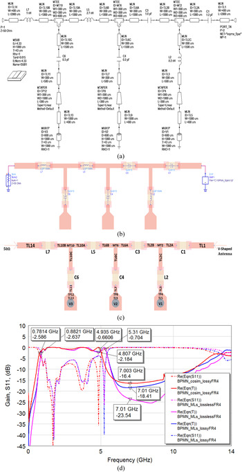
After removing the transformer X 1 from the BPMN_TR network seen in Fig. 3(b) and preserving its topology as the same and keeping the termination resistance (which is the resistance of Port 1) constant at 50 Ω, simulation tool in MWO environment can try to reach and track a preset gain curve trajectory of around 0 dB along the desired band of interest, i.e. from 0.8 to 5.2 GHz. Running this simulation tool optimizes the element values of BPMN_TR (Fig. 3(b)), i.e. ideal lumped component values (cval_ideal), ideal microstrip elements (mval_ideal) as microstrip lines MLINs, microstrip tee junctions MTEEs, microstrip tapered lines MTAPERs, and vias VIAs, in a such a way that the resulting gain curve (solid pink in Fig. 5(d) if the simulation runs with tanδ = 0 meaning that FR4 laminate is assumed as if it is lossless; or solid blue if the simulation runs with tanδ = 0.015 meaning that a lossy FR4 laminate is used) could track as much precise as the desired target gain curve (solid blue in Fig. 4) and, more importantly, not to cause the upper corner frequency to decrease much less than the desired value of 5.2 GHz. The values of ideal components and the dimensions of the ideal microstrip elements of the resulting optimized BPMN circuit schematics (shown in Fig. 5(a)) are given in Table 1. The material used in the MWO simulation is an FR4 laminate having the specs of dielectric constant ε r = 4.33, dielectric thickness h = 1 mm, copper thickness T = 43 µm, loss tangent tanδ = 0.015. Furthermore, by replacing the ideal lumped components of Fig. 5(a) with 402 case chip inductor and chip capacitor models from Murata LQP15MN and GJM15 series [13], a new schematics in the cosimulation tool of ADS as seen in Fig. 5(b) is formed. The pseudo-physical layout-like final pcb design is also seen in Fig. 5(c) drawn with 402 case lumped element footprints together with the routed microstrip element traces. Running the cosimulation with Fig. 5(b) schematics (with tanδ = 0.015), has resulted gain (solid red) and S 11 (dashed red) performances (seen in Fig. 5(d)) which are almost close to those (solid and dashed blue) of Fig. 5(a) (ideal) BPMN circuit.
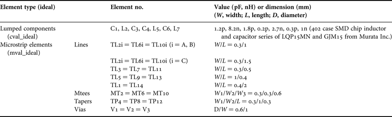
Comparison of BPMN with ideal elements and BPMN with Murata lumped component models. (a) MWO sim.: reoptimized BPMN with ideal lumped and microstrip elements. (b) ADS cosim. : BPMN with lumped component models from Murata. (c) ADS layout with lumped component footprints (402 case) and microstrip traces. (d) Comparison of gain and S11 performances: BPMN with ideal elements (with lossless and lossy FR4) versus BPMN with Murata lumped component models (with lossy FR4).

Values of ideal elements in BPMN in Fig. 5(a).
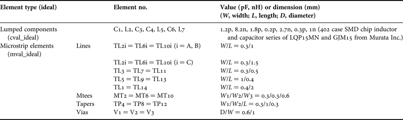
Note that the values of the lumped components used in the new reoptimized BPMN whose ideal, cosimulation and layout schematics are given in Figs 5(a), 5(b) and 5(c)), respectively, are standard values available in Murata 402 case chip inductor and capacitor series of LQP15MN and GJM15, respectively. Thus, we can produce the BPMN using Murata's standard microwave grade lumped components [13].
V. BPMN PRODUCTION AND ITS MEASUREMENT
The BPMN prototype board production effort consists of
-
• processing the layout pattern in Fig. 5(c) on a FR4 PCB laminate using a prototyping machine with model name “Elevenlab” from MITS Electronics Inc. [14] available in the circuit laboratory [15] of Istanbul University;
-
• soldering the Murata chip inductors and capacitors on the manufactured PCB; and
-
• soldering wires through the vias.
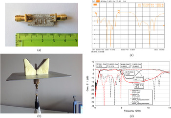
Resulting assembled board that measures 23 mm × 10 mm = 0.90 inch × 0.40 inch, ready for vector network analyzer (VNA: 10 MHz–14 GHz Rohde-Schwarz [16] available in the microwave and antennas laboratory [17]) measurements, is shown in Fig. 6(a). The SMA connector on the left edge of the board is connected to Port-1 of the VNA and the right edge connector is connected to the V-SPMA antenna's input port as seen in Fig. 6(b).
Prototype BPMN–V-SPMA setup and its VNA measurement results. (a) Assembled BPMN board ready for VNA measurements. (b) Final VNA measurement setup: BPMN board connected to V-SPMA antenna (BPMN–V-SPMA structure). (c) S 11 measurement result of BPMN–V-SPMA setup via VNA. (d) Gain and S11 performance comparison: BPMN_cosim versus BPMN–V-SPMA (measured via VNA).

Note that the gain performance (solid black in Fig. 6(d)) of the BPMN–V-SPMA setup is computed via an MWO equation that uses the s1p touchstone file belonging to the measured S 11 data (Fig. 6(c)) such that
 $$\eqalignno{ T\lpar {\omega _i}\rpar &=1 - {\left\vert {{S_{11}}\lpar {\omega _i}\rpar } \right\vert ^2}\comma \; {\omega _b} \leq {\omega _i} \leq {\omega _e}\comma \; \cr i&=\lcub 1\comma \; 2\comma \; ...\comma \; nd\rcub \comma \;} $$
where ω i is the ith frequency at which the gain T(ω i ) is evaluated. nd is the number of data uniformly distributed in the frequency axis ranging from f b = 100 MHz to f e = 14 GHz, where f b and f e are the start and the stop frequencies, respectively, in the measurement range of VNA.
VI. CONCLUSIONS
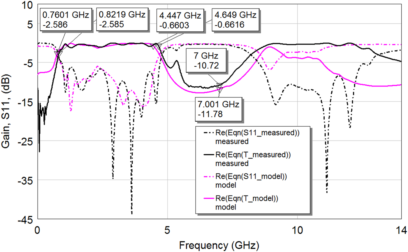
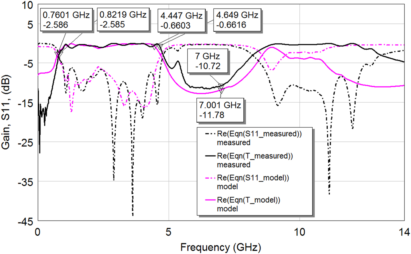
V-SPMA antenna equipped with the designed matching network (BPMN) achieves a good passband gain performance in a wide (0.8223–4.666 GHz) frequency range as seen in Fig. 6(d) (solid black) if the upper corner frequency is considered at −0.6602 dB point. If −3 dB point is considered, the upper corner frequency can be thought as 4.79 GHz. Gain deviation does not exceed the value of −1.2 dB along the passband from 1.3 to 4.666 GHz, whereas the stopband attenuation is −10.77 dB at about 7 GHz. This is 12.77 dB higher than that of the ideal circuit (Fig. 5(a)) whose stopband attenuation is −23.54 dB as seen in Fig. 5(d) (solid pink), obtained via simulation of Fig. 5(a) with an FR4 which is assumed as if it is a lossless laminate, i.e. tanδ = 0.
The amount of the attenuation can be estimated with
 $\alpha=2.3f\tan \delta \sqrt {{\varepsilon _{eff}}} $
[Reference Leys18], where α is attenuation in dB/inch, f is the operating frequency in GHz, tanδ is the material dissipation factor or loss tangent, ε
eff
is the effective relative dielectric constant of the material [Reference Leys18]. Thus, the attenuation of a 7 GHz signal traveling over the BPMN board seen in Fig. 6(a), which measures 0.9 inch in length, would be
 $\alpha=\left({2.3\lpar 7\rpar \lpar 0.015\rpar \sqrt {4.33} \, {\rm dB}/{\rm inch}} \right)\times 0.9\, {\rm inch}=0.45\, {\rm dB}$
. Although the microwave grade laminates are suggested to be used at very high frequencies [Reference Leys18] instead of FR4, the prototyping machine [14] in our lab [15] has not the capability to process laminates such as RT5880 [19] (Rogers corp.). On the other hand, such a high attenuation of 12.77 dB mentioned above cannot be attributed to the calculated attenuation factor α of only 0.45 dB aroused due to use of FR4.
A) Proposed lossy BPMN model
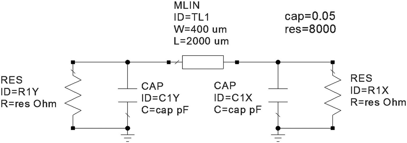
The underlying reason that causes the measured BPMN gain (solid black in Fig. 6(d)) at stopband cannot be lowered below −10.77 dB (at 7 GHz) is thought to be the large number of distributed leakage capacitors and conductances (equivalently resistors), between each microstrip lines and ground plane, in the ideal BPMN circuit of Fig. 5(a) (with lossless FR4, i.e. tanδ = 0). An equivalent microstrip line model, having distributed leakage capacitors and conductances, that may help to mimic each microstrip line used in prototype BPMN, could be proposed as seen in Fig. 7.
Proposed lossy microstrip line equivalent model that may mimic each microstrip line used in the prototype BPMN.

Replacing each of the microstrip lines in Fig. 5(a) by the microstrip line model proposed in Fig. 7, yields a new real-like BPMN model, having a total of 34 such distributed leakage capacitors and 34 conductances that might allow us to estimate not only the passband but also the stopband performance. Leakage capacitances and conductances of the model are estimated roughly by trial and error as 50 fF and 125
 $\mu \mho $
. Fig. 8 shows how the ideal BPMN (Fig. 5(a) with tanδ = 0), formed with such microstrip line models of Fig. 7, estimates the stopband attenuation performance (solid pink) closely to that of the measured BPMN (solid black in Figs 6(d) and 8). Unsuccessful representation of the measured gain curve beyond about 8 GHz by the proposed model might be enhanced by inserting new reactive elements into the proposed model in a dedicated work in the future.
Gain and S11 performance of BPMNs: prototype (measured) BPMN versus BPMN with proposed lossy microstrip line model.
With the aid of the RFDCT matching network design technique, a single V-SPMA antenna, essentially designed for 2.4 GHz RFID applications, has been made a convenient structure that could sufficiently meet applications employing with many communication standards ranging in the 800–5200 MHz frequency band. Full-band (0.8–5.2 GHz) gain flatness could be achieved once a new V-SPMA antenna built and equipped by a new BPMN matching network in a future work. We may forecast that stopband performance might probably further be enhanced by lowering the attenuation as much as possible. To achieve this, i.e. to obtain sharp gain roll-off at high frequencies to lower the stopband attenuation further, to the best of our knowledge, the designer should increase the number of elements in the topology of the matching network, seen in Fig. 3(b), if she/he prefers to use Butterworth or Chebyshev-type target gain function in the optimization. However, this might cause much more complex matching networks. Another approach can be the use of ladder-type elliptical bandpass matching network design that is essentially have finite transmission zeros that highly sharpens the gain roll-off with reasonably low number of elements compared to the Butterworth/Chebyshev fashion design [Reference Yarman5, Reference Wilamowski and Gottiparthy20]. All-microstrip element approach can also be adopted in a future work to avoid from the use of all-lumped element approach utilized in the paper. In that context, the Matlab code have to be converted from Laplace domain (p = jω; Laplace variable) to Richards domain (λ = jtan(ωτ); Richards variable) [Reference Yarman5] (τ is the delay length of the microstrip UEs – unit elements – in seconds) in which the synthesis technique must also be switched from high-precision lumped synthesis package [Reference Kılınç and Yarman21, Reference Yarman and Kılınç22] to high-precision Richards synthesis package [Reference Yarman, Köprü, Kumar and Prakash23] which yields UEs (commensurate lines, i.e. equal length transmission lines) as circuit elements [Reference Yarman5, Reference Yarman, Köprü, Kumar and Prakash23].
While the RFTs are very well-known and commonly used numerical design techniques frequently encountered in the literature to design wideband matching networks, filters and microwave amplifiers, the work in this paper, to the best of our knowledge, presents the utilization of RFT in a new application, which is an UWB V-SPMA matching network design to create a one-single UWB multi-standard antenna environment which can cover many communication standards such as cellular phone systems (900 MHz and 1800/1900 MHz) as well as 3 G (2.1–2.6 GHz) and Wi-Fi (2.4 and 5.2 GHz) frequency bands. Such a single V-SPMA in a wireless system could decrease the problems arising from system complexities due switchings, high costs, high circuitry areas, high DC power consumption caused by many separate dedicated narrow-band antennas, and its accompanying matching elements.
When the V-SPMA antenna is equipped with a standard 50 Ω wideband bandpass matching network, one can easily utilize this BPMN–V-SPMA structure by directly connecting to the 50 Ω compatible output of a commercially available wideband power amplifier (PA) (such as [24] from minicircuits inc. [25]) avoiding the very challenging design issues of an interstage network between the output of the PA and the V-SPMA antenna. This way, challenging matching network design issue turns into an easy cascading of commercially available 50 Ω output PA [24] and such a matched-antenna structure presented in the paper.
ACKNOWLEDGEMENT
The work reported here was carried out at Işık University and Istanbul University. It is funded by Scientific Research Projects Coordination Unit (BAP) of Istanbul University under the project code 18549. We here thank to Dr. Koray Gürkan, of Istanbul University, for his invaluable contributions in pcb board manufacturing via prototyping machine.
 Ramazan Köprü received his B.Sc. from Yıldız Technical University, M.Sc. and Ph.D. degrees from Istanbul Technical University in 1991, 1994 and 2013, respectively, all in Electronics and Communications Engineering. In the past, he has worked as electronics design engineer in R&D departments of private sector in the fields of embedded systems, wireless systems, power electronics and defense electronics. His main interest areas of research are military spec low noise wideband analog design for laser signal detection and postprocessing, wideband microwave power amplifier design using real frequency techniques, network synthesis with lumped and distributed elements, non-linear wideband microwave amplifier design using X-parameters, wideband filter and matching network design using search and particle-swarm optimizations, lumped and distributed matching network design for microstrip patch antenna for UWB applications. He is currently work as Assistant Professor in Electrical-Electronics engineering department of Işık University, Turkey.
 Sedat Kilinç received his B.Sc. degree in Electronics and Communications Engineering from Yildiz Technical University in 2012 and is currently studying toward his M.Sc. degree in Istanbul Technical University. He has been a Research Assistant in Istanbul University since 2012. His interest areas are microwave and RF circuits, non-linear microwave power amplifier design, and wideband microwave power transfer network synthesis with lumped and distributed elements.
 Çağatay Aydin received his B.Sc. degree in Physics and M.Sc. degree in Electrical and Electronic Engineering from Istanbul University, Turkey, in 2008 and 2011, respectively, and is currently working toward the Ph.D. degree at Electrical and Electronics Engineering of Istanbul University. Since 2008, he has been a teaching assistant in Istanbul University and also he has been employed as an instructor at Işık University since 2012.
 Doğu Çağdaş Atilla received his B.Sc. degree in Physics and M.Sc. degree in Electrical and Electronics Engineering from Istanbul University in 2008 and 2011, respectively. Currently, he is pursuing his Ph.D. degree at Electrical and Electronics Engineering of Istanbul University. His main fields of interest are wideband antenna design, tunable amplifiers, and RF hardware. Currently, he has been employed as an instructor at Işık University since 2012.
 Cahit Karakuş received his B.Sc. and M.Sc. degrees in Electronic and Communication Engineering from Istanbul Technical University, Turkey, in 1984 and 1987, respectively. He received Ph.D. degree from the Institute of Science, Istanbul Technical University, Turkey. He has also experience in antenna technologies. He has been working as a specialist in the defense industry since 2007.
 Binboğa Siddik Yarman received his B.Sc. degree in Electrical Engineering from Istanbul Technical University (1974), M.Sc. from Stevens Institute of Technology, NJ, USA (1978), and Ph.D. from Cornell University, Ithaca, NY, USA (1982), respectively. He had been a member of technical staff at David Sarnoff Research Center where he was in charge of designing satellite transponders for commercial and military agencies in the USA. He returned to Turkey in 1984 and served as assistant, associate, and full professor at Anatolia University-Eskişehir, Middle East Technical University-Ankara, Istanbul Technical University, and Istanbul University, Istanbul, respectively. He had been the chairperson of Department of Electronics Engineering, Defense Technologies and Director of School of Technical Sciences of Istanbul University over the years 1990–1996. He was the founding president of Isik University. He had been a visiting professor at Ruhr University, Bochum (1987–1994) and Tokyo Institute of Technology (2006–2008). Currently, he is the Chairman of Department of Electrical-Electronics Engineering in Istanbul University.