Introduction
Biomimetic patterns serve as an inspiration for designing materials with various optical properties, from iridescence to transparency. In an age of screens, displays, and optoelectronic devices, there is an enduring interest in eliminating reflectivity from surfaces. Traditionally, this result has been achieved by applying layered antireflective coatings (ARCs) so that the scattering of light in the direction of its source is inhibited by destructive interference at the layer interfaces.[Reference Macleod1] It is difficult to achieve broadband and omnidirectional antireflection with this approach, because it can only reduce reflection at a few wavelengths and at specific incident angles.[Reference Cai and Qi2] Inspiration for improving ARCs and arrays can be drawn from examples of non-reflectivity and transparency observed in nature, which are often a result of nanoscale structures. Recent work on the glasswing butterfly has shown that broadband, omnidirectional anti-reflective properties can be achieved by randomly sized nanopillars with a characteristic length scale below the wavelength of light.[Reference Siddique, Gomard and Holscher3] We demonstrate how such structures can be replicated directly on a glass substrate, leading to a significant decrease in the reflection of incident light.
Conventional ARCs involve coating the reflective surface with a thin multilayer film where the refractive indices and film thicknesses are selected such that the reflections of light occurring at each of the film's interfaces destructively interfere with each other.[Reference Hecht4] However, there are a number of shortcomings such as poor mechanical durability, sensitivity to thickness variations, and performance limited to a narrow range of incident wavelengths and angles.[Reference Guenther5] An alternative strategy to achieve non-reflectivity is to eliminate the sharp change in refractive index at the surface by gradually changing the refractive index from one refractive index to another.[Reference Raut, Ganesh, Nair and Ramakrishna6] From a technologic standpoint, this phenomenon can be achieved by varying the packing density (i.e., porosity) throughout the thickness of the film or coating and by ensuring that the pores are smaller than the wavelength of light.[Reference Yoldas7] However, these changes in film density typically come at the cost of the film's mechanical properties and consequently raise questions regarding their robustness.
Studies of night-flying moths in the 1960s revealed that the corneal lens of these insects is covered by a hexagonal array of sub-wavelength structures (SWSs),[Reference Bernhard, Miller and Moller8] which reduces the reflection of light and ensures that the moth remains camouflaged from predators.[Reference Clapham and Hutley9] Such structures have since been observed in the transparent wings of hawkmoths and cicadas.[Reference Yoshida, Motoyama, Kosaku and Miyamoto10,Reference Morikawa, Ryu, Seniutunas, Balcytis, Maximova, Wang, Zamengo, Ivanova and Juodkazis11] Studies on SWSs with dimensions smaller than the wavelength of light reveal that these surfaces can be treated as a thin film with a spatially varying effective refractive index, which gives rise to antireflective properties.[Reference Craighead, Howard, Sweeney and Tennant12] Unlike conventional ARCs, the antireflective properties of SWSs are broadband and omnidirectional.[Reference Halir, Bock, Cheben, Ortega-Monux, Alonso-Ramos, Schmid, Lapointe, Xu, Wanguemert-Perez, Molina-Fernandez and Janz13] Many approaches have been used to replicate these structures synthetically in silicon,[Reference Siddique, Donie, Gomard, Yalamanchili, Merdzhanova, Lemmer and Hölscher14–Reference Chan, DeCuir, Fu, Morse and Gordon16] zinc chalcogenides,[Reference Huang, Jen, Chen, Chen and Chattopadhyay17] and organic materials.[Reference Chen, Huang and Yang18] Cicada wing-inspired structures have been successfully imitated on polymer substrates,[Reference Zhang, Zhang, Xie, Liu and Shao19] and cicada wings themselves have been used as a bio-template to replicate the wing surface structure on polymethyl methacrylate substrates.[Reference Xie, Zhang, Lin, Zhang, Liu and Mu20] Moth-eye-like structures have been replicated with nanoimprint lithography on transparent polycarbonate substrates.[Reference Sun, Wang, Wu, Jiang, Shen, Cooper, Zheng, Liu, Yang and Wu21]
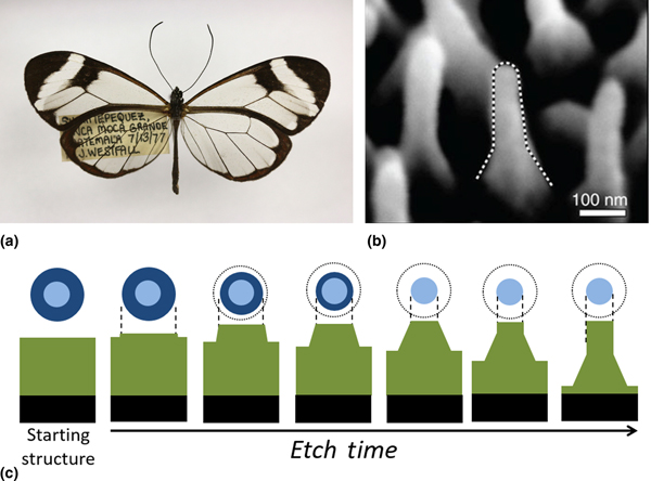
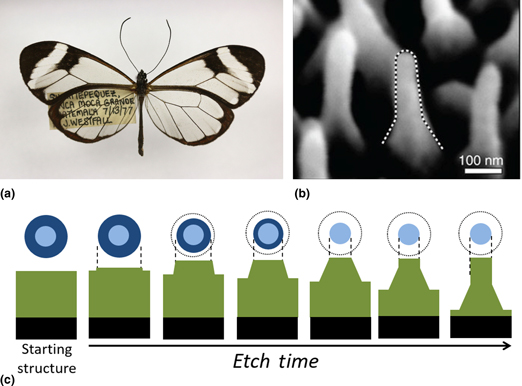
The transparent wings of the glasswing butterfly (Greta oto) [Fig. 1(a)] have remarkable optical properties, notably anti-reflection at large viewing angles and across a broad spectrum of wavelengths. While at first it was suggested that these optical properties result from the same mechanism that is found in moth eyes,[Reference Binetti, Schiffman, Leaffer, Spanier and Schauer22] Siddique et al. demonstrated that it is actually due to the high degree of randomness in the size and spatial distribution of uniquely shaped nanopillars [Fig. 1(b)].[Reference Siddique, Gomard and Holscher3] Additionally, these nanopillars feature much higher aspect ratios (up to ten), while all nipple structures use aspect ratios of one to two. The glasswing structural pattern has been thoroughly imaged and the interaction of light with these nanostructures has been simulated, but it had yet to be reproduced synthetically. In this paper, we replicate these structures and demonstrate their effectiveness in decreasing the surface reflectivity on a glass substrate.
(a) Glasswing butterfly (Greta oto). Credit: Andrei Sourakov. (b) Scanning electron micrograph (SEM) shows the random nanopillars on a glasswing butterfly wing. Reproduced with permission from Ref. [Reference Siddique, Gomard and Holscher3] 2015, Springer Nature. (c) Process used to replicate glasswing nanostructures in silica. Reactive-ion etching of oxidized silver dewetted islands allows us to achieve a nanopillar structure with a wider, cone-shaped base. Green represents the sputtered silica layer, light blue represents silver metal, and dark blue represents silver oxide.

The design specifications for these nanostructures were based on the following characteristics, reported by Siddique et al.[Reference Siddique, Gomard and Holscher3] The average characteristic distance between pillars is 100–140 nm (lower than the wavelengths considered). The typical aspect ratio of the nanopillars is five (with some achieving a ratio of ten); the height and radius of the pillars are 400–600 and 40–60 nm, respectively. The pillars are situated atop cone-shaped pedestals with a typical height of 160–200 nm. The heights of the pillar and average distance between them follow a Gaussian distribution with a variance of 100 and ~120 nm, respectively.
We applied directional etching to a dewetted silver thin film that had been deposited upon a pure silica substrate. The silver thin film dewetted into non-uniform droplets that mimicked the random spatial distribution of the nanopillars on the wings of G. oto. The expansion of silver upon oxidation allowed us to create nanopillars with a wider, tapered base, which, in simulations, was shown to be the ideal shape for maximizing anti-reflection. Figure 1(c) illustrates the directional etching approach we used. Upon removal of the silver mask, we were left with a transparent silica substrate with significantly lower reflectance.
Materials and methods
Materials selection
In choosing a material to be etched, we considered two criteria: (1) the resulting film would have to have the right optical properties, and (2) the material would have to be compatible with directional etch chemistry. Hence, we looked for a robust material that is inert in its solid state with low absorption in the visible wavelengths and that could be formed into a thin film. Ideally, the etch by-products of the chosen material would volatilize upon being etched with conventional reactive-ion etching (RIE) technology. After considering several materials (Table SI), we chose silica as it met the above criteria best. Silica can be deposited by sputtering, chemical vapor deposition, or obtained as-is, and it is easily etched.
Solid thin films are usually metastable or unstable as-deposited and will aggregate to form pools of material, or islands, when heated to sufficiently high temperatures.[Reference Thompson23] This kind of dewetting is strongly dependent on material, temperature, and film thickness. Our target material was one that would dewet in air and expand when oxidized. Table SII summarizes our considerations and the basis of our selection of silver as the thin film to dewet. We chose silver because it dewets above 200 °C in air (rather than oxidizing in these conditions, as tin and copper do) and expands significantly when oxidized.
Etch mask formation
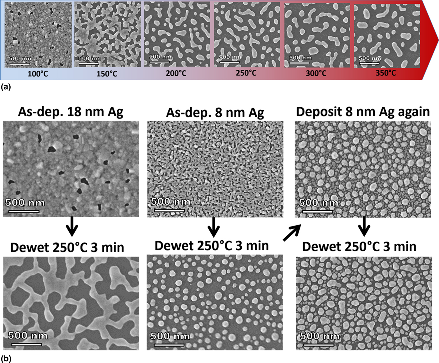
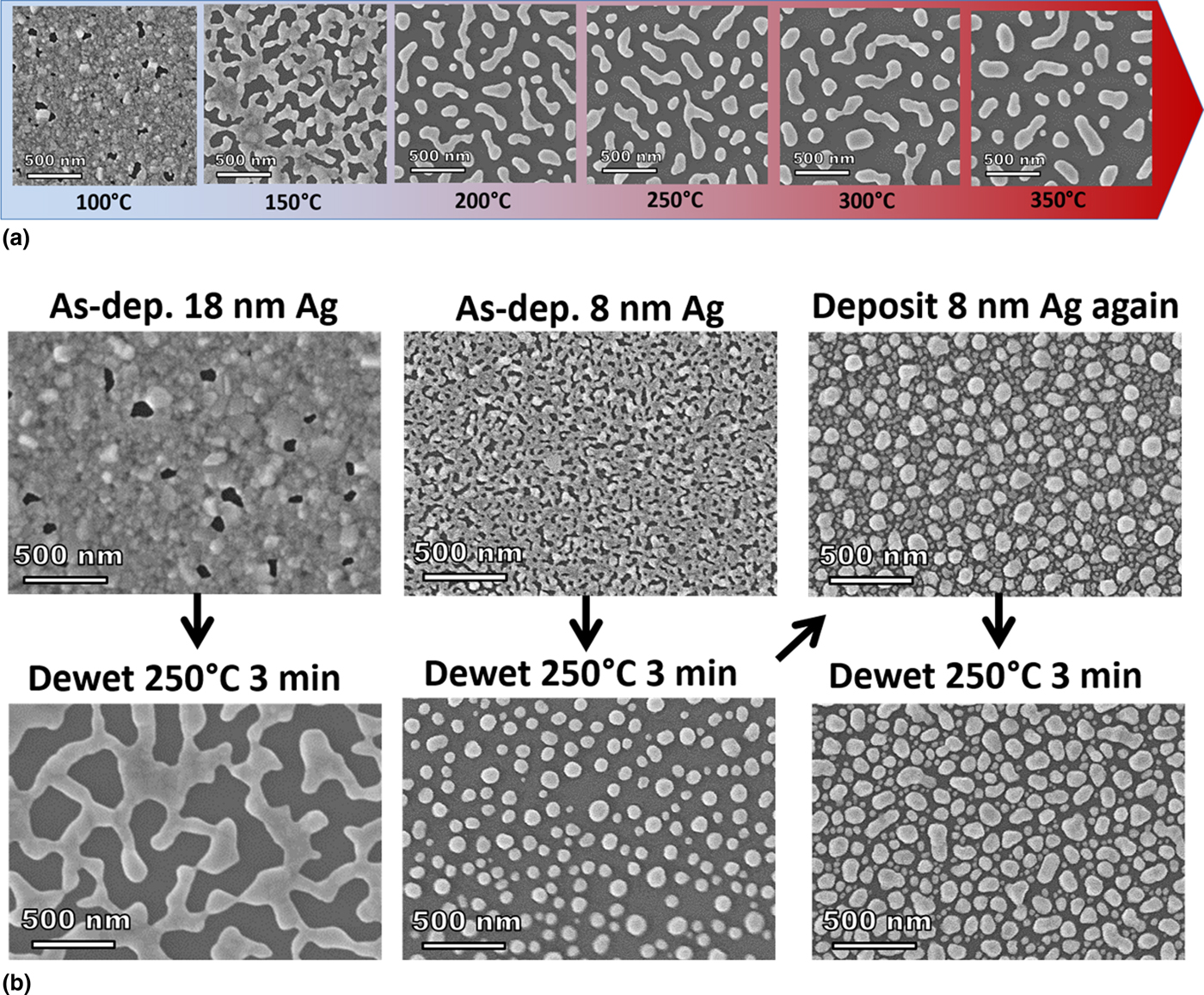
The etch mask was formed by first spin-coating a metal thin film. Thin films with thicknesses of 8, 14, and 18 nm were tested. Using a hot plate for dewetting, we observed changes in film morphology as a function of temperature. We dewetted a 14 nm Ag thin film for 1 min at temperatures ranging from 100 to 350 °C, at increments of 50 °C [Fig. 2(a)]. Once we determined the temperature that produced the optimal surface morphology for the etch mask, these conditions were used for further investigations on the effect of material and thin film thickness on the resulting etch mask pattern. Silver thin films of 8 and 18 nm thickness were dewetted at 250 °C for 3 min [Fig. 2(b)]. We found that dewetting a silver film and then re-depositing an 8 nm layer of silver, which was then dewetted again using the same conditions, resulted in an even larger range of droplet sizes, which was ideal for our purposes. To achieve the desired tapered pillar structure, dewetted silver films were oxidized prior to etching by heating the samples on a hotplate in air at 250 °C. Varying the duration of heating and the temperature affected the degree of oxidation and thus the particle size.
(a) Dewetting morphology of Ag thin film as a function of temperature (1 min, 14 nm Ag film). (b) Scanning electron microscope images demonstrating dewetting morphology as a function of material and thin film thickness.
Reactive-ion etching
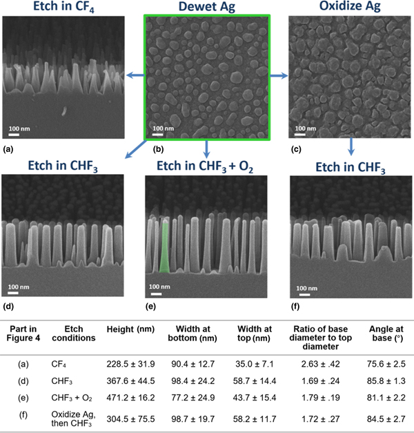
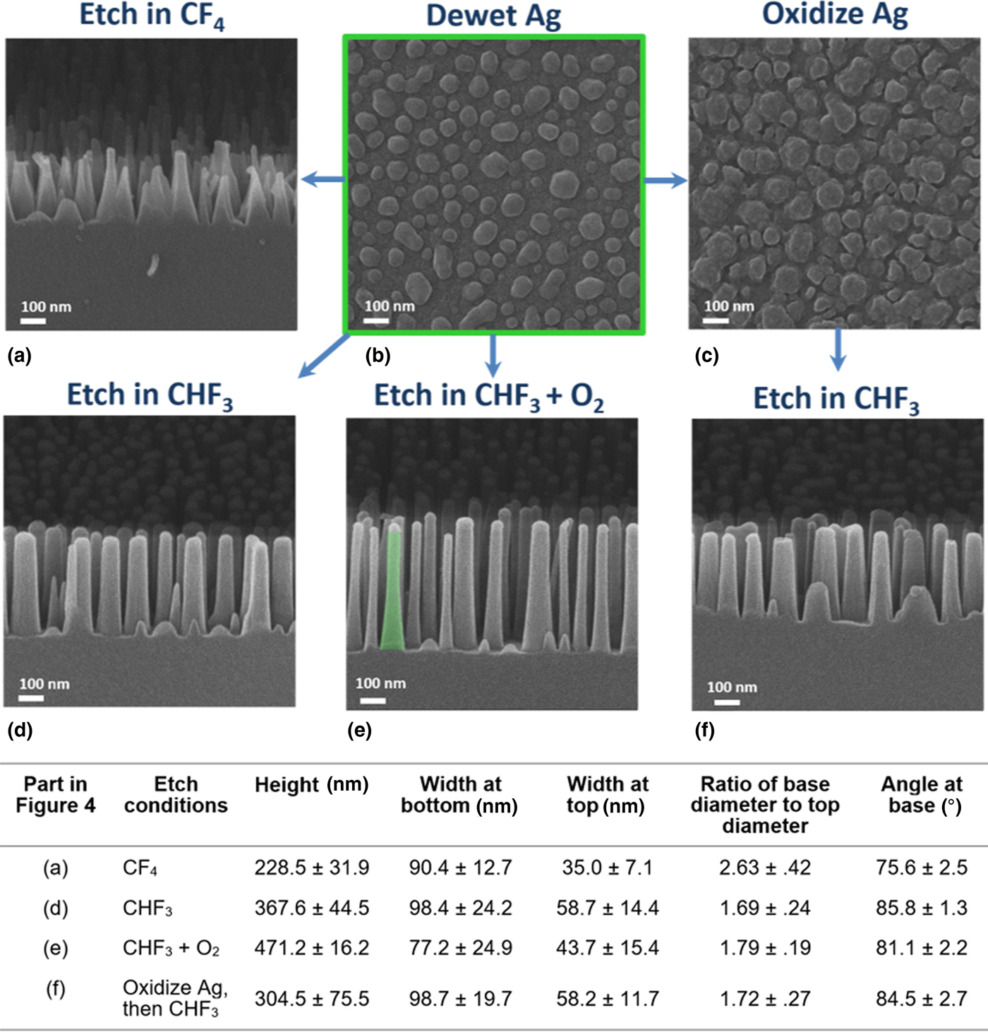
Etch masks that were formed using the double dewetting of an 8 nm silver thin film were etched under various conditions using a Plasmatherm reactive ion etcher to perform dry etching. Directional etching with CF4 and CHF3 (5 min, 10 mT, 150 W) showed that CHF3 resulted in nanopillars with high aspect ratios. In order to achieve a tapered base in the nanopillar structure, oxygen gas was added to the flow of CHF3. The outer surface of the silver droplets was oxidized, which caused droplets to expand in size due to the lower density of silver oxide as compared to silver. When the sample was then etched after oxidation, the silica substrate was etched away rapidly, while the silver oxide was etched at a slower rate. The remaining silver mask was removed post-etching by wet etching the silver and then rinsing with deionized water. Nanopillar size statistics (height, width at top and bottom of pillars, angle between substrate and base of pillar, aspect ratio) were quantified with ImageJ software.
Results and discussion
In order to consistently achieve the desired results from the dewetting process, it was necessary to first understand the dewetting properties of the thin films under consideration. The initial thin film thickness, the dewetting temperature, the duration of the dewetting, and the composition of the thin film all determined the surface morphology of the dewetted film. Higher dewetting temperatures resulted in larger spacing between droplets [Fig. 2(a)]. Thicker thin films (18 nm) formed a contiguous, mosaic-like pattern, while the thinner films (8 nm) formed spherical, isolated droplets [Fig. 2(b)]. The latter, 8 nm Ag thin films dewetted at 250 °C for 3 min, resulted in droplets with the desired size and shape to be used as a template for etching cylindrical nanopillars, but the spacing between them was too large. This was resolved by dewetting one such thin film, and then depositing another 8 nm Ag thin film and dewetting under the same conditions. Not only did this increase the density of Ag droplets on the surface, but it also gave us an even greater distribution of droplet size. In Siddique et al.'s simulation, a random distribution of nanopillar diameter and height was shown to be ideal to minimize the amount of light that was scattered in the direction of the source.
Directional etching of the dewetted silver mask using CHF3 and CF4 revealed a high selectivity between Ag and SiO2 (Fig. 3). We were able to achieve aspect ratios of up to 20 for 20 min-long etches using CHF3. As expected, the silver particles expanded in size when they were oxidized, which allowed us to obtain a tapered base on the nanopillar when the silver mask was etched in the presence of oxygen. We were able to meet our design specifications of approximately randomly distributed nanopillars of varying diameters and heights in the range of about 40–100 and 200–500 nm, respectively, with a tapered base. The size statistics for the nanostructures are presented in the table in Fig. 3. Etching with CF4 resulted in short pillars with a wide base and a large cone-shaped pedestal. Substrates that were etched with CHF3 only and those that were first oxidized and then etched with CHF3 produced similarly shaped pillars with aspect ratios of about five but without much of an inclined base. When oxygen was used in tandem with CHF3 for RIE, higher aspect ratios were achieved along with more pronounced (more angled) pedestals.
The starting template for all experiments with directional etching was the silver thin film after dewetting (b). Different etching conditions yielded a variety of nanostructures: using CF4 gas (a) versus CHF3 (d), oxidizing prior to etching (f), or etching in the presence of oxygen (e). The expansion of the silver particles upon oxidation can be seen clearly by comparing (b) and (c). The table in this figure presents dimensional statistics for the nanostructures obtained using each of the above etch conditions.
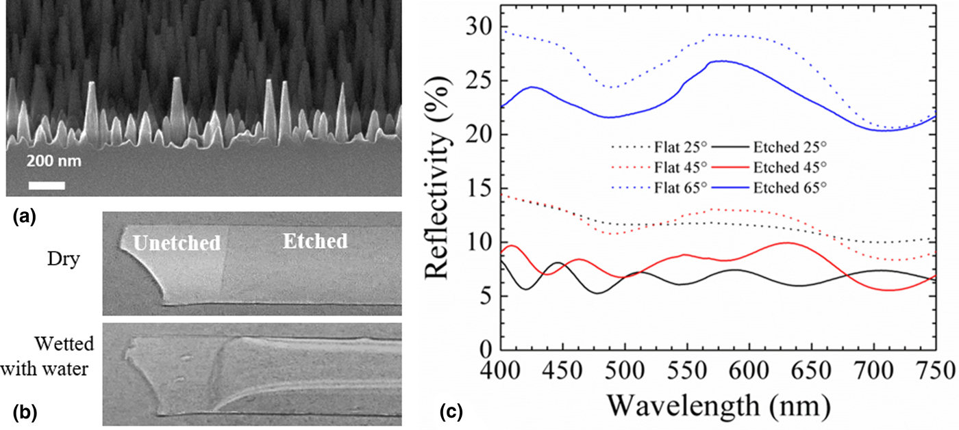
Removal of the silver mask damaged some of the nanopillars [Fig. 4(a)], but enough of the nanostructure array remained to significantly reduce reflectivity. These nanopillars have an average height of 213.0 ± 91.4 nm, an average base width of 68.2 ± 13.2 nm, and an average base angle of 79.8° ± 6.2°. The structures are more cone-shaped than those shown in Fig. 3 and most taper to a point at the top (average width at the top is therefore not quantified). The average aspect ratio (defined here as height divided by the width halfway up the pillar) is about six for this nanostructure array.
(a) Nanopillars after the silver mask was removed. (b) Photograph of a sample. Half of the sample in the photo has been etched, while the other half remains untreated, allowing for a qualitative contrast between the two surfaces. The lower photograph demonstrates the etched surface's hydrophobic properties. (c) Percent of incident light reflected as a function of wavelength. Comparison of etched versus non-etched samples for three viewing angles. For each viewing angle and across most of the spectrum from 400 to 700 nm, the etched sample reflected 2–8% less visible light than the non-etched sample.
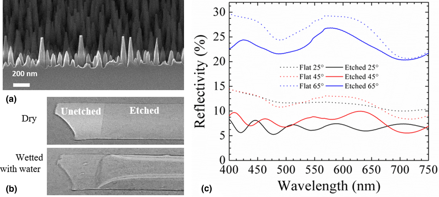
The results of reflection spectroscopy performed on etched and unetched samples for three different viewing angles (25°, 45°, 65°) are plotted in Fig. 4(c). For untreated substrates, the percent reflectivity of incident light ranged from about 5% to 9% and 5% to 10% across the visible spectrum for viewing angles of 25° and 45°, respectively. Single-sided nanostructuring of a glass substrate improved transmission by 2–6% for light between 400 and 750 nm for these viewing angles. The reflectivity was much higher for a viewing angle of 65°, in the range of 20–30%. Single-sided etching reduced reflectivity by as much as 8% (for 400 nm light), with the effect tapering off as the wavelength of incident light approached 700 nm. An additional result of the surface modification was that water does not readily wet the surface due to an increased surface roughness [Fig. 4(b)].
Because the dimensions of the structures are less than the wavelength of light and the same “dimensional constraints are applied to the spacing and depth between nanostructures […], light rays get trapped in the crevices resulting in multiple internal reflections.”[Reference Raut, Ganesh, Nair and Ramakrishna6,Reference Craighead, Howard, Sweeney and Tennant24] The non-uniform size and spacing reduce the probability that any of the light trapped in these “crevices” will interfere coherently. While it is likely that higher aspect ratios augment the trapping effect and allow even less light to scatter in the direction of the source, there is the concomitant effect that nanopillars with higher aspect ratios are mechanically less robust. This issue of robustness can be addressed by compromising with smaller aspect ratios or experimenting with stress engineering (e.g., tempered glass).
When deciding which fabrication method would be most suitable, we first considered top-down approaches, such as nanoimprint lithography or hot embossing, which were tentatively suggested in Siddique et al.[Reference Siddique, Gomard and Holscher3] However, techniques that require a master mold or stamp not only would have been more expensive, but they may not have yielded as random a distribution in the size and spacing of the nanostructures as outlined in the design specifications. The mask-and-etch approach that we selected proved to be ideal because it can be done quickly (etches took ~20 min) and without waste of materials, as the silver thin film used as the mask can be recovered once it has been removed from the substrate. Additionally, the methods used in the present study can easily be scaled up, as numerous systems exist for silver and oxide deposition and RIE can be applied to large surface areas. Such considerations will be important for integrating this surface modification technique into existing optoelectronic technologies and other large-area applications.
Cost is a major concern for the industry, particularly for large-area applications. Studies have shown that ARCs can provide positive net present value in greenhouses or photovoltaics if their added cost can be <$7.5/m2 or <$14/m2, respectively.[Reference Jorgensen, Brunold, Koehl, Nostell, Oversloot, Roos, Lampert and Granqvist25] A back-of-the-envelope cost analysis for our technique indicates that it can be implemented at a cost on the order of $0.50/m2. Assuming that silver costs $485/kg,[Reference Gil-Alana, Aye and Gupta26] and we use a 10 nm Ag thin film (3 min) per square meter, the cost is ~5¢. Large-scale plasma-enhanced chemical vapor deposition costs $1.5 × 10⁻⁴/m2 and 1 µm of SiO2 (15 min) costs 15¢.[Reference Madocks, Seaman and McClure27] To dewet the Ag film using a hot plate run at 200 °C (5 min) in air assumes a cost of 20¢, with comparable scaling if oven racks were used. The total time to pattern 1 m2 would be about 1 h.
Conclusion
By tuning the thickness of the metal thin film and the etching and dewetting duration, we were able to emulate the characteristic nanostructures observed on the wings of the glasswing butterfly. Through reflection spectroscopy, we showed that performing this surface modification decreased reflection by 2–8% for large viewing angles, which is a significant amount in a field where progress is often measured by tenths of a percent. A National Renewable Energy Laboratory (NREL) report on ARCs for photovoltaics estimated that a 5% increase in solar transmittance could result in as much as a 10% improvement in energy collection efficiency.[Reference Jorgensen, Brunold, Koehl, Nostell, Oversloot, Roos, Lampert and Granqvist25] With growing interest in multifunctional coatings, it is noteworthy that the nanostructure array that we fabricated also has hydrophobic and anti-fogging properties. Having a built-in ability to repel water, dust, and contaminants is an advantage for the production of transparent materials. The next steps in the wake of this proof-of-concept are improving the robustness and durability of these nanopillars, scaling up to a larger surface area, and testing the process on polymer films with high glass transition temperatures.
Supplementary material
The supplementary material for this article can be found at https://doi.org/10.1557/mrc.2019.57
Acknowledgments
The early stage of this work was supported by the National Research Foundation of Singapore through the Singapore-MIT Alliance for Research and Technology's Low Energy Electronic System interdisciplinary research group. The opportunity for this research was provided by Materials Solutions for Sustainability (MADMEC) at the Massachusetts Institute of Technology. MADMEC is supported by the MIT Department of Materials Science and Engineering, Dow Chemical, and Saint-Gobain. We would like to thank Dr. Michael Tarkanian and Professor Carl Thompson for their feedback on experimental design. We are grateful to Dr. Michael Christiansen and Dr. Andrei Sourakov for reviewing the manuscript and providing useful suggestions.
Figure 1b reprinted with permission from [Springer Nature Customer Service Centre GmbH]: [Springer Nature] [NATURE COMMUNICATIONS] [R. H. Siddique, G. Gomard, H. Hölscher, Nat. Commun. 6, 6909 (2015). (The role of random nanostructures for the omnidirectional anti-reflection properties of the glasswing butterfly, Radwanul Hasan Siddique, Guillaume Gomard, Hendrik Hölscher), [COPYRIGHT 2015].