I. INTRODUCTION
Cost reduction, device functionality, and energy efficiency are the major driving forces in semiconductor and microelectromechanical system miniaturization. Over the years, progress in miniaturization and the appearance of new functional materials has led device feature sizes to venture into the nanometer size regime.Reference Craighead1, Reference Roukes2 At the same time, it is reasonable to expect that some of the “workhorse” materials and fabrication techniques used today, such as silicon (Si) and photolithography, respectively, will ultimately run into fundamental physical limits. It is therefore necessary to pursue alternatives to currently successful top–down fabrication processes, such as the directed assembly of high-symmetry low-dimensional materials, while always maintaining the ability of large-scale assembly. To this end, in this article, the dielectrophoretic integration of individual carbon nanomaterials, namely single-walled carbon nanotubes (SWNTs) and graphene, for large-scale device and sensor assembly is reviewed as a possible route to achieve this goal.
Dielectrophoresis (DEP) is a phenomenon in which a force is exerted on a suspended particle, generally in a liquid, when it is subjected to a nonuniform electric field. It was discovered by PohlReference Pohl3 in 1951. The strength of the force depends on the medium and particle electrical properties, the particle shape and size, as well as on the frequency of the electric field. This multifaceted dependency allows fields of a particular frequency to manipulate particles with great selectivity. The detailed phenomenology is described in a number of works, most notably by PohlReference Pohl4 himself, Jones,Reference Jones5 and Morgan and Green.Reference Morgan and Green6
SWNTs are cylindrical carbon nanomaterials, which were simultaneously synthesized by Iijima and IchihashiReference Iijima and Ichihashi7 and Bethune et al.Reference Bethune, Kiang, de Vries, Gorman, Savoy, Vazquez and Beyers8 in 1993. They exhibit extraordinary strength and unique electrical and thermal properties. Their electrical conductivity can show either metallic or semiconducting behavior depending on their atomic structure, which makes them potentially useful in many applications ranging from electronics, optics, mechanics, and other fields of materials science. Multiple reference works describe their special physical properties and potential uses.Reference Saito, Dresselhaus and Dresselhaus9–Reference McEuen14
Graphene is the name given to a single layer of carbon atoms densely packed into a benzene ring array, also known as a honeycomb crystal lattice. Geim and Novoselov were the first to be able to mechanically extract these single-atom-thick carbon crystallites from bulk graphite in 2004.Reference Novoselov, Geim, Morozov, Jiang, Zhang, Dubonos, Grigorieva and Firsov15 This discovery led to a very large interest in the material, originally because of its unique physical properties as a zero band gap semiconductor. Their work was most recently honored with the Nobel Prize for physics in 2010. In-depth reviews of graphene properties and applications are available in the meantime.Reference Geim and Novoselov16–Reference Park and Ruoff20
In this article, first the electrokinetic framework of solution-based dielectrophoretic deposition processes is introduced. Understanding the behavior and interaction of different underlying physical forces is essential in controlling the manipulation of individual nanomaterials and increasing the dielectrophoretic deposition yield.
Crucial to a high integration yield is the quality of the prepared solution, which must consist of stable, homogeneously dispersed nanomaterials in sufficiently high concentration made from high-quality raw material. Progress in preparation techniques of individually dispersed SWNT and graphene solutions will be reviewed later in the article.
Subsequently, the type- and site-selective guided large-scale assembly of individual SWNTs and graphene flakes will be addressed. More specifically, experimental methods in capacitively coupled systems will be presented, which prevent current throughput in the nanomaterials and provide a self-limiting integration mechanism. The site-specific integration of SWNTs for different geometries and densities, the type-selective integration of metallic SWNTs from heterogeneous solutions, and the dielectrophoretic assembly of single- and few-layered graphenes will be discussed.
To demonstrate the versatility and potentiality of the introduced methods, their integration into devices and sensors will be surveyed. High-density fabricated field-effect transistors, compatible complementary metal–oxide–semiconductor (CMOS) circuitry, chemical and gas sensors, and piezoresistivity-based pressure sensors, all based on carbon nanomaterials, are among the devices which have already been assembled using DEP and purely large-scale compatible, often also referred to as parallel, assembly techniques.
II. ELECTROKINETICS
The application of an electric field to a suspension of particles can move both the particles and the fluid in different ways, effects which are known as electrokinetic phenomena. In the field of electrokinetics, a particle refers to a solid object suspended in a medium with any shape or size. In this article, a nanomaterial refers more restrictively to dispersed SWNTs and graphene sheets, whereas the term may also be applicable to objects with similar size and electronic properties.
A. Particle forces
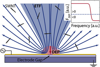
Electrophoresis describes the action of an electric field on fixed, net charges of particles. DEP, the focus of this review, on the other hand, only occurs when there are induced charges and only causes motion of polarized particles in a nonuniform electric field [which can be either direct current (DC) or alternating current (AC)]. Polarizability is a measure of the ability of a material to respond to an applied electric field and to produce charges at interfaces. A difference in charge density on either side of a particle in an applied nonuniform electric field gives rise to an effective or induced dipole across the particle. Particles move toward regions of highest electric field strength if the polarizability of the particles is greater than that of the suspending medium, otherwise they are repelled. At low frequencies, free charge movement is the dominant mechanism responsible for charging the interface, whereas at high frequencies, the polarization of bound charges (permittivity) dominates. This frequency dependence in the material behavior allows the selective manipulation of particles (Fig. 1).Reference Pohl4–Reference Morgan and Green6
The electrokinetic motion of nanomaterials suspended in solution is governed by bulk fluid flow (electrothermal flow) in more distant areas from the regions of highest electrical field strength (blue), whereas direct particle forces (dielectrophoresis) dominate nanomaterial motion inside the regions of highest field strength (red).Reference Burg, Bianco, Schneider and Poulikakos21 The attractive region is illustrated by the shaded areas for the respective force contributions. The frequency dependence of the dielectrophoretic force magnitude shown in the inset allows the selective manipulation of particles in different frequency regions.Reference Pohl4–Reference Morgan and Green6

The dielectrophoretic force is expressed as  when using the point effective dipole moment approach, where p is the effective dipole moment, v is the volume of the particle,
 is the complex effective polarizability, and E is the electric field.Reference Pohl4–Reference Morgan and Green6 The first work on DEP was carried out on polymer particles in 1951 by Pohl.Reference Pohl3 This work was followed by the successful manipulation of biological cells by Pohl and HawkReference Pohl and Hawk22 in 1966.
Moving toward ever smaller particles, progress was made by dielectrophoretically handling deoxyribonucleic acid,Reference Washizu and Kurosawa23 metallic nanowires,Reference Smith, Nordquist, Jackson, Mayer, Martin, Mbindyo and Mallouk24 multiwalled carbon nanotubes,Reference Yamamoto, Akita and Nakayama25 and ultimately SWNTs.Reference Chen, Saito, Yamada and Matsushige26 With smaller particle size, systematic particle control however becomes increasingly difficult as the dielectrophoretic force magnitude scales proportionally with particle volume and bulk fluid phenomena in the system start to play a role.
B. Fluid forces
Electric fields act on the particle-suspending medium when there are gradients in the fluid charge density, which can significantly impact small magnitude particle forces. Electrically induced fluid flow is subdivided into following two categories: electroosmosis and electrothermal flow (ETF).
Electroosmosis has its origin in the Coulomb force and is caused by the interaction of an electric field with free charges in the electric double layer. Charges in the diffuse layer migrate in the vicinity of an interface due to the applied electric field and generate a drag flow in the fluid. If the electric field is nonuniform, an AC signal induces analogous behavior on metallic surfaces.Reference Morgan and Green6, Reference Ramos, Morgan, Green and Castellanos27
Additionally, an electric current flows in the solution because of the applied electric field, causing Joule heating. Local heating of the fluid induces permittivity and conductivity gradients, thus creating a body force on the fluid, the so-called electrothermal force. Particles in the solution are subjected to motion by an imposed drag force from the ETF of the fluid.Reference Morgan and Green6, Reference Ramos, Morgan, Green and Castellanos27 Brownian motion has been shown to be less of an impediment to the dielectrophoretic movement of nanoscale particles.Reference Ramos, Morgan, Green and Castellanos27
C. Particle–fluid interaction
Predicting the movement of particles from a combination of the introduced forces is a rather complex task. First efforts to describe the dielectrophoretic behavior of carbon nanotubes focused on direct particle effects.Reference Dimaki and Bøggild28 Carbon nanotubes are generally modeled as prolate ellipsoids. By including ETF in the analysis, it became evident that electrically induced fluid flow plays a major role when manipulating nanoscale materials.Reference Lin, Shiomi, Maruyama and Amberg29 In a more comprehensive framework, involving all influences from imposed sinusoidal voltage potentials, namely DEP, electroosmosis, and ETF, it was shown that long-range nanomaterial transport is governed by hydrodynamic effects, whereas local trapping is dominated by dielectrophoretic forces in close proximity of the trapping site in low concentration dispersions (Fig. 1).Reference Burg, Bianco, Schneider and Poulikakos21
Numerous factors influence the results of the simulations. When nanomaterials are stabilized by surfactants in a solution, which is frequently the case for SWNTs, the entire nanomaterial/surfactant/double layer complex has to be taken into account to accurately determine the dielectrophoretic force. Surfactants induce a nonnegligible surface conductivity on insulating or semiconducting nanomaterials and, in these cases, the effective conductivity and permittivity of the complex must be considered in the force calculation.Reference Morgan and Green6 Frequency-dependent behavior is particularly affected by the induced surface conductivity. Also, for high aspect ratio nanomaterials in strong electric fields, the effective dipole approach may not be valid anymore to determine the dielectrophoretic force.Reference Lin, Shiomi and Amberg30 However, because the influence range of dielectrophoretic force is limited in dielectrophoretic deposition systems for nanomaterials dispersed in dilute dispersions, the exact force magnitude is usually not necessary for most practical DEP applications related to device and sensor integration.Reference Burg, Bianco, Schneider and Poulikakos21 On the other hand, this approximation may not be true anymore for highly concentrated solutions where an increased density of nanomaterials is expected to be in the vicinity of the deposition site. Further, flow patterns have been shown to change with respect to the applied field frequency, which may have considerable influence on the deposition yield.Reference Ramos, Morgan, Green and Castellanos27 All these aspects illustrate that the detailed understanding of the occurrence and interaction of each involved phenomenon is essential to increase the dielectrophoretic deposition yield on predefined electrode patterns and to improve the manipulation control of individual nanomaterials. In general, the predicted physical process behavior must be evaluated anew for every marked change in nanomaterial, solution, surfactant, concentration, or applied voltage.
III. SOLUTION PREPARATION AND QUALITY
The ability to dielectrophoretically deposit individual SWNTs and single-layer graphene is directly related to the quality of the prepared solution. Individually dispersed SWNT solutions and fully exfoliated graphene solutions must be available to ensure a high integration yield because the dielectrophoretic force scales directly with nanomaterial volume, causing bundles, agglomerations, and thick sheets to heavily favor their undesired deposition.
A. Individually dispersed SWNT solutions
Carbon nanotubes aggregate into bundles in aqueous solutions because of attractive van der Waals interactions and their hydrophobic nature. The most common method to separate nanotubes from bundles is using surfactants as an interfacial stabilizer to aid the dispersion. This stabilization technique was pioneered in 2002 with the observation of band gap fluorescence in surfactant-stabilized SWNT dispersions by O’Connell et al.Reference O’Connell, Bachilo, Huffman, Moore, Strano, Haroz, Rialon, Boul, Noon, Kittrell, Ma, Hauge, Weisman and Smalley31 SWNTs are highly exfoliated in these solutions, and large quantities of individual nanotubes can be observed by atomic force microscopy (AFM), whereas photoluminescence spectroscopy allows chirality assignment for semiconducting SWNTs.Reference Bachilo, Strano, Kittrell, Hauge, Smalley and Weisman32 The most common surfactants used in carbon nanotube research for long-term stable solutions are sodium dodecyl sulfate, sodium dodecylbenzene sulfonate, and sodium cholate.Reference Islam, Rojas, Bergey, Johnson and Yodh33, Reference Moore, Strano, Haroz, Hauge and Smalley34 By using atomic-structure-discriminating surfactants to engineer subtle differences in the buoyant densities of SWNTs and surfactants, an approach introduced by the Hersam group, density gradient ultracentrifugation (DGU), can be used to sort carbon nanotubes by diameter, band gap, and electronic type.Reference Arnold, Green, Hulvat, Stupp and Hersam35 In-depth reviews of the research on liquid phase exfoliation of SWNTs and toward monodisperse SWNT solutions are available.Reference Coleman36, Reference Hersam37
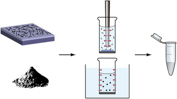
Typically, SWNT solution processing uses small-diameter purified nanotube products from bulk synthesis processes [for example, arc discharge, laser ablation, pulsed laser vaporization, high pressure carbon monoxide (HiPCO), or colbat-molybdenum-catalyst (CoMoCAT)] for subsequent dispersion. Upon device integration, however, these samples evidence comparably high contact resistance and low transmission.Reference Zhou, Kong and Dai38–Reference Chen, Appenzeller, Knoch, Lin and Avouris40 Therefore, when Ohmic behavior with low contact resistance and high device transmission are desirable, such as for individual SWNT-based electromechanical sensors, large-diameter SWNTs (>2 nm) with as few defects as possible are preferred. Large-diameter SWNTs are grown primarily by chemical vapor deposition processes and yield narrow-diameter distributions by controlling the size distribution of the catalyst particles.Reference Kong, Soh, Cassell, Quate and Dai41–Reference Durrer, Greenwald, Helbling, Muoth, Riek and Hierold44 These surface-synthesized SWNTs can be dispersed into surfactant-stabilized aqueous solutions by a short ultrasonic pulse (Fig. 2). The minimized processing, particularly the low-energy ultrasonic input to limit SWNT cavitation-induced scission and significantly reduce induced defects, as well as the avoidance of (oxidative) purification processes, results in high-quality SWNT dispersions.Reference Hennrich, Krupke, Arnold, Rojas Stütz, Lebedkin, Koch, Schimmel and Kappes45, Reference Burg, Schneider, Muoth, Durrer, Helbling, Schirmer, Schwamb, Hierold and Poulikakos46
Different approaches exist to disperse carbon nanotubes and exfoliate graphene into solutions ranging from changing the primary raw material, to purification, chemical treatment, energy input, and solvents. The most common techniques to prepare surfactant-stabilized dispersions are shown in the schematic.Reference Coleman36, Reference Hersam37, Reference Burg, Schneider, Muoth, Durrer, Helbling, Schirmer, Schwamb, Hierold and Poulikakos46

B. Exfoliated graphene solutions
A prerequisite for the dielectrophoretic graphene integration is the availability of solutions made up of individually dispersed graphene sheets in the micrometer size range. Chemically modified graphene oxide (GO) aqueous solutions, based on an oxidation protocol by Hummers and OffemannReference Hummers and Offeman47 in 1958, first provided these dispersions.Reference Stankovich, Dikin, Piner, Kohlhaas, Kleinhammes, Jia, Wu, Nguyen and Ruoff48 The nanomaterial consists of spReference Roukes2-bonded carbon sheets decorated with large numbers of covalently bonded hydroxyl and epoxide groups. The polar nature of the groups, coupled with the Coulomb repulsion associated with extensive proton dissociation, makes these dispersed GO sheets very stable in aqueous environments.Reference Li, Müller, Gilje, Kaner and Wallace49 However, due to the disruption in the π-orbital bond during oxidization, GO is a poor electrical conductor and subsequent reduction cannot completely remove the many structural defects introduced by the oxidation process.Reference Park and Ruoff20
Two methods, solvent-assisted and surfactant-assisted exfoliations, were pioneered by ColemanReference Coleman36 to disperse chemically unmodified graphene. It showed that graphite freely exfoliates into graphene in N-methylpyrrolidone and other solvents whose surface energy is well matched to that of graphene.Reference Hernandez, Nicolosi, Lotya, Blighe, Sun, De, McGovern, Holland, Byrne, Gun’ko, Boland, Niraj, Duesberg, Krishnamurthy, Goodhue, Hutchison, Scardaci, Ferrari and Coleman50 The high boiling points and viscosities often involved with these solvents, creating challenges in their further processing, have subsequently led to surfactant-stabilized aqueous graphene solution preparation, similar to SWNTs, yet with much milder sonication and centrifugation (Fig. 2).Reference Lotya, Hernandez, King, Smith, Nicolosi, Karlsson, Blighe, De, Wang, McGovern, Duesberg and Coleman51 More recently, the use of DGU in graphene solution preparation has been reported in making monodisperse dispersions.Reference Green and Hersam52
IV. SITE- AND TYPE-SELECTIVE GUIDED ASSEMBLY
DEP enables the selective deposition and directed movement of microscale and nanoscale objects in nonuniform electric fields. The electric field additionally aligns the randomly oriented SWNTs in the solution to assemble straight devices, thus minimizing curvature and bending effects.Reference Pohl4–Reference Morgan and Green6
A. Large-scale compatible experimental methods
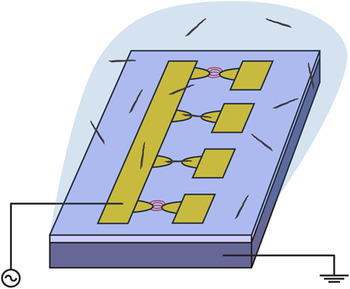
Samples for large-scale compatible dielectrophoretic assembly of individually accessible devices at very high integration densities are prepared by standard microfabrication techniques. Metallic electrodes are structured lithographically on an insulator covering a conductive substrate and provide electrical contacts for deposited nanomaterials (Fig. 3). Gap sizes are most frequently in the range of hundreds of nanometers to a few micrometers. Often the conductive substrate consists of doped silicon and the insulator is a grown silicon oxide layer. For large-scale integration purposes photolithography is preferred, while e-beam lithography enables higher pattern densities, narrower electrodes, and smaller electrode gaps. Narrower electrodes and smaller gaps favor higher dielectrophoretic deposition yields by reducing parasitic surface influences and increasing the electric field strength. Photolithography, on the other side, allows entire wafers to be patterned and processed at once, which can subsequently be diced into individual chips for easier handling. Thin film metal deposition is typically carried out by physical vapor deposition, either evaporation or sputtering, followed by photoresist lift-off or metal etching. Evaporation tends to yield much smaller surface roughness. The choice of metal is often related to the nanomaterial to be integrated. Optionally, electrodes can be embedded into etched pockets to reduce the step height of the electrode. No additional mask is necessary for this step, whereas slight directionality in the metal deposition practically limits the smoothness of the metal–insulator transition on the chip surface. By thoroughly cleaning the chips after fabrication in solvents and/or oxygen plasma, very clean, flat, and smooth surfaces can be obtained, which are necessary for topography analyses.
Capacitive electrode coupling of noncontacted counter electrodes (CEs) to a conductive substrate through an insulating layer allows the large-scale integration of individually accessible devices with minimal external connections while ensuring a self-limiting assembly mechanism and avoiding direct current throughput in the nanomaterials.Reference Burg, Bianco, Schneider and Poulikakos21, Reference Krupke, Hennrich, Weber, Kappes and Loehneysen53

DEP is performed by covering the fabricated sample with a thin film of nanomaterial solution and applying a sinusoidal potential to a single, so-called bias electrode (BE). This BE provides electrical contacts to numerous counter electrodes (CEs) which are individually accessible but remain floating (i.e., not connected) during the deposition process (Fig. 3). The ground connection is made directly to the conductive substrate. The CEs are so capacitively coupled through the insulator to the grounded substrate. With only two external connections, a very large number of electrode gaps can so be bridged during dielectrophoretic deposition. This minimized contacting is the essence of large-scale dielectrophoretic integration. Another important aspect is that current throughput through the nanomaterials is avoided during the deposition process, thus limiting processing effects in device fabrication. Applied frequencies range from tens of kilohertz to several hundred megahertz, depending on the electrical properties of the nanomaterial and solution as well as insulator thickness, with applied voltages in the range of a few volts, depending mostly on the gap size and dispersion concentration. This results in generated electric fields in the range of E rms ∼106–107 V/m between the capacitively coupled electrodes. The electric fields are highly localized in the vicinity of the electrode gaps and the strongest gradients occur close to the electrode edges. Dielectrophoretic processing times rarely last more than 1 min, after which the arbitrary function generator is turned off, then the sample is rinsed and optionally annealed at elevated temperatures to improve contact adhesion, also achievable through top-side metallization. Passivation of the devices with a protective layer, generally deposited by atomic layer deposition (ALD), ensures that the nanomaterials are not exposed to any further environmental and/or processing influences.Reference Helbling, Hierold, Roman, Durrer, Mattmann and Bright54
Identification of electrode-bridging nanomaterials is frequently performed by scanning electron microscopy at low acceleration voltages to minimize the risk of inducing any damage during visualization. Additional characterization can be carried out by AFM and electrical measurements. Deposition yields for individual carbon nanomaterials vary widely, but values in the range of 30% and higher are consistently reported. In unsuccessful deposition cases, no nanomaterials at all are observed, they are attached to only one electrode, or multiple distinguishable individual nanostructures bridge the gaps.
A self-limiting assembly mechanism exists in a narrow potential window, where the potential difference between bridged electrodes vanishes after an object deposits, disrupting the capacitively induced electric field and no additional nanomaterials are trapped. The potential equilibration between the electrodes is established by the inherent nanomaterial conductivity or the induced surface conductivity of the surfactants. When the applied potential or solution concentration is too high, the self-limiting mechanism is hindered, resulting in multiple deposits.Reference Burg, Bianco, Schneider and Poulikakos21 It is worth noting that multiple electrode contacting in one gap on three dimensionally structured samples is also possible by DEP, using a slightly adjusted design.Reference Schwamb, Choi, Schirmer, Bieri, Burg, Tharian, Sennhauser and Poulikakos55, Reference Schwamb, Burg, Schirmer and Poulikakos56
To accomplish the dielectrophoretic deposition of individual carbon nanomaterials, the applied electric potential parameters, frequency, voltage, and time have to be individually optimized for every different system of nanomaterial choice, dispersion solvent, and sample design. Currently, the choice of parameters, strongly influenced by factors such as gap size, insulator thickness, solution conductivity, nanomaterial characteristics, surfactant choice, and dispersion concentration, is still very much based on empirical optimization. No consistent method predicting these variables a priori has yet been found, and this topic requires further research. This lack of knowledge is the reason why used parameters are consistently noted in experimental reports.
B. Dielectrophoretic integration of SWNTs
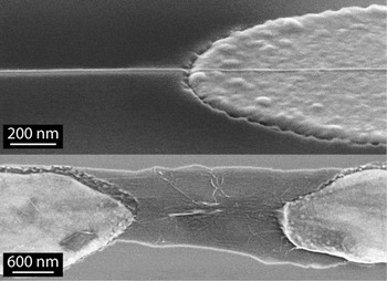
The simultaneous and controlled deposition of SWNTs onto a large number of lithographically fabricated (sub-)micrometer electrode pairs by AC DEP was pioneered by Krupke et al.Reference Krupke, Hennrich, Weber, Kappes and Loehneysen53 Their simple wiring scheme based on the capacitive coupling between the substrate and the electrodes showed to be independent of the number of contacts to be formed. The report also makes note of the self-limiting mechanism in forming single-nanotube devices. The ultra-large-scale integration (ULSI) of individual SWNT devices by DEP, which specifies at least 1 million transistors per chip, was achieved for individual SWNT devices a few years later.Reference Vijayaraghavan, Blatt, Weissenberger, Oron-Carl, Hennrich, Gerthsen, Hahn and Krupke57 Large-diameter SWNTs, which allow improved performance for sensor applications where high transmittance and Ohmic contacts are required, have been successfully assembled with a similar approach by using different SWNT raw materials and palladium (Pd) electrodes (Fig. 4).Reference Burg, Schneider, Muoth, Durrer, Helbling, Schirmer, Schwamb, Hierold and Poulikakos46 The dielectrophoretic integration of SWNTs, with the necessary preceding solution processing, has shown to induce few defects in the nanotubes, furthering the potential use of these high-quality components in nanoelectronic and sensor applications.Reference Stokes and Khondaker59, Reference Stokes and Khondaker60
Straight single-walled carbon nanotube (SWNT) and thin layer graphene oxide imaged in electron microscope after site-selective and large-scale compatible dielectrophoretic deposition. Detailed experimental conditions related to the structure design, solution preparation, and deposition parameters used to prepare these samples are documented in their corresponding reference.Reference Burg, Schneider, Muoth, Durrer, Helbling, Schirmer, Schwamb, Hierold and Poulikakos46, Reference Burg, Lütolf, Schneider, Schirmer, Schwamb and Poulikakos58

SWNTs come in two types, metallic and semiconducting, depending on their size and atomic structure, known as chirality.Reference Saito, Fujita, Dresselhaus and Dresselhaus61 This difference in electrical properties allows the type-selective manipulation of SWNTs in DEP under electric fields at particular frequencies. The dielectrophoretic separation of metallic SWNTs from semiconducting SWNTs was first demonstrated by Krupke et al.Reference Krupke, Hennrich, Loehneysen and Kappes62 in 2003 by selectively depositing thin films of highly enriched metallic carbon nanotubes at elevated frequencies. Follow-up studies on thin films confirmed the initial results by optical and electrical characterizations.Reference Krupke, Hennrich, Kappes and Löhneysen63–Reference Kang, Hong, Kim and Baik67 The surface conductivity induced by the surfactant on the SWNTs in the solution plays a primary role in the location of the dielectrophoretic crossover frequency where the dielectrophoretic separation takes place.Reference Krupke, Hennrich, Kappes and Löhneysen63, Reference Kim, Hong, Jung, Strano, Choi and Baik65–Reference Burg, Schneider, Bianco, Schirmer and Poulikakos68 The selective integration of individual large-diameter metallic SWNTs from heterogeneous solutions and their simultaneous deposition between electrodes was achieved in 2010, an important step toward site- and type-selective device integration of individual SWNTs.Reference Burg, Schneider, Bianco, Schirmer and Poulikakos68 An alternative approach for type-selective SWNT integration is to use smaller diameter chirality-enriched monodisperse SWNT solutions prepared by DGU.Reference Vijayaraghavan, Hennrich, Stuerzl, Engel, Ganzhorn, Oron-Carl, Marquardt, Dehm, Lebedkin, Kappes and Krupke69 In all cases, high-quality SWNT raw material, prepared solution, and contact interface are compellingly necessary to ensure a high integration and electrical characterization yield.
C. Dielectrophoretic graphene deposition
First evidence of dielectrophoretic manipulation of graphene-like material was given by the accumulation of micrometer-thick graphite oxide soot in an electric field gradient.Reference Hong, Jung, Kang, Kim, Chen, Stankovich, Ruoff and Baik70 This work was followed up by the deposition of single- and few-layer GO between electrodes by DEP using chemically modified exfoliated GO solutions (Fig. 4).Reference Burg, Lütolf, Schneider, Schirmer, Schwamb and Poulikakos58, Reference Wu, Sprinkle, Xuebin, Ming, Berger and de Heer71–Reference Burg, Schneider, Maurer, Schirmer and Poulikakos73 By choosing a silicon oxide layer thickness of 300 nm, single-layer deposits can be readily observed under an optical microscope.Reference Novoselov, Geim, Morozov, Jiang, Zhang, Dubonos, Grigorieva and Firsov15 The bridging over three dimensionally structured four-point electrodes was also shown to be possible.Reference Schwamb, Burg, Schirmer and Poulikakos56
The primary interest in graphene for electronics and devices resides in its pristine form. By using the in the meantime available exfoliated solutions of chemically unmodified graphene, the dielectrophoretic deposition of few-layers chemically unmodified graphene flakes was made feasible.Reference Burg, Schneider, Maurer, Schirmer and Poulikakos73, Reference Vijayaraghavan, Sciascia, Dehm, Lombardo, Bonetti, Ferrari and Krupke74 However, fully exfoliated and dispersed large sheet pristine graphene solutions are not yet available, thus limiting the dielectrophoretic integration yield and quality as the dielectrophoretic force is strongest for the largest and consequently thickest nanomaterials in the solution. To date, the dielectrophoretic deposition of a single layer of pristine graphene has not yet been achieved.
V. ADVANCED DEVICE AND SENSOR INTEGRATION
The promise of SWNTs and graphene as functional elements in nanoscale electronic devices, sensors, and applications, mostly fueled due to their ultra-small size, enhanced sensitivity, and extraordinary low power consumption, has driven research on these nanoscale materials to a large extent. Yet, the fundamental issue of scalable and reliable device fabrication remains one of the biggest challenges for effective commercialization of nanoelectromechanical systems. Ideally, a single SWNT or graphene flake is precisely placed at a predefined location and orientation, preferably bridging the ends of metallic leads.
Additionally, all process steps involved in the device and sensor fabrication must be scalable and compatible with each other. The selection of fabrication processes preceding and following the selective nanomaterial deposition may not be too restrictive, for example, due to high subsequent process temperatures. At the same time, potential adverse process effects to already integrated carbon nanomaterials, such as those likely resulting from ultrasound, polymer coatings, and plasma-assisted processes must be minimized.
DEP, which can easily be incorporated into standard microfabrication processes as outlined above, provides this prospect to fabricate advanced devices and sensors on a single chip in a large-scale manner, each individually accessible with customized functionality. In the following, research on individual SWNT and single-layer graphene-based electronic components, devices, and sensors assembled by DEP is reviewed.
A. Field-effect transistors
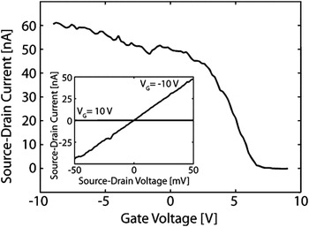
Semiconducting carbon nanotube behavior is analogous to that of a p-type metal–oxide–silicon field-effect transistor, except that the nanotube replaces silicon as the material that hosts the charge carriers (Fig. 5). The fabrication of SWNT-based field-effect transistors (CNFETs) does not require any alteration to the standard dielectrophoretic nanomaterial integration process, apart from a recommended passivation layer to improve long-term device stability. Elegantly, the conductive substrate of the sample, separated by the dielectric insulation layer from the SWNTs, acts as back gate in the three-terminal configuration. The first dielectrophoretically integrated CNFET was demonstrated by Krupke et al.Reference Krupke, Hennrich, Weber, Kappes and Loehneysen53 The high-density ULSI integration of individually accessible electronic devices was subsequently accomplished.Reference Vijayaraghavan, Blatt, Weissenberger, Oron-Carl, Hennrich, Gerthsen, Hahn and Krupke57 Solution-processed and dielectrophoretically integrated CNFET devices show high field-effect mobility and on-state conductance, important for nanoelectronic device applications.Reference Stokes and Khondaker59 Further, by using solution-processed SWNTs, their integration onto CMOS circuitry is possible because no high-temperature growth processes are involved, allowing for more elaborate electronic circuits and configurations.Reference Chen, Agarwal, Sonkusale and Dokmeci75 SWNT type-selective dielectrophoretic assembly substantially increases the yield of fabricated CNFET devices by avoiding the integration of metallic SWNTs, an import factor in device cost reflections.Reference Vijayaraghavan, Hennrich, Stuerzl, Engel, Ganzhorn, Oron-Carl, Marquardt, Dehm, Lebedkin, Kappes and Krupke69
The characteristic transistor behavior of a carbon nanotube field-effect transistor recorded after dielectrophoretic integration and contact annealing.Reference Burg, Schneider, Muoth, Durrer, Helbling, Schirmer, Schwamb, Hierold and Poulikakos46 No additional postprocessing is necessary. The conductive substrate of the sample is used for the capacitive CE coupling during the guided dielectrophoretic assembly and as a back gate during electrical characterization. The inset evidences the Ohmic contact behavior in the on-state of the large-diameter SWNT bridging Pd electrodes.

GO sheets assembled by DEP can be chemically reduced after integration to give rise to similar field-effect transistor behavior.Reference Joung, Chunder, Zhai and Khondaker76 Although performance characteristics and reliability does not match that of CNFET devices, this approach could prove to be important for the large-scale fabrication of functional electronic circuits based on two-dimensional crystals.
B. Chemical sensors
The high surface-to-volume ratio of SWNTs and graphene makes them promising candidates for the next generation of molecular chemical sensors. Room temperature operation is an additional advantage. In these devices, the transducer response is recorded electrically. As long as the carbon nanomaterial is exposed to the substance to be measured, the standard sample design for capacitively coupled dielectrophoretic integration can be used without modification, thus making their application and large-scale integration straight forward. Hydrogen sensing with DGU small-diameter- and chirality-sorted SWNTs integrated by DEP has been evidenced, originating from the hydrogen sensitivity of Pd-contacted Schottky barrier CNFETs.Reference Ganzhorn, Vijayaraghavan, Dehm, Hennrich, Green, Fichtner, Voigt, Rapp, Loehneysen, Hersam, Kappes and Krupke77 In addition, efforts to develop SWNT-based chemical gas sensors integrated by DEP onto CMOS circuitry have been reported, capable of detecting methanol and isopropanol.Reference Chen, Yang, Agarwal, Kim, Sonkusale, Busnaina, Chen and Dokmeci78 Selectivity of carbon nanomaterial chemical sensors, however, still remains as an issue.
C. SWNT-based piezoresistive pressure sensors
More advanced sensor concepts are based on electromechanical strain responses. SWNT-based strain sensing applications hold great promise in this field because of significantly enhanced sensitivity (gauge factor) and ultra-small size compared to state-of-the-art silicon-based sensors. Strain induces a bandgap change in SWNTs, which can be resolved by electric transport measurements.Reference Tombler, Zhou, Alexseyev, Kong, Dai, Lei, Jayanthi, Tang and Wu79, Reference Minot, Yaish, Sazonova, Park, Brink and McEuen80 The potential of SWNTs as functional transducer elements in classically designed piezoresistive pressure sensors was demonstrated by investigating the electromechanical behavior of SWNTs adhering to thin film membranes under small strain.Reference Grow, Wang, Cao, Wang and Dai81, Reference Stampfer, Helbling, Obergfell, Schoberle, Tripp, Jungen, Roth, Bright and Hierold82 The signal-to-noise ratio of the devices is highest in the off-state of small bandgap semiconducting (SGS) SWNTs, which consequently imperatively requires their individually accessible integration (T. Helbling et al., unpublished data).Reference Helbling, Roman and Hierold83
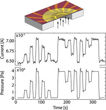
Making use of DEP for the site- and type- selective integration of individual SGS SWNTs, the large-scale compatible fabrication of ultra-small SWNT-based piezoresistive pressure sensors has been achieved (Fig. 6).Reference Burg, Helbling, Hierold and Poulikakos84 The carbon nanotubes are positioned on the edges of the membrane, the locations of highest strain. Because SGS SWNTs exhibit metallic permittivity behavior due to their small band gap, their selective deposition by DEP at high frequencies crucially increases the fabrication yield.Reference Burg, Schneider, Bianco, Schirmer and Poulikakos68 SWNT integration is followed by their encapsulation using a protective alumina layer deposited by ALD for long-term stability, the evaporation of a metallic top gate for transistor modulation, and back-side release of the thin-film small-diameter membrane. By providing sufficient deposition sites for selective dielectrophoretic integration, it can be ensured that every sample has at least one functional transducer. Further, multiple SWNTs can be envisioned to be combined together into a Wheatstone bridge configuration to cancel out temperature cross-sensitivity. The fabrication process can be scaled-up to make a large number of devices, showing great promise for commercially viable products, yet remains to be demonstrated.
Dielectrophoretically integrated SWNT-based piezoresistive pressure sensors show high sensitivity and good resolution at low power consumption (V sd = 50 mV).Reference Burg, Helbling, Hierold and Poulikakos84 Even the overshoots in the pressure chamber are recorded. The dielectrophoretic integration of the piezoresistive SWNTs is followed by traditional micromachining processes to fabricate the sensors. The fabrication scale-up of the long-term stable and robust devices is straight forward because of the exclusive use of large-scale compatible fabrication techniques.

D. Molecular electronics
More sophisticated concepts involve carbon nanotubes in molecular electronics to provide alternative approaches to further allow miniaturization beyond the foreseen limits of small-scale conventional silicon-integrated circuits. In this context, electroluminescence from the core of a rod-like molecule between two metallic SWNT electrodes, all assembled by DEP, has been reported to further advance this field of research.Reference Marquardt, Grunder, Błaszczyk, Dehm, Hennrich, Löhneysen, Mayor and Krupke85
VI. CONCLUSIONS AND OUTLOOK
From the above discussion, it becomes clear that so far only a limited number of carbon nanomaterial-based devices have been integrated by dielectrophoretic large-scale compatible fabrication techniques. Many more device concepts based on individual SWNTs and single-sheet graphene remain to be explored and further developed.
To date, traditional serial fabrication approaches have not been able to successfully commercialize individual carbon nanomaterial-based devices.Reference Baughman, Zakhidov and de Heer86 A major reason for this deficiency is the industrial unsuitability of the used processes. Large-scale compatible techniques, such as DEP, may be able to overcome this hurdle by providing simultaneous guided deposition on a large number of sites and avoiding high-temperature processes. Another challenge in the roadmap toward carbon-based electronics and sensors is the large variation between individual device performances. It is becoming more and more apparent that individual calibration is unavoidable.
Fewer graphene-based devices exist than SWNT-based devices, as a result of different reasons. First, the material has only recently been discovered; second, the precise electronic properties of the material are directly linked to its shape and edges, a feature which has proven to be extremely difficult to control; and third, fully exfoliated solutions containing large sheets are not yet available. A frequent question posed is whether SWNTs or graphene are more suited for applications. As it turns out, the answer to this question is closely related to the purpose of the device.Reference Yang, Ratinac, Ringer, Thordarson, Gooding and Braet87
The field of dielectrophoretic device integration is filled with opportunities, with the ultimate goal to drive functional devices toward large-scale low-cost commercialization operating at ultra-low power. To achieve this, the processes involved must be completely understood, experimental techniques must be controlled and mastered, and applications should be well chosen. New opportunities, such as novel materials, also appear on a regular basis.Reference Coleman, Lotya, O’Neill, Bergin, King, Khan, Young, Gaucher, De, Smith, Shvets, Arora, Stanton, Kim, Lee, Kim, Duesberg, Hallam, Boland, Wang, Donegan, Grunlan, Moriarty, Shmeliov, Nicholls, Perkins, Grieveson, Theuwissen, McComb, Nellist and Nicolosi88
ACKNOWLEDGMENTS
The authors thank Junichiro Shiomi for commenting on the manuscript. This work was supported by the ETH research commission (Grant No. TH-13/05-3).