Introduction
Metal-halide perovskites have garnered much attention for their rapid increase in single-junction record efficiencies to exceed 20% Reference Lee, Teuscher, Miyasaka, Murakami and Snaith1–Reference Green, Emery, Hishikawa, Warta and Dunlop3 (see the Introductory article in this issue). However, they deserve further serious consideration as the sole entry in a unique class of solar cell materials: solution-processable large-bandgap materials with small energetic losses. Previously, materials have met two of these criteria but not all three. Polymers are solution-processable large-bandgap materials, and indium-gallium-phosphide (InGaP) is a large-bandgap material with a small energetic loss. Reference Bett, Dimroth, Stollwerck and Sulima4 This classification makes metal-halide perovskites ideal for double-junction tandem cells.
Silicon is a market-leading photovoltaic technology and will probably continue in this role for the near future as the technology continues expanding while lowering its cost structure. However, silicon’s record efficiency has only increased from 25.0% to 25.6% in the previous 15 years, 5 asymptotically approaching its efficiency potential. As the overall cost of solar power shifts from a module dominated cost to a balance-of-systems dominated cost, improving the efficiency of installed modules becomes increasingly important. With greater efficiency, installing fewer modules reaches the same power target, reducing the balance-of-systems cost. A potential solution for improving the efficiency of modules is to make tandems.
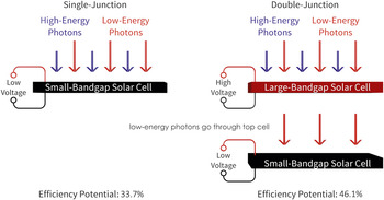
Tandems split the solar spectrum into parts. An absorber is most efficient when absorbing photons with energy equal to its bandgap. Photons with higher energy are absorbed but lose excess energy as heat, called thermalization. Tandems minimize the amount of thermalization with multiple absorbers responsible for sections of the solar spectrum rather than a single absorber responsible for the entire spectrum ( Figure 1 ).
Advantage of a tandem solar cell. A single-junction small-bandgap solar cell generates a low voltage from the available solar spectrum. A tandem uses a large-bandgap cell to absorb the high-energy photons, generating a larger voltage from these photons than the small-bandgap cell.

Single-junction solar cells are fundamentally limited to 33.7% efficiency, while double-junction tandems have a theoretical efficiency potential of 46.1%. A promising candidate for tandems is to use metal-halide perovskites to upgrade the performance of a commercially available solar cell, such as a silicon-based one. Reference Bailie, Christoforo, Mailoa, Bowring, Unger, Nguyen, Burschka, Pellet, Lee, Grätzel, Noufi, Buonassisi, Salleo and McGehee6–Reference Mailoa, Bailie, Johlin, Hoke, Akey, Nguyen, McGehee and Buonassisi8 The solution processability of metal-halide perovskites provides the potential for a low upgrade cost to an existing manufacturing plant. Metal-halide perovskites may also improve the commercial viability of a technology close to mass commercialization, such as copper indium gallium selenide (CIGS) Reference Bailie, Christoforo, Mailoa, Bowring, Unger, Nguyen, Burschka, Pellet, Lee, Grätzel, Noufi, Buonassisi, Salleo and McGehee6 or copper zinc tin sulfide (CZTS). Reference Todorov, Gershon, Gunawan, Sturdevant and Guha9
Tandem architectures
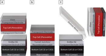
There are three main architectures to consider when designing perovskite tandems: mechanically stacked ( Figure 2 a), monolithically integrated (Figure 2b), and spectrally split (Figure 2c). Mechanical stacking means that the top and bottom cells are fabricated independently, then assembled together in the module. In monolithic integration, all layers are sequentially deposited on top of one another. Spectral splitting takes the independent fabrication of the mechanically stacked tandem one step further by using a wavelength-selective mirror to direct light to the appropriate cell such that the top cell no longer has to be transparent. The mechanically stacked tandem’s advantage is process and design flexibility. Independent fabrication allows previously developed single-junction design considerations to be applied to the tandem. The top and bottom cell strings in the module can be engineered to match the current or voltage between the strings, allowing for simple module construction and installation. Reference Bailie, Christoforo, Mailoa, Bowring, Unger, Nguyen, Burschka, Pellet, Lee, Grätzel, Noufi, Buonassisi, Salleo and McGehee6 Independent fabrication also enables separate binning of the sub-cells and therefore a larger processing window.
Tandem architectures. (a) Mechanically stacked tandem, (b) monolithically integrated tandem, and (c) spectrally split tandem. Note: CIGS, copper indium gallium selenide.

The monolithically integrated tandem’s advantages are efficiency and manufacturing cost potential. While the mechanically stacked tandem requires four electrodes, three of which must be transparent, the monolithically integrated tandem requires two electrodes, and only one must be transparent. Since transparent electrodes are not, in reality, perfectly transparent, removing two electrodes results in a higher practical efficiency potential. The manufacturing cost can be lower, as fewer layers need to be deposited.
The monolithically integrated tandem can be further subcategorized based on the intermediate layer used to electrically connect the two sub-cells. This intermediate layer could be either a band-to-band tunnel junction Reference Mailoa, Bailie, Johlin, Hoke, Akey, Nguyen, McGehee and Buonassisi8 or a recombination layer using a thin metal or transparent electrode to act as a recombination site. Reference Todorov, Gershon, Gunawan, Sturdevant and Guha9,Reference Ameri, Dennler, Lungenschmied and Brabec10 Band-to-band tunnel junctions are a proven option employed in III–V tandem solar cells, Reference Bauhuis, Mulder and Shermer11 while a recombination layer enables the use of heterostructured bottom sub-cells, such as a heterojunction with intrinsic thin (HIT) layer silicon cells or CIGS cells.
Spectral splitting Reference Uzu, Ichikawa, Hino, Nakano, Meguro, Hernández, Kim, Park and Yamamoto12 combines the advantages of mechanically stacked and monolithically integrated tandems, but a method of large-scale manufacturing is unclear. This architecture is likely feasible only in high-concentration systems due to the high cost of dichroic mirrors and the physical geometry of a spectrally split system. In these concentrator systems, relatively cheap mirrors are used to cover most of the land area and focus the light onto a smaller area, allowing small but expensive components to be more economically feasible.
Perovskite tandems are compatible with a range of small-bandgap materials
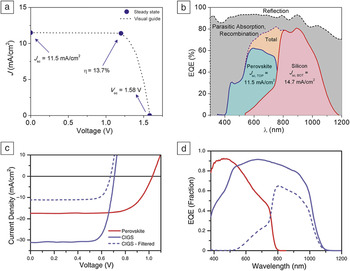
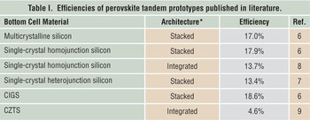
Several small-bandgap materials have been proposed and prototyped as bottom cells for perovskite tandems ( Figure 3 and Table I ). These include several variations of silicon: multicrystalline silicon, Reference Bailie, Christoforo, Mailoa, Bowring, Unger, Nguyen, Burschka, Pellet, Lee, Grätzel, Noufi, Buonassisi, Salleo and McGehee6 single-crystal homojunction silicon, Reference Bailie, Christoforo, Mailoa, Bowring, Unger, Nguyen, Burschka, Pellet, Lee, Grätzel, Noufi, Buonassisi, Salleo and McGehee6–Reference Mailoa, Bailie, Johlin, Hoke, Akey, Nguyen, McGehee and Buonassisi8 and HIT silicon. Reference Löper, Moon, Martín de Nicolas, Niesen, Ledinsky, Nicolay, Bailat, Yum, De Wolf and Ballif7 CIGS Reference Bailie, Christoforo, Mailoa, Bowring, Unger, Nguyen, Burschka, Pellet, Lee, Grätzel, Noufi, Buonassisi, Salleo and McGehee6 and CZTS Reference Todorov, Gershon, Gunawan, Sturdevant and Guha9 are also being explored. A potential bottom cell material that deserves study is a small-bandgap perovskite. A 0.9–1.1 eV bandgap solution-processable material has the potential for game-changing advances in cost, performance, and throughput of perovskite tandems.
Current density–voltage and quantum efficiency curves of monolithically integrated and mechanically stacked perovskite tandems. (a–b) Data for a monolithically integrated perovskite/silicon tandem. The voltages of the sub-cells add together producing about 1.6 V V oc, and current-density matching limits the current to 11.5 mA/cm2. Reproduced with permission from Reference 8. © 2015 American Institute of Physics. (c–d) Data for a mechanically stacked perovskite/copper indium gallium selenide (CIGS) tandem. There is no current-density matching requirement, allowing the current densities of the top and bottom cells to differ. The quantum efficiency for the CIGS cell when filtered peaks at 65% at 800 nm versus 87% when unfiltered due to the three transparent electrodes. Reproduced with permission from Reference 6. © 2015 Royal Society of Chemistry. Note: EQE, external quantum efficiency; J sc, short-circuit current density; η, quantum efficiency; λ, wavelength; V oc, open-circuit voltage; J sc,TOP, short-circuit current density of the top cell; J sc,BOT, short-circuit current density of the bottom cell.

Efficiencies of perovskite tandem prototypes published in literature.

* Stacked = mechanically stacked, Integrated = monolithically integrated.
Note: CIGS, copper indium gallium selenide; CZTS, copper zinc tin sulfide.
Modeling predicts high efficiencies
Metal-halide perovskites are not yet well characterized enough to provide true theoretical limitations. Optical modeling coupled with semi-empirical device assumptions offers the best predictions available today. Lal et al. Reference Lal, White and Catchpole13 considered a mechanically stacked perovskite/silicon tandem with a passivated emitter with rear locally diffused (PERL) silicon cell. A PERL cell is an advanced silicon cell architecture that passivates the top and bottom of the cell with silicon dioxide and creates a patterned rear electrode in order to reduce surface recombination on both the top and bottom surfaces. They estimated 36% peak efficiency with a 1.6 eV bandgap perovskite. They highlighted two main requirements to reach such efficiency. First, careful light trapping and management, particularly selective light trapping with a sharp reflective cutoff at the top cell band edge, are needed. Second, low-loss transparent electrodes with optimal transparency in the near infrared that can contact the perovskite cell without damaging it are required.
Löper et al. considered monolithically integrated and mechanically stacked perovskite/silicon tandems. Reference Loper, Niesen, Moon, Martin de Nicolas, Holovsky, Remes, Ledinsky, Haug, Yum, De Wolf and Ballif14 The silicon is modeled at its theoretical peak efficiency (29.4%). The perovskite is assumed to have a 1.6 eV bandgap and 21%–26% efficiency, depending on the modeled J sc. Assuming no front surface reflections, no parasitic absorption, and perfect Lambertian scattering, the peak efficiency for the mechanically stacked tandem is 37.2%. In the monolithic tandem, under current-density-matching constraints, the peak efficiency is 35.7%, assuming single-pass absorption in the perovskite top cell.
Challenges for attaining high efficiency
Challenges face perovskite tandems before the constraining assumptions in the models mentioned previously become the limiting constraints in real devices. The main challenges are heterojunction parasitic absorption, photon management, transparent electrodes, and bandgap tuning.
Heterojunction parasitic absorption
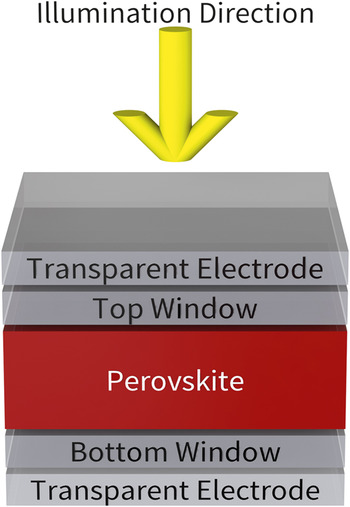
The perovskite sub-cell requires two heterojunctions with carrier-selective layers to reach high performance ( Figure 4 ). The primary purpose of these layers is to improve the electronic characteristics of the cell, but in a tandem, they must be transparent as well. One layer filters the light before it reaches the perovskite (termed top window), and the other filters the light after the perovskite layer (termed bottom window). The top window should have the largest bandgap possible to minimize parasitic absorption (absorption in the solar cell that does not contribute to photocurrent), but the bottom window may have a bandgap as small as the perovskite’s. In one common architecture, TiO2 (bandgap energy, E g = 3.2 eV) is the top window, and a small molecule, spiro-OMeTAD (2,2′,7,7′-tetrakis-(N,N-di-p-methoxyphenylamine)-9,9′-spirobifluorene E g = 3.1 eV), is the bottom window. Reference Burschka, Pellet, Moon, Humphry-Baker, Gao, Nazeeruddin and Grätzel15 In another common architecture, the top window, PEDOT:PSS(poly(3,4-ethylenedioxythiophene) poly(styrene sulfonate), absorbs broadly through the visible and infrared, and the bottom window is C60 or PCBM ([6,6]-phenyl-C61-butyric acid methyl ester, E g = 1.9 eV). Reference Malinkiewicz, Yella, Lee, Espallargas, Graetzel, Nazeeruddin and Bolink16
Schematic of a perovskite top cell showing the location of the top and bottom window layers with respect to the illumination direction.

The TiO2/spiro-OMeTAD architecture, with two large-bandgap windows, should not suffer from parasitic absorption. However, in working devices, spiro-OMeTAD is highly doped and absorbs throughout the ultraviolet, visible, and infrared, a common problem in doped organic semiconductors. Reference Nguyen, Bailie, Unger and McGehee17 For monolithically integrated tandems built with the standard architecture, the spiro-OMeTAD must be the top window due to processing constraints, which is devastating to cell performance. Reference Mailoa, Bailie, Johlin, Hoke, Akey, Nguyen, McGehee and Buonassisi8 Neither spiro-OMeTAD nor C60 are ideal materials as the top window in a tandem.
There are three strategies to minimize parasitic absorption in a layer. First, the layer may be replaced by a material without parasitic absorption. Second, the layer may be thinned to reduce the path length for absorption. Last, photonic engineering may be incorporated such that the electric field for photons of select frequencies is minimized within the absorbing layer. Reference Schueppel, Timmreck, Allinger, Mueller, Furno, Uhrich, Leo and Riede18 Only the first strategy provides a solution without tradeoffs. Therefore, alternate hole-selective and electron-selective heterojunctions with a bandgap >3.0 eV and minimal or no doped parasitic absorptions <3.0 eV are highly desirable.
Photon management
Absorption of all incident light is not easily accomplished. Perovskites have a reported diffusion length ≫1 μm, Reference Dong, Fang, Shao, Mulligan, Qiu, Cao and Huang19 the average distance a photogenerated carrier can travel before recombining, and is a factor that limits the thickness of solar cells. However, perovskite layer thicknesses are generally optimized to a few hundred nm in practice below the absorption depth—the path length required to absorb 63% of the light—for wavelengths close to the bandgap. The absorption depth for the methylammonium-lead-iodide perovskite is 398 nm for 750 nm photons and rises quickly to 855 nm for 770 nm photons. Reference Löper, Stuckelberger, Niesen, Werner, Filipič, Moon, Yum, Topič, De Wolf and Ballif20 In a tandem, a metal back reflector cannot be used to increase the effective path length of photons in the perovskite. Therefore, light trapping is necessary unless the perovskite layer is made substantially thicker. Monolithic tandems on silicon may take advantage of silicon front surface texturing to increase the effective path length of photons in the perovskite if the solution processing of the perovskite sub-cell can be made compatible with a rough surface. Selective reflectors and plasmonic structures are also potential solutions to this problem.
Transparent electrodes
The transparent electrode deposited on top of the perovskite sub-cell is critically important. Due to thermal- and solvent sensitivity, the perovskite is easily damaged during deposition of the transparent electrode. Two methods have been reported thus far, employing silver nanowires Reference Bailie, Christoforo, Mailoa, Bowring, Unger, Nguyen, Burschka, Pellet, Lee, Grätzel, Noufi, Buonassisi, Salleo and McGehee6 or indium tin oxide (ITO). Reference Löper, Moon, Martín de Nicolas, Niesen, Ledinsky, Nicolay, Bailat, Yum, De Wolf and Ballif7
Silver nanowires have proven to be compatible with perovskite processing and do not damage the underlying perovskite layer during deposition by adopting a room-temperature, solvent-free deposition. The nanowires are sprayed from solution onto a hot plastic film and subsequently physically transferred onto the perovskite cell at room temperature, separating the perovskite from direct exposure to the solvent and heating steps. As a mesh, the silver nanowire electrode relies heavily on the transport characteristics of the layer beneath it to transport locally generated charges to the nearest nanowire. Doped spiro-OMeTAD is conductive enough to serve this purpose. With changes to the top window envisioned, the new top window may not have sufficient lateral conductivity to be compatible with silver nanowire transparent electrodes. Many metals, including silver and gold, are also prone to forming insulating halide complexes. A barrier layer to ion migration between the halide source and the metal electrode should be developed for using metal electrodes.
ITO does not require lateral conductivity in the layer below it but has significant processing challenges. Sputter damage is a common problem when depositing ITO onto soft materials. Reference Meyer, Hamwi, Kröger, Kowalsky, Riedl and Kahn21 MoO x has been proposed as a transparent buffer layer to protect the cell, but current experimental evidence shows the underlying layers are still damaged during the sputtering process, and further improvements are required. Reference Löper, Moon, Martín de Nicolas, Niesen, Ledinsky, Nicolay, Bailat, Yum, De Wolf and Ballif7 Additionally, ITO improves its optoelectronic performance when annealed after sputtering. ITO is annealed at 190°C22 on HIT cells due to the limited thermal budget of amorphous silicon and can benefit from annealing at >300°C23,24 when no substrate temperature constraints exist. It is unclear if the methylammonium-lead-iodide perovskite can be stable at these annealing temperatures. To achieve peak optoelectronic performance of ITO, methods to improve the thermal stability of the perovskite are necessary.
1.8 eV bandgap stability
For optimal double-junction efficiency, a 1.8 eV bandgap top sub-cell material should be coupled with a silicon bottom sub-cell. Reference Bailie, Christoforo, Mailoa, Bowring, Unger, Nguyen, Burschka, Pellet, Lee, Grätzel, Noufi, Buonassisi, Salleo and McGehee6 Halide substitution tunes the methylammonium-lead-halide perovskite bandgap from 1.6 eV for methylammonium-lead-iodide to 2.3 eV for methylammonium-lead-bromide, and a 2:1 ratio of iodine to bromine yields a 1.8 eV bandgap. Reference Noh, Im, Heo, Mandal and Il Seok25 However, photo-instability in mixed-halide compounds prevents the extraction of a higher voltage from the higher bandgap material. Reference Hoke, Slotcavage, Dohner, Bowring, Karunadasa and McGehee26 This material must be stabilized or an alternative method of bandgap tuning must be discovered to reach optimal double-junction efficiency.
Conclusions
Metal-halide perovskites, as unique solution-processable large-bandgap semiconductors with small energetic losses, have the opportunity to be a breakthrough material in the photovoltaics field by pushing low-cost tandems beyond the single-junction theoretical efficiency. Initial tandem device models predict that 36%–37% efficiencies are achievable for perovskite/silicon tandems. If efficiency and stability challenges are overcome, perovskites may transform the photovoltaic field by enabling the first commercially competitive non-concentrated tandem modules.