I. INTRODUCTION
Resistive memory devices (RMDs), or resistive random access memory, are emerging devices for next-generation nonvolatile memory (NVM) applications due to their scalability, endurance, low operating voltage, and compatibility with complementary metal oxide semiconductor (CMOS) processing.Reference Waser, Dittmann, Staikov and Szot1–Reference Ouyang3 The basic structure of a RMD consists of an insulating material (I) sandwiched between two metal electrodes (M), which creates a switchable MIM structure. Devices are switched from the off state (or high resistance state, HRS) to the on-state (or low resistance state, LRS) by biasing one metal electrode and grounding the other in a process termed a set operation. During the set process, a current compliance, I COMP, is imposed to prevent the device from dielectric breakdown. The first set operation of the device may be termed a forming process if a larger voltage or I COMPis required for the first set than subsequent sets of the device. The reset operation occurs when the device is biased such that it transitions from the LRS to the HRS. If the set and reset occur in the same polarity (positive or negative voltage), the device is referred to as a unipolar device, while if the set and reset occur in opposite polarities, the device is known as a bipolar device. Devices that exhibit both unipolar and bipolar switching behavior are known as nonpolar devices.
Insulating materials that have been used within RMDs include metal oxides, perovskites,Reference Sawa4 and chalcogenides.Reference Wang, Tangirala, Raoux, Jordan-Sweet and Milliron5 Of these, numerous metal oxides have been extensively researched as potential candidates for RMDs including: TiOx,Reference Kwon, Kim, Jang, Jeon, Lee, Kim, Li, Park, Lee, Han, Kim and Hwang6 HfOx,Reference Briggs, Bishop, Capulong, Hovish, Matyi and Cady7 TaOx,Reference Miao, Strachan, Yang, Zhang, Goldfarb, Torrezan, Eschbach, Kelley, Medeiros-Ribeiro and Williams8 ZnOx,Reference Qi, Olmedo, Ren, Zhan, Zhao, Zheng and Liu9, Reference Van Nostrand, Cortez, Rice, Cady and Bergkvist10 CuOx,Reference Linn, Rosezin, Kügeler and Waser11, Reference Bishop, Bakhru, Novak, Briggs, Matyi and Cady12 NiOx,Reference Cagli, Nardi and Ielmini13 and SiOx.Reference Schindler, Thermadam, Waser and Kozicki14–Reference Rosezin, Meier, Breuer, Kügeler and Waser18 Silicon oxide RMDs have great potential for resistive memory applications because of the ubiquitous use of silicon oxide in traditional CMOS manufacturing. Tour et al.Reference Yao, Sun, Zhong, Natelson and Tour19–Reference Yao, Zhong, Natelson and Tour21 have demonstrated the resistive switching properties of silicon oxide using poly-Si/α-SiOx/poly-Si devices; in their devices, the memory function was facilitated by an etched vertical edge along the α-SiOx layer. More recently, advancements have been made in the use of SiOx materials for RMDs. Switching currents as low as 2 μA were observed using a similar device architecture (n-type Si/SiOx/p-type Si).Reference Mehonic, Cueff, Wojdak, Hudziak, Jambois, Labbé, Garrido, Rizk and Kenyon22 When copper has been utilized as an electrode (Cu/SiOx/Ir/W), write currents down to 1 nA have been achieved at room temperature.Reference Schindler, Weides, Kozicki and Waser23
In this work, we describe the use of hydrogen silsesquioxane (HSQ) as a novel precursor material for synthesizing SiOx in a RMD. HSQ is most commonly used as a negative tone electron beam resist. By virtue of its use in electron beam lithography (EBL), using HSQ to create SiOx opens up new avenues for fabricating metal–insulator–metal devices. In addition, because HSQ can be used to create SiOx at low temperatures, building SiOx-based RMDs on flexible plastic substratesReference Kim, Jeong, Kim, Choi and Lee24 becomes a realizable technology. To demonstrate the potential of devices fabricated from HSQ-based SiOx, switchable RMDs ranging in size from 100 μm to 48 nm were fabricated. The set and reset voltages were generally less than 5 V and resistance ratios of ∼101 to 102were achieved. From these data, we provide the groundwork for future development of HSQ-based switchable RMDs.
II. EXPERIMENTAL PROCEDURE
300-mm silicon wafers were used as the initial substrates for this work. SiO2/SiN was then deposited on top of the substrate using standard chemical vapor deposition (CVD) techniques. Cu, Ta, and TaN were then deposited by physical vapor deposition (PVD), acting as the electroplating seed, adhesion layer, and diffusion barrier, respectively. To create the bottom electrode (BE), 1 μm of electrochemically deposited Cu was grown on the Cu seed layer. The SiOx layer was fabricated by spinning 3% HSQ in methyl isobutyl ketone (MIBK) at 500 rpm for 1 min onto ∼1 in2 pieces cleaved from the 300-mm Cu wafer, followed by baking the substrates at 250 °C for 5 min. Microscale RMDs ranging from 100 to 10 μm2were fabricated using a metal shadow mask in which Ni top electrodes (TEs) were deposited to a thickness of 75–100 nm by electron beam evaporation.
Nanoscale devices on the order of 48 nm were fabricated using a damascene Cu via process. SiO2/SiN was deposited by CVD on top of the Cu/TaN/Ta/SiO2/SiN/Si substrates as detailed above, acting as the interlayer and etch stop, respectively. Vias ranging from 48 nm to 10 μm were then patterned by immersion lithography and etched into the SiO2/SiN by reactive ion etching. A Cu/Ta/TaN layer was deposited by PVD into the vias, to act as an electroplating seed, adhesion layer, and diffusion barrier, respectively. Cu was then electroplated to fill the vias, followed by chemical mechanical planarization to remove the Cu overburden and provide a smooth Cu via, flush with the SiO2. HSQ was then spun atop the Cu via wafers using the same conditions detailed above. A standard photolithography-based liftoff process was used to define microscale TEs above the Cu via BEs. Ni TEs were deposited with a thickness of 75–100 nm by electron beam evaporation.
X-ray diffraction (XRD) measurements were made with a Bruker D8 diffractometer (Bruker, Billerica, MA) equipped with a sealed copper x-ray source (40 kV, 40 mA) and a graded parabolic mirror at the x-ray source. The diffractometer was operated in a parallel beam geometry with Soller slits in both the incident and diffracted beam paths. A fixed angle of incidence of 0.5° was used for all scans with a detector step size of 0.05° per step and a count time of 10 s per step while scanning the detector from 10° to 90° for all scans. X-ray photoelectron spectroscopy (XPS) was performed using a XPS Thermo VG Scientific ThetaProbe (Thermo Fisher Scientific, Waltham, MA) with a 2.5 kV Ar sputter beam in conjunction with a standard Al Kα x-ray source and a helical electron detector to investigate the composition of the HSQ structure as a function of depth. Samples of pre- and post-250 °C baked HSQ on Cu before deposition of Ni TEs were analyzed to investigate the effects of annealing on Cu migration into the HSQ films. The specific XPS lines analyzed were: Cu 2p 3, O 1s, C 1s, and Si 2p.
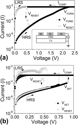
Current–voltage measurements were performed using an Agilent B1500A Semiconductor Device Analyzer (Agilent Technologies, Santa Clara, CA). Voltage sweeps for (re)setting of the devices were performed by biasing the Ni TE only in the positive voltage bias while keeping the Cu BE grounded to prevent migration of Cu into the HSQ film. See inset of Fig. 3(a) for schematic diagram of device structures and testing setup. The set voltage (V SET) was tabulated as the voltage at which current reached current compliance (I COMP). The reset voltage (V RESET) was tabulated as the voltage at which current passed below a predetermined threshold current (∼10−4 A) after reaching the maximum current (I MAX). Resistances were calculated for the R off and R on by taking the resistance value at 50 mV averaged among the two preceding and two subsequent resistance steps for each set and reset process. While endurance measurements were not explicitly performed for these devices, all devices switched at least 25 times to generate enough data to show distributions in switching characteristics. Box plots of each variable (V SET, V RESET, R off, and R on) were generated for each device, as well as monitoring each variable as a function of switch count.
Current verses voltage graphs from a 50 μm2 device showing (a) soft forming step with a V FORM of ∼2.3 V (I COMP = 10 mA), followed by a hard reset sweep with a V RESET ∼ 0.5 V. Inset in (a) is a cross-sectional diagram of a Ni/HSQ/Cu device in which the Ni TE is biased and the Cu BE is grounded. (b) Two curves showing the unipolar switching behavior that was common following the forming process in (a). Hard set and reset events are evident with V SET typically <1 V and V RESETon the order of 0.5 V for this device.

Cross sections of pre- and post-250 °C baked HSQ on Cu samples were prepared using a FEI Dualbeam 600 focused ion beam/scanning electron microscope (FIB/SEM; FEI, Hillsboro, OR) and mounted on Omnigrids for transmission electron microscopy (TEM) analysis before depositing Ni TEs. Briefly, the HSQ layer was protected using 100 nm of electron beam-deposited Pt followed by 2 μm of FIB-deposited Pt over an area of 10 × 3 μm. This region was isolated from the surrounding device structure by using a FIB to remove excess material leaving behind a lamella with protective Pt layers on top and mounted on an Omnigrid. Thinning was then performed from 3 μm to less than 100 nm by ion milling both the front and back sides with decreasing accelerating voltages from 30, 16, to 8 keV to clean the surface of the sample. TEM analysis was performed using a JEOL 2010F TEM (JEOL, Tokyo, Japan) operated at 200 keV, and bright field digital images were captured using a Gatan digital imaging system (Gatan Inc., Pleasanton, CA).
III. RESULTS AND DISCUSSION
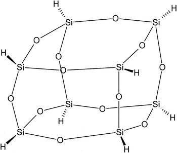
HSQ has a molecular formula of H8O12Si8. The structure of the HSQ molecule is a cubic-like cage with silicon atoms sitting at each corner. Three oxygen atoms and a single hydrogen atom are bonded to each corner silicon atom as shown in Fig. 1.Reference Yang and Chen25 The structural changes, which occur due to curing of the HSQ films, have been extensively studied.Reference Yang and Chen25–Reference Marcolli, Lainé, Bühler, Calzaferri and Tomkinson27 A redistribution of the cage network occurs from 250 to 350 °C, Si–H thermal dissociation occurs from 350 to 435 °C, and pore collapse occurs at temperatures greater than 435 °C. While not directly studied in this work, HSQ can also be cross-linked using EBL to create nanostructures.
Molecular diagram of HSQ cage structure. A silicon atom resides on each corner and is bonded to three oxygen atoms and a single hydrogen atom, leaving an open pore in the center of the structure.

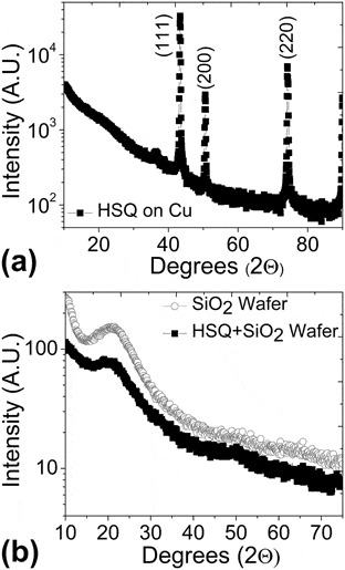
XRD was specifically performed at a low angle of incidence (0.5°) to investigate the near-surface crystallinity of HSQ after annealing at 250 °C. For XRD measurements only, 6% HSQ in MIBK was spun onto both Cu and SiO2 substrates to create a thicker HSQ film for surface analysis and reduce the affects of the substrate. Figure 2 shows that the HSQ was not crystalline after being annealed on a Cu substrate [Fig. 2(a)] or a 100-nm-thick thermally grown SiOx wafer [Fig. 2(b)]. The thermal oxide substrate was used in case the Cu substrate impacted the structure of the annealed HSQ. The peaks in the HSQ annealed on Cu spectra correspond to the (111), (200), and (220) Cu crystal planes. Figure 2(b) confirms the amorphous nature of the HSQ annealed on SiO2because the spectra does not show the formation of any additional diffraction peaks from HSQ after being annealed.
XRD results from (a) 6% HSQ on Cu spun at 500 rpm for 60 s and annealed at 250 °C for 5 min. Results show the (100), (200), and (220) diffraction peaks from the Cu substrate. There are no peaks from the HSQ layer, indicating a nominally amorphous atomic structure. (b) shows a comparison of a blank 100-nm thermally grown silicon oxide layer on silicon (black) compared to HSQ being spun onto the same thermally grown silicon oxide layer and annealed at 250 °C (gray). No additional diffraction peaks were observed with HSQ.

To investigate the switching properties of HSQ-based RMDs, V SET, V RESET, the resistance in the HRS (R off), and resistance in the LRS (R on) were measured. At least, two devices were tested from each device size over the scaled range (100 μm to 48 nm), resulting in a total of 31 tested devices. The inset in Fig. 3(a) shows a diagram of a HSQ-based device and a schematic of the applied voltage during setting/resetting. In this configuration, the Ni TE was biased positively and the Cu BE was grounded. Figure 3(a) shows an initial soft forming process that is representative of the RMDs fabricated in this work. This current–voltage (I-V) data were obtained from a 50 μm2 Ni TE device transitioning from the HRS to the LRS. The V FORM was taken as ∼2.3 V because this voltage corresponds to the point where the I COMP (10 mA) was reached. The forming process is termed “soft” because it refers to the gradual current increase in Fig. 3(a). While the majority of the devices tested exhibited a “soft” forming step, a small subset did exhibit a hard forming step. The observance of a soft versus hard forming step appeared to be a random occurrence from device to device and did not appear to scale with device size. The open circles in Fig. 3(a) show the subsequent hard reset process that occurred when the current dramatically transitioned from the LRS back to the HRS at V RESET = ∼0.5 V. Figure 3(b) shows two set/reset processes from the same 50 μm2 device after the initial forming and reset in Fig. 3(a). Figure 3(b) also shows two additional properties typical of HSQ-based devices. First, the I COMP required during forming (10 mA) was an order of magnitude higher than that needed in the subsequent set processes (1 mA). The second property shown in Fig. 3(b) is that the set voltages were typically less than the initial forming voltage.
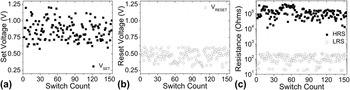
While Fig. 3 only shows three set/reset processes for a single 50 μm2 device, the V SET, V RESET, R on, and R off are plotted as a function of switching cycle in Fig. 4. From Fig. 4(a), a clear voltage threshold for all set processes is observed at ∼0.6 V. At voltages below this value, the device would not set. It was also observed that the largest voltages required to set this 50 μm2 device did not exceed 1.25 V after the soft forming step (∼2.3 V). As shown in Fig. 4(b), 0.6 V was the largest voltage needed to reset the device. For the majority of switching events, the reset voltage ranged between 0.25 and 0.6 V. One additional property of note for these devices is that the set voltage was typically greater than the reset voltage (V SET > V RESET). The observation of V RESET being lower than V SET has been shown elsewhere in the published literature. Kim et al.Reference Kim, Jeong and Hwang28, Reference Kim, Choi, Koo, Choi, Jeong and Hwang29 described similar device behavior with V RESET being less than V SET due to the thermal dissolution of the conducting filament, despite different oxide and electrode materials. When comparing the R off and R on as a function of switch count [Fig. 4(c)], the R on ranges between 10 and 300 Ω for all switches of the device, while the R off for the device falls between 104 and 5 × 10⁵ Ω. The ratio of R off/R on is known as the memory window, which is a measure of the resistance difference between the lowest R off and the highest R on. For the 50 μm2device, the memory window is greater than 10, which is the minimum requirement for most RMD applications allowing for easy differentiation between states when reading the device at low voltages.Reference Waser, Dittmann, Staikov and Szot1
Endurance plots showing (a) V SET, (b) V RESET, and (c) R off/R on versus switch count. A threshold voltage of ∼0.6 V distinguishes V SET from V RESET. The set processes occurred at voltages greater than or equal to this threshold value, and reset processes occurred at voltages less than or equal to the threshold voltage. A similar threshold resistance occurred for the R on in which the R onfor all switches was greater than 10 Ω and less than 300 Ω.

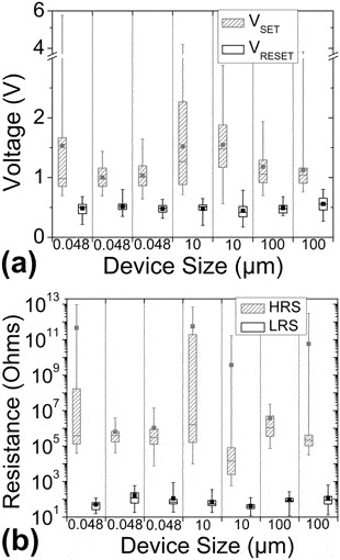
To compare how these switching parameters scale as a function of device size, Fig. 5 shows box plots for the (a) V SET and V RESET and (b) R off and R on for multiple devices that scale more than three orders of magnitude. Each box represents the 75%/median/25% quartiles and shows the minimum and maximum of the dataset for each device (lowest and highest horizontal line) along with the calculated average (filled square). Figure 5(a) shows the V SET and V RESET for 100 μm, 10 μm, and 48 nm devices, where V SET was less than 3 V and V RESET was less than 1 V for most switching cycles, independent of the device size. While V SET varies more dramatically than V RESET, neither voltage appears to scale with device size. The average V SET and average V RESET for all device sizes were ∼1.2 and 0.5 V, respectively. While some devices showed clear voltage demarcations between all set and reset processes at specific voltages [Figs. 4(a) and4 (b) at 0.6 V and Fig. 5(a)], looking closely at Fig. 5(a), there is an overlap in switching voltages for the maximum V RESET and minimum V SET voltages for at least one device of each size. This occurred randomly in roughly half of all device sizes tested (data not shown) and was not a function of device size. For RMDs to be implemented as NVM devices, V SET occurring from hundreds of millivolts to a few volts is advantageous over the large voltages required for current flash memory.Reference Waser, Dittmann, Staikov and Szot1 When comparing the R off and R on for devices across the device size range, Fig. 5(b) shows a distinct memory window (>10) for devices of all sizes. It has been estimated that the R off/R on ratio should be greater than 10 to be used with current sensing amplifiers to distinguish the two states for implementation as NVM devices. In most cases, the memory window for HSQ-based devices is on the order of 10–100. Figure 5(b) also shows larger variations in the R off than the R on for all devices. Higher set voltages are required for switches having a large R off when comparing V SET in Fig. 5(a) to the R off in Fig. 5(b). Knowing the desired switching parameters for RMDs, the observed characteristics of the 50 μm2 device outlined in Fig. 4 and scaling of devices from 100 μm2 to 48 nm2 in Fig. 5 meet many of these desired criteria for RMD implementation.
Box plots showing (a) V SET/V RESET and (b) R off/R onfor device sizes of 100 μm, 10 μm, and 48 nm. These plots demonstrate the scalability of HSQ-based devices and the lack of a statistical change in the device properties across the three orders of magnitude change in device size.

When comparing the HSQ-based RMDs to those in literature, Tour et al.,Reference Yao, Sun, Zhong, Natelson and Tour19−Reference Yao, Zhong, Natelson and Tour21 poly-Si/SiOx/poly-Si required 8–10 V set pulses and 4–5 V reset pulses with R off/R on ratio of ∼1010:105, similar n-type Si/SiOx(Si rich)/p-type Si devices switch using bipolar pulses at ±20 V and unipolar pulses at −12 and −8 V for setting and resetting, with R off:R on of 1010:105 for bipolar devices and 107:105 for unipolar devices.Reference Mehonic, Cueff, Wojdak, Hudziak, Jambois, Labbé, Garrido, Rizk and Kenyon22 In nonsymmetric devices (Cu/SiO2/Ir/W), setting occurs at less than 0.5 V with an I COMP of 1 nA and resetting of the device occurs at less than −0.25 V and corresponds to a R on of ∼108 for sub-100-nm devices.Reference Schindler, Weides, Kozicki and Waser23 Compared to previous work, HSQ-based devices presented in this paper have the added benefit of requiring less voltage for both setting and resetting of the device compared to symmetric SiO2 devices, with a shift toward lower resistance values for both the R off (∼106) and R on (∼102) of both the symmetric and nonsymmetric devices. HSQ devices have V SET generally less than 3 V and V RESET less than 1 V for a majority of switches, with a R off/R onratio of at least 10 and many times 10–100 for most device sizes.
Because it is well known that Cu can diffuse readily through SiOx,Reference Loke, Yue, Cho and Wong30–Reference He and Lu33 it is likely that Cu from the BE could be playing a role in the above described switching properties.
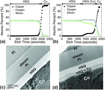
Composition–depth profiling via XPS analysis was performed in Fig. 6(a) on an unannealed sample of HSQ on Cu and Fig. 6(b) on an annealed sample of HSQ on Cu at 250 °C for 5 min. The unannealed sample in Fig. 6(a) shows at 50:50 mixture of Si:O present throughout the HSQ film until ∼1700 s, at which time there is small layer of copper oxide present at the HSQ/Cu interface. No Cu was detected in the HSQ layer, as measured by XPS. Compared to the annealed sample [Fig. 6(b)], it was observed that a 50:50 ratio of Si:O is present until ∼1000 s, at which point a decrease in the Si composition corresponds with an increase in O composition until ∼1300 s. At this time, a noticeable increase in the atomic composition of Cu was observed from 1300 to 2000 s reaching a maximum atomic composition of ∼8% in the HSQ film [represented by HSQ(Cu) on the top axis in Fig. 6(b)] and consists of a mixtures of Si, O, and Cu before reaching the Cu surface near 2250 s. As with the unannealed sample, there is a CuOx layer, which forms close to the Cu surface as the presence of Si begins to decrease. XPS species were analyzed at Cu 2p 3, O 1s, C 1s, and Si 2p, and no binding energy shifts were observed. This composition change and Cu migration were confirmed by taking TEM cross sections from each sample as seen in Figs. 6(c) and 6(d). Figure 6(c) shows the unannealed HSQ/Cu sample with Pt/e-beam Pt protective layers used for sample preparation and no Cu migration into the HSQ film. After annealing a HSQ/Cu sample at 250 °C, Fig. 6(d) shows some Cu, which migrated ∼1/3 of the way into the HSQ film and increased the Cu composition. Selected area diffraction was performed of the HSQ alone showing the amorphous nature of the HSQ confirming results from Fig. 2(b) (data not shown). Similar results were obtained and confirmed using secondary ion mass spectroscopy (SIMS) (data not shown), in which an increase in Cu composition into the HSQ layer occurs after annealing the sample.
XPS depth profiles of HSQ on Cu (a) before and (b) after hard baking at 250 °C. Unintentional copper doping up to ∼8 at.% is evident in the HSQ film after the hard bake. TEM cross section of HSQ on Cu (c) before and (d) after hard baking at 250 °C. The copper-doped interfacial layer is shown between the HSQ layer and Cu BE.

Previous results using SiOx as a RMD have shown that conduction can occur by either silicon nanocrystals (nc-Si) or through the formation of a metallic filaments based upon the electrodes used for device fabrication. To distinguish a nc-Si filament from a metallic filament, studies were performed on devices set into the LRS by measuring resistance changes at 50 mV as a function of temperature starting at 300 K and decreasing to 175 K in 25 K increments (data not shown). Conduction through a metallic filament would cause an increase in R on with increasing temperature due to enhanced phonon scattering at elevated temperatures. This is contrary to a nc-Si filament, which would exhibit a decrease in resistance with temperature because of its semiconducting nature. Data collected from five devices from 100 to 60 μm2 at 10 μm2 increments showed an overall increase in resistance as a function of temperature from 175 to 300 K, though none could be fit to a pure metallic filament composed of Ni, Cu, NiSi, Ni2Si, or Ni31Si12 using the corresponding temperature coefficient of resistance (TCR). The increase of Cu concentration in the HSQ film after annealing may explain why none of the R on versus temperature data could be fit to the pure metallic filaments listed above due to the formation of a mixed type NixCuySizReference Zhi-yong and Ming-pu34, Reference Stobrawa, Rdzawski, Głuchowski and Malec35 filament having a different TCR. It should be noted that resistivity increases as feature size decreases due to increased grain boundary scattering, and no analysis of filament size has been performed at this time. Non-HSQ-based SiO2 switching on Cu has been observed in literature without XPS or TEM analysis of what occurs at the Cu–SiO2 interface. Waser et al.Reference Schindler, Thermadam, Waser and Kozicki14 have observed that thermal annealing of SiO2 on Cu at 610 °C is required for their devices to switch. These Cu-based SiO2 devices generally have lower switching voltages (< 1.5 V) than non-Cu-based devices generally requiring switching voltages from 5 to 20 V. The Cu/HSQ interlayer observed here may act as an extended BE reducing the true HSQ thickness from 100 to ∼55 nm, resulting in shorter conducting filaments necessary to traverse from the Ni TE to the Cu/HSQ interlayer, requiring less voltage to set and reset the device. Thus, the Cu electrode used herein and elsewhere in literature may play a role in switching voltages observed for setting and resetting of devices due to Cu interlayer formation compared to SiO2devices using a poly-Si source. While neither XPS nor SIMS would be able to detect a conducting nanofilament due to its size, further analysis is required to determine the composition of any conducting filaments present and determine an accurate conduction mechanism of these devices.
IV. SUMMARY AND CONCLUSIONS
HSQ is commonly used as a negative tone resist in EBL. This material has been used to create SiOx-based RMDs through a spin-on/bake process. These devices exhibited positive unipolar resistive switching with V SET and V RESET values generally less than 3 V and less than 1 V, respectively, and a memory window typically greater than 10. Functioning RMDs ranged from 100 μm to 48 nm in size, demonstrating the scalability of these devices. There was no statistical change in the V SET, V RESET, R off, and R on over this range of device sizes. Compared to previous work, the HSQ-based devices presented in this paper require a lower voltage for both setting and resetting. The R on values for HSQ RMDs showed a positive deviation versus temperature, suggesting that the on-state conduction is dominated by a metallic filament as well as no area dependence in R on. Although copper migration was observed into HSQ films by XPS and TEM in support of the temperature data, further work is needed to determine if a filament is indeed controlling the setting and resetting behavior of these HSQ-based devices. In conclusion, HSQ is an excellent precursor for synthesizing SiOxthat exhibits resistive memory behavior. Further, this work demonstrates a spin-on resistive memory material that adds to the already expansive list of oxides used in RMDs.
ACKNOWLEDGMENTS
This research was sponsored by the Air Force Research Laboratory Grant No. FA8750-11-1-0008. The authors would like to acknowledge the Center for Semiconductor Research at CNSE for wafer development and Dr. Joseph Van Nostrand, AFRL-RI, for programmatic/scientific support. The authors would like to thank Dr. Steve Novak for SIMS measurements, Dr. Richard Matyi for XRD measurements, and Dr. Ji Ung Lee and Mr. Everett Comfort for the temperature-based I-V measurements.