Hopes and prospects for quantum Hall effect metrology using graphene
Metrological context
Metrology aims to establish definitions and representations of units, with the constraint that they be as universal and as convenient as possible so that they can be easily used both by scientists and in industry. In terms of universality, the discovery of several quantum phenomena in solids has revolutionized electrical metrology in the past few decades. Based on the Josephson effect and the quantum Hall effectReference Klitzing1 (QHE), the volt and the ohm have been represented since 1990 in terms of only Planck’s constant h and the electron charge e, which is preferable to the use of material artifacts (namely, Weston standard cells for the volt and resistors for the ohm).
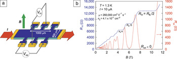
The resistance standard is based on the initially surprising observation that the transverse resistance, R H ≡ Rxy, of a two-dimensional electron gas (2DEG) placed in a perpendicular magnetic field B (strictly speaking magnetic induction) (see Figure 1a) is quantized at rational fractions of the von Klitzing constant, R K ≡ h/e 2. At the same time, the longitudinal resistance, Rxx, drops to zero, reflecting the absence of dissipation in the 2DEG (Figure 1b).
(a) Drawing of a typical Hall bar, fabricated from a two-dimensional electron gas (formed in a GaAs/AlGaAs heterostructure, for example). (b) At a temperature of T = 1.3 K, when the perpendicular magnetic field B is increased, the Hall (transverse) resistance R H, defined as the ratio of the transverse voltage V H to the current I, shows plateaus at values R K/i, where i is an integer and R K theoretically equals h/e 2. Simultaneously, the longitudinal resistance (Rxx = Vxx/I, where Vxx is the longitudinal voltage) drops to zero. The value of the Hall resistance on the plateaus is a very reproducible (deviations of <10–10) resistance reference. n s, carrier density; μ, carrier mobility.

This integer quantum Hall effect relies on the charge carriers in the system occupying a series of discrete energy levels known as Landau levels (LLs), which correspond to the quantization of the cyclotron motion of charge carriers in the magnetic field. The value at which R H is quantized depends on the number of filled LLs, described by the filling factor ν = n sh/eB, where n sis the carrier density.
The universal character of the quantum Hall resistance standard is supported by very strong theoretical arguments.Reference Poirier and Schopfer2 Nonetheless, it is critical for dependable metrology that this universality be experimentally validated.
The quantum resistance standard is based on a Hall bar usually fabricated from a 2DEG formed in a GaAs/AlGaAs semiconductor structure (Figure 1a). When operated at low temperature (T ≤ 1.5 K) and high magnetic field (B ≈ 10 T), with measurement currents of a few tens of microamperes on the R H plateau at R K/2 (ν = 2), such a Hall bar allows the calibration of a wire resistor in terms of a conventional value of R K (i.e., 25,812.807 Ω) with a typical accuracy of 10–9. This performance is possible owing to specific instrumentation based on a resistance comparison bridge equipped with superconducting transformers (cryogenic current comparator, CCC) and superconducting quantum interference devices (SQUIDs). The realization of the primary resistance standard with the QHE improved the reproducibility by three orders of magnitude over the previous 10–6.
A present challenge in metrology is to generalize the use of quantum electrical standards by improving their dissemination closer to end users and extending their application range (e.g., standards with wider ranges of values and usable frequencies), with the goal of better traceability of electrical units. An important development has been arrays of quantum standards with larger value ranges that better match the values needed in particular applications, thereby shortening the calibration chain and reducing the final uncertainty. For example, so-called quantum Hall array resistance standards (QHARS), with accurate values ranging from 100 Ω to 1.29 MΩ, have been successfully developed by connecting several tens of single Hall bars in parallel and in series.Reference Poirier, Bounouh, Hayashi, Fhima, Piquemal, Genevès and André3 Much remains to be done to make dissemination of quantum standards more convenient.
Moreover, because of their direct link to h and e, the electrical quantum standards furthers the goal of a revised Système International (SI) with units based on fundamental physical constants.Reference Piquemal and Jeckelmann4 This effort involves establishing new definitions of several base units by fixing the value of some fundamental constants (h, e, the Boltzmann constant [k B], Avogadro’s number [N A]), as was previously done for the speed of light (c) to define the meter. Achieving this goal requires more accurate determinations of fundamental constants and relevant tests of the underpinning quantum physics. One essential step in this effort is the redefinition of the kilogram, for example, using the watt balance.Reference Eichenberger, Genevès and Gournay5 This device measures the mechanical power of the displacement of a mass in the gravitational field in terms of an electrical power, which is, in turn, calibrated using the QHE and the Josephson effect. Assuming notably that R K = h/e 2, it establishes a link between Planck’s constant and the mass unit. QHE universality tests are also very usefulReference Poirier, Schopfer, Guignard, Thevenot and Gournay6 because they can point out any nonuniversal correctionReference Penin7, Reference Penin8 of R K to h/e 2. The discovery of the QHE in graphene opens the way not only to a better and more convenient quantum resistance standard but also to new fundamental tests of the physics that underpins quantum electrical metrology.
Quantum Hall effect in graphene
Graphene, a one-atom-thick layer of carbon atoms, is a semiconductor with two valleys in its electronic band structure and zero gap between the conduction and valence bands, enabling both holes and electrons to be involved in charge transport (Figure 2a, left). The fascinating electron-transport properties of graphene originate from the honeycomb lattice of carbon atoms in which charge carriers at low energy behave as chiral, massless, relativistic fermions. In addition, the two crystallographic sublattices that can be defined endow carriers with an extra spinlike degree of freedom (called pseudospin), which results in an extra “Berry’s phase” of π in the case of a 2π rotation of the momentum.Reference Neto, Guinea, Peres, Novoselov and Geim9
(a) Low-energy electronic band structure as a function of in-plane momentum components kx and ky for monolayer graphene, showing conical electron (red) and hole (blue) bands meeting at the Dirac point (left) and the sequence of Landau levels (LLs, right), indexed by the integer n, with energies  $E_n^ \pm $ and energy gaps ΔE, formed at high magnetic field. The degeneracy 4eB/h of the LLs is twice that in common semiconductors such as GaAs, and there is an LL at zero energy. (b) Magnetic-field dependence of the energy gaps (ΔE, left scale) and equivalent temperatures (T, right scale). Gaps shown for monolayer graphene separate the n = 0 LL from the n = ±1 LLs (dark blue, protecting the ν = ±2 quantum Hall states) and the n = ±1 LLs from the n = ±2 LLs (light blue, ν = ±6). The gap shown for bilayer graphene (green) separates the degenerate n = 0, ±1 LLs from the n = ±2 LLs (ν = ±4). For GaAs, the cyclotron gap (red) is independent of the LL filling factor ν. The horizontal line corresponds to the empirical energy gap value ΔE = 80k BT at T = 4.2 K that should ensure R H quantization at 10–9 accuracy. The value of the energy gap in monolayer graphene at ν = 2 is much larger than that in GaAs at low magnetic field. DOS, density of states; v F, Fermi velocity; h, Planck’s constant; k B, Boltzmann constant.

One consequence of this Dirac physics is the appearanceReference Novoselov, Geim, Morozov, Jiang, Katsnelson, Grigorieva and Firsov10 of resistance plateaus at R H = ±R K/[4(i + 1/2)] = ±R K/2, ±R K/6, ±R K/10, ... (for integer i ≥ 0), where the first plateaus at ±R K/2 survive even at room temperature.Reference Novoselov, Jiang, Zhang, Morozov, Stormer, Zeitler, Maan, Kim and Geim11 Under a magnetic field, the density of states forms a series of discrete LLs with 4eB/h degeneracy, twice that in GaAs, because valley degeneracy adds to spin degeneracy. In addition, rather than being proportional to B, the LL energies are proportional to B 1/2, being given by  $ \pm v_{\rm{F}} \sqrt {2\hbar neB} $, where n is the LL index and νF is the Fermi velocity of the charge carriers (Figure 2a). It also appears that LL energies depend on the square root of the LL index, so that, for increasing LL filling factor, the gap between the last occupied LL and the first unoccupied LL decreases at a given induction (Figure 2b). The QHE in graphene is especially robust on the first plateau (ν = ±2), because the energy spacing of
 $36\sqrt B $ meV/T0.5 between the first two LLs (n = 0 and n = 1; spin and valley degenerate) is larger than that in GaAs (1.7B meV/T) particularly at low magnetic fields (Figure 2b).
In bilayer graphene consisting of two graphitic monolayers with Bernal (AB) stacking, the dispersion relation becomes parabolic, and carriers behave as chiral massive Dirac fermions with a Berry’s phase of 2π and a mass of m = 0.033m e, where m e is the electron mass.Reference Nilsson, Castro Neto, Guinea and Peres12 This leads to a QHE with resistance plateausReference Novoselov, Geim, Morozov, Jiang, Katsnelson, Grigorieva and Firsov10 at R H = ±R K/[4(i + 1)], for integer i ≥ 0. The energy gap between LLs occurring at  $ \pm \hbar {\rm{\omega }}_{\rm{c}} \sqrt {n(n - 1)} $ (where ωc = eB/m is the cyclotron frequency) is smaller than that in single-layer graphene, especially at low magnetic fields, but it is larger than that in GaAs systems.Reference McCann and Fal’ko13
Figure 2b compares the energy gaps, ΔE, between the first Landau levels in monolayer graphene, bilayer graphene, and GaAs. It notably shows that the value of ΔE at 10 T in GaAs is reached in monolayer graphene at only 0.2 T.
The larger energy gaps give much hope that a resistance standard operating at higher temperature, lower magnetic field, and/or higher measurement current than in GaAs while keeping the same accuracy of 10–9 or better could be developed in both graphene systems (but with a net advantage for monolayer graphene, especially at very low B).
A relevant QHE quantization criterion is ΔE(B) ≫ k BT, which is based on the thermal activation of carriers across the gap. In GaAs Hall bars, it has been observed that a gap of ΔE ≈ 80k BT should ensure R H quantization with 10–9 accuracy. By this criterion, in monolayer graphene, one can expect R H quantization at R K/2 with 10–9 accuracy at 4.2 K for all fields above 1 T because the energy gap between the n = 0 and n = 1 LLs is already equivalent to 462 K at this magnetic field. The robustness of the QHE against measurement current is also improved by the larger LL gap, which reduces current-induced inter-LL transitions, whether caused by direct electric field effects or by heating. Measuring R H with higher currents improves the signal-to-noise ratio and reduces the uncertainty in the R Hmeasurement.
If the more robust graphene-based quantum resistance allows a standard operating at 10–9 accuracy under less demanding experimental conditions (ideally T ≈ 5 K, B = 1 T, I > 100 μA), it will be much more convenient and much less expensive.Reference Poirier and Schopfer14 Such a device becomes compatible with a helium-free cryomagnetic system fitted with a small superconducting magnet or even a permanent magnet, as well as a less sophisticated and less sensitive commercial resistance calibration bridge. In the longer term, a miniaturized transportable setup could even be developed. Even without such setups, a more robust graphene-based standard would greatly favor the dissemination of the quantum resistance unit to underequipped national metrology institutes (NMIs) and industrial calibration centers. Currently, only about 20 NMIs in the world have a QHE experimental setup equipped with a CCC that allows resistance calibration with 10–9accuracy using GaAs.
In addition to this practical metrological impact, the very different physics between graphene systems (both monolayer and bilayer) and GaAs constitutes a stringent test of QHE universality. Agreement of the results between these different systems would strongly support the redefinition of SI units.
State of the art of metrological study of the quantum Hall effect in graphene
Metrological investigations of the QHE in graphene started in 2005, shortly after its first observation.Reference Novoselov, Geim, Morozov, Jiang, Katsnelson, Grigorieva and Firsov10 The objective was to perform quantization tests of the Hall resistance, as a prerequisite for the development of a graphene-based quantum resistance standard. Such tests could also demonstrate the universality of the QHE, especially if realized with better uncertainty than in previous QHE universality testsReference Hartland, Jones, Williams, Gallagher and Galloway15, Reference Jeckelmann, Fasel and Jeanneret16 (which achieved uncertainty of 3 × 10⁻¹⁰). The pioneering studies were performed in exfoliated graphene, as described in the next section. Until 2009, exfoliation of graphite was the only technique capable of producing graphene samples that allowed the observation of a well-developed QHE.
Quantum Hall effect in exfoliated graphene
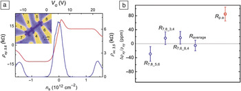
The first metrological results were obtained in 2008 by a Dutch collaboration, including the High Field Magnet Laboratory in Nijmegen and NMi Van Swinden Laboratory in Delft, using a small, 1-μm-wide Hall bar made of exfoliated monolayer graphene on Si/SiO2 that was provided by the Manchester group.Reference Giesbers, Rietveld, Houtzager, Zeitler, Yang, Novoselov, Geim and Maan17 The R H quantization was measured at 14 T and 350 mK on the plateaus at ν = –2 (hole density ≈ 7.8 × 1011 cm–2) and ν = +2 (electrons with the same density) by comparison with the quantized Hall resistance in a GaAs sample using a CCC. The reported R H value agreed with the expected value R K/2 within the experimental uncertainty of 15 × 10–6 (Figure 3). This large uncertainty was mainly explained by the high contact resistance (typically 1 kΩ) of the gold electrodes connected to the graphene, which caused noise across the voltage contacts and prevented the use of high measurement current without local heating of the carriers. Indeed, the characteristic critical current, the so-called “breakdown current”, above which Rxx increases exponentially above zero and R Hstrongly deviates from the expected quantized value, was low, about 3 μA, corresponding to a current density of 3 A/m.
Results from the first metrological study of the quantum Hall effect (QHE) in exfoliated monolayer graphene transferred onto Si/SiO2.Reference Giesbers, Rietveld, Houtzager, Zeitler, Yang, Novoselov, Geim and Maan17 (a) Transverse (Hall) resistivity (red) and longitudinal resistivity (blue) as functions of carrier density n s, controlled by gate voltage V G, at B = 14 T and T = 350 mK. (The resistivities ρ are related to the corresponding resistances by a dimensionless geometrical factor equal to unity in the case of the transverse [Hall] resistivity.) The plateaus at ν = –2 (with holes) and ν = 2 (with electrons) are clearly visible. Inset: a small sample with a carrier mobility of μ = 8000 cm2 V–1 s–1. (b) Relative deviation of the Hall resistivity (or resistance) from the expected value R K/2 measured on the plateaus at ν = ±2 by means of a cryogenic current comparator (CCC) with I = 1.5 μA using different contact configurations. R average is an average of the three other values represented by blue circles. The red square represents the deviation for a poorly annealed sample (R p.a.). The large uncertainty is caused by high-resistance contacts. Notation: Rij ,kl = (Vk – Vl)/Ii →j, where Vk is the potential at contact k and Ii →j is the current flowing between contacts i and j. 1 ppm (part per million) corresponds to 10–6. Reproduced with permission from Reference Reference Giesbers, Rietveld, Houtzager, Zeitler, Yang, Novoselov, Geim and Maan17. ©2008, American Institute of Physics.

It has been experimentally demonstratedReference Jeckelmann, Jeanneret and Inglis18 in GaAs Hall bars that a 10–9 accuracy of R H quantization requires contacts with a resistance below ∼10 Ω. Increasing the size of the graphene Hall bars should produce lower-resistance contacts simply by enabling an increase in their size. Moreover, as also observed in GaAs devices,Reference Jeckelmann, Rufenacht, Jeanneret, Overney, von Campenhausen and Hein19 increasing the width of the active channel directly results in an increase of the breakdown current.
Thus, the work by the Dutch group demonstrates the severe limitation of graphene produced by exfoliation of graphite with adhesive tape: the generally observed small size of the samples.
It is also worth noting that the most accurate quantization and highest QHE breakdown currents were measured after annealing of the sample at 380 K, which increased the carrier mobility at low temperature from 5000 cm2 V–1 s–1 to 8000 cm2 V–1 s–1. This points to surface dopants and, more generally, dopants in close proximity to graphene that can be removed by annealing as another possible source of limitations to QHE quantization accuracy.
At the Laboratoire National de Métrologie et d’Essais (LNE), the French NMI in Trappes near Paris, the metrological study of the QHE in graphene started in 2007, in collaboration with Service de Physique de l’Etat Condensé (SPEC)/Commissariat a l’Energie Atomique (CEA) (Gif sur Yvette, France). The first intention was to develop Hall bars from exfoliated graphene with properties fulfilling the metrological requirements for high-precision QHE quantization measurements, with flakes as large as possible and well-defined lateral metallic voltage contacts, away from the main channel, with resistance as low as possible. A Si/SiO2 substrate was chosen because its optical properties allow deposited graphene to be located easily by optical microscopy and also because it can act as an electrostatic back gate providing control of the carrier density in graphene by the field effect. Transport measurements were carried out in a 2 × 15 μm2 Hall bar based on monolayer (ML) graphene with palladium contacts and a 4.6 × 26 μm2bar based on bilayer (BL) graphene with titanium/gold contacts, both covered with a polymer resist [poly(methyl methacrylate)] to avoid contamination.Reference Guignard, Leprat, Glattli, Schopfer and Poirier20
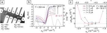
At low temperature (<1.5 K), ML and BL graphene showed moderate carrier mobilities of ∼4000 cm2 V–1 s–1 and ∼2300 cm2 V–1 s–1, respectively, after being annealed at ∼400 K under vacuum. In the QHE regime, in a high magnetic field (11.7 T for ML and 18.5 T for BL), contact resistances generally showed low values, from a few ohms to hundreds of ohms (although one value was as high as 6 kΩ). Accurate measurements of R H were performed, by comparison with a 100-Ω resistor calibrated with a GaAs quantum resistance standard and using a CCC, on the plateaus at ν = 2 (electron density ≈ 6.4 × 1011 cm–2) in the ML and at ν = –4 (hole density ≈ 2 × 1012 cm–2) in the BL. As shown in Figure 4c, the Hall resistance plateau measured in the BL near ν = –4, at 18.5 T and 350 mK and with a measurement current of 1 μA, was flat within 2 × 10⁻⁶ over a 3.5 × 1011 cm–2 density range. These measurements were complemented by accurate measurements of Rxx showing values of about 10 mΩ, which allowed a direct assessment of the dissipation. When extrapolated to zero dissipation (not shown), R H at the center of the plateau agreed with the expected value R K/2 in the ML and R K/4 in the BL within uncertainties of better than 5 × 10⁻⁷.
Results from the metrological study of the QHE in exfoliated bilayer graphene transferred onto Si/SiO2 at Laboratoire National de Métrologie et d’Essais (LNE).Reference Guignard, Leprat, Glattli, Schopfer and Poirier20 (a) Sample with low-temperature mobility of 2300 cm2 V–1 s–1 and low contact resistance in the QHE regime (18.5 T, 350 mK). (b) Hall resistance (R H) as a function of the carrier density, n s, at several magnetic fields and longitudinal resistivity (Rxx) (gray) at 18.5 T, both at 350 mK. (c) Relative deviation of the Hall resistance in the bilayer (BL) from the expected value of R K/4 realized in a GaAs Hall bar, ΔR H/R H = [2|R H,BL(ν = –4)| – R H,GaAs(ν = 2)]/R H,GaAs(ν = 2), as a function of the LL filling factor ν (and carrier density) around ν = –4 (holes) at several measurement currents at 350 mK and 18.5 T. One can also report ΔR H/R H as a function of Rxx with both measured for different current values (figure not shown). From the extrapolation of ΔR H/R H to zero dissipation state (Rxx = 0), it has been shown that, at hole densities of –2.0 × 1012 cm–2 and –2.1 × 1012 cm–2,R H in BL graphene agrees with R K/4 to within 5 × 10⁻⁷. Reproduced with permission from Reference Reference Guignard, Leprat, Glattli, Schopfer and Poirier20. ©2012, American Physical Society.

This accuracy of quantization was better than that observed in the earlier experiments but far from the target of 10–9. It appears that it was mainly limited by the remarkably low value of QHE breakdown currents (∼1 μA, corresponding to a current density of 0.25–0.5 A/m depending on the sample considered). Higher breakdown currents would have allowed the use of higher R Hmeasurement currents.
Detailed investigations were carried out to understand this limitation. The charge-carrier-density dependence of the conductivityReference Sarma, Adam, Hwang and Rossi21 and the quantum corrections to conductance that have been investigated in the BL (weak localizationReference Kedchedzi, Fal’ko, McCann and Altshuler22 and universal conductance fluctuations) at low magnetic field revealed that transport properties in the devices were mainly governed by the Coulomb interaction of carriers with a large concentration of charged impurities, specifically 2 × 1012 cm–2, 1 nm from the graphene, mainly in the SiO2 substrate and probably also in the PMMA layer on top of the graphene device. Contamination of amorphous SiO2by such impurities during its growth has already been reported.Reference Mc Caughan and Murphy23
These impurities impede mobility and create strong bipolar spatial fluctuations of carrier density with large amplitude (2.7 × 1011 cm–2 in the ML, 2.2 × 1012 cm–2 in the BL) and short typical correlation lengths (32 nm in the ML, 11 nm in the BL). These fluctuations explain the existence of the well-known “puddles” of spatially segregated electrons and holes at low carrier density. For the high carrier density fluctuations observed, such puddles can also persist far from the charge-neutrality point and favor the coexistence of the two carrier types (electrons and holes) at finite carrier density. Distinctive experimental signatures suggestive of puddles are seen in the BL up to a hole density of 2 × 1012 cm–2.Reference Guignard, Leprat, Glattli, Schopfer and Poirier20 In the QHE regime, the current dependence of the longitudinal conductivity was thoroughly investigated in the BL around ν = –4, showing that dissipation occurred through quasi-elastic inter-Landau-level scatteringReference Chaubet and Geniet24 assisted by an electric field. The enhanced scattering was ascribed to nearby charged impurities, acting both directly and by inducing strong fluctuations of the filling factor that lead to large local electric fields. The impact of such inhomogeneity was probably enhanced in the narrow exfoliated graphene samples studied, leading to the measured low breakdown current.Reference Guignard, Leprat, Glattli, Schopfer and Poirier20 This work highlighted the negative effect of charged impurities on QHE quantization in graphene and, more generally, the impact of the substrate supporting graphene on its transport properties. This is a consequence of the high sensitivity of monolayers of carbon atoms to their chemical environment.
As an alternative to using a Si/SiO2 substrate, important work was carried out at Physikalisch-Technische Bundesanstalt (PTB), the German NMI in Braunschweig, to develop a metrological QHE device based on exfoliated graphene deposited on GaAs.Reference Friedemann, Pierz, Stosch and Ahlers25 GaAs offers a smoother surface, and its higher dielectric constant (11.2 versus 3.9 for SiO2) provides better screening of charged impurities. Thus, with a GaAs substrate, a reduction of short-range (ripples) and long-range Coulombic scattering of graphene charge carriers was expected, which should yield graphene with better transport properties.
A specially tailored GaAs/AlAs multilayerReference Friedemann, Pierz, Stosch and Ahlers25 was grown by molecular beam epitaxy, which was designed to make graphene visible by optical contrast, as on Si/SiO2. The substrate also included a buried doped-GaAs layer, allowing it to be used as an electrostatic back gate to tune the carrier density. Monolayer graphene flakes exfoliated on these substrates were very large in area (40 × 175 μm2). The authors speculated that the hydrophilic character of GaAs could explain the larger sizes obtained than for Si/SiO2substrates.
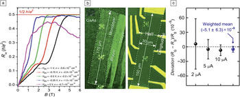
A first series of experimentsReference Woszczyna, Friedemann, Pierz, Weimann and Ahlers26 was carried out on a small, micrometer-wide Hall bar fabricated from such graphene flakes, with a carrier mobility of 11,000 cm2 V–1 s–1 at low temperature. The authors concluded that transport in both low and high magnetic fields, including in the QHE regime, was impacted by charged impurities (with a density of ∼9 × 1011 cm–2) in the close vicinity of graphene. Notably, at 50 mK, decreasing the carrier density to ∼3 × 1011 cm–2 destroyed the flatness of the ν = –2 Hall resistance plateau (appearing at a correspondingly reduced magnetic field of <6 T). The plateau actually exhibited reproducible distortions, and the value of the Hall resistance deviated from the expected value (Figure 5a).
Results from the metrological study of the QHE in exfoliated monolayer graphene transferred onto GaAs/AlAs.Reference Woszczyna, Friedemann, Pierz, Weimann and Ahlers26 (a) Hall resistance as a function of the magnetic field in a small micrometer-wide Hall bar with a mobility of 11,000 cm2 V–1 s–1 at 50 mK and several hole densities (defined as the negative of the electron density n s and varied by applying a back-gate voltage, V BG, between the graphene and the substrate). At high density, the ν = –6 and ν = –2 plateaus are clearly visible. When the density is decreased, the Hall resistance strongly deviates from the quantized value. This deviation is attributed to the formation of electron–hole puddles induced by charged impurities. Part (a) reproduced with permission from Reference Reference Woszczyna, Friedemann, Pierz, Weimann and Ahlers26. ©2011, American Institute of Physics. (b) Large Hall bar fabricated from monolayer graphene with low-resistance contacts (10 Ω) and a carrier mobility of 3000 cm2 V–1 s–1. (c) High-precision measurements using a CCCReference Woszczyna, Friedemann, Götz, Pesel, Pierz, Weimann and Ahlers28 of the relative deviation of the Hall resistance, R G, in this device from that in a GaAs sample, R S, on the plateau at ν = –2 (holes), at 18 T and 60 mK. The agreement with the expected value is within an uncertainty of 6.3 × 10⁻⁹. The QHE breakdown current is just above 10 μA. Parts (b) and (c) reproduced with permission from Reference Reference Woszczyna, Friedemann, Götz, Pesel, Pierz, Weimann and Ahlers28. ©2012, American Institute of Physics.

These deviations from quantization at low carrier density were attributed to the formation of electron and hole puddles, induced by charged impurities.Reference Poumirol, Escoffier, Kumar, Raquet and Goiran27 Contrary to expectations, the impact of charged impurities was not efficiently reduced by screening in this device. The authors suggested that these charged Coulombic impurities were in the GaAs substrate. However, such impurities could also possibly be adsorbed atoms on the graphene surface, as no high-temperature annealing was performed.
More generally, this work showed the possible difficulty in developing a graphene-based quantum resistance standard operating at low magnetic field. Although the Hall plateau at ν = ±2 is protected by the largest cyclotron gap, which gives much hope for the development of such a standard, measuring this plateau in a field of a few teslas requires reducing the carrier density to ∼1 × 1011 cm–2. At such low densities, it is difficult to avoid the formation of electron and hole puddles inherent to the ambipolar and gapless character of graphene.
Very recently, using a CCC, the PTB group measured the quantization of R H in a very large 30 × 150 μm2 Hall bar (Figure 5b) made of exfoliated monolayer graphene deposited on GaAs. On the ν = –2 plateau (with a hole density of ∼9 × 1011 cm–2), at 60 mK and 18 T, agreement with the expected value of R K/2 realized in a GaAs-based quantum resistance standard was found within an uncertainty of 6.3 × 10⁻⁹ (Figure 5c), approaching the target.Reference Woszczyna, Friedemann, Götz, Pesel, Pierz, Weimann and Ahlers28
The moderate mobility (3000 cm2 V–1 s–1), inhomogeneity of the carrier density, and low value of the breakdown current density (0.3 A/m, comparable to that found at LNE) suggest that transport was still limited by charged impurities in this case. The larger value of the breakdown current (10 μA), which explains the low measurement uncertainty, is due primarily to the large size of the device and secondarily to the resulting observed low value of contact resistance (10 Ω). This result also confirms the attenuation of the impact of charged-impurity-induced inhomogeneity by increasing the size of the device.
However, even if large sizes can occasionally be achieved in exfoliated graphene, there are serious doubts about the scalability and reproducibility of this production technique. Moreover, the limitation posed by charged impurities could be even more severe with less favorable quantization conditions (lower magnetic field, lower carrier density, higher temperature).
Quantum Hall effect in epitaxial graphene on SiC
The most convincing proof of principle that graphene can surpass GaAs as a quantum Hall resistance standard was shown using epitaxial graphene grown on silicon carbide (SiC).Reference Tzalenchuk, Lara-Avila, Kalaboukhov, Paolillo, Syvajarvi, Yakimova, Kazakova, Janssen, Fal’ko and Kubatkin29 In 2009, a consortium comprising National Physical Laboratory (NPL, the UK’s NMI) and Chalmers and Linköping Universities (both in Sweden) was among the first to observe the QHE in epitaxial graphene on SiC. This success resulted from better control of the growth process, namely, high-temperature annealing of 4H-SiC(0001) in an argon atmosphere, so that only one monolayer of graphene was grown on the silicon-terminated face (see also the article in this issue by Nyakiti et al.).
In a very large (35 × 160 μm2) Hall bar based on this monolayer graphene with low-resistivity titanium/gold contacts (<1.5 Ω), an electron density of 8.5 × 1011 cm–2, and a low-temperature mobility of ∼6000 cm2 V–1 s–1, perfect quantization of the Hall resistance was demonstrated within an uncertainty of 3 × 10⁻⁹, at the beginning of the plateau at ν = 2 at 300 mK.Reference Tzalenchuk, Lara-Avila, Kalaboukhov, Paolillo, Syvajarvi, Yakimova, Kazakova, Janssen, Fal’ko and Kubatkin29 Actually, the maximum available magnetic field of 14 T prevented observation of the entire plateau (Figure 6a–b).
Results from the metrological study of the QHE in epitaxial graphene on the silicon-terminated face of SiC.Reference Tzalenchuk, Lara-Avila, Kalaboukhov, Paolillo, Syvajarvi, Yakimova, Kazakova, Janssen, Fal’ko and Kubatkin29 (a) Atomic force microscopy image of a typical Hall bar fabricated from monolayer graphene grown at the surface. The Hall bar extends over several terraces. (b) Hall resistance Rxy (= R H) and longitudinal resistance Rxx as functions of magnetic field in a 35 × 160 μm2 Hall bar with low-resistivity contacts (<1.5 Ω), an electron density of 8.5 × 1011 cm–2, and a mobility of ∼6000 cm2 V–1 s–1, at 300 mK. ( $R_{xy}^{(0)} $ and
 $R_{xy}^{(1)} $ represent Hall resistance plateaus at filling factors ν = 2 and ν = 6, respectively.) At 14 T, the Hall resistance was foundReference Tzalenchuk, Lara-Avila, Kalaboukhov, Paolillo, Syvajarvi, Yakimova, Kazakova, Janssen, Fal’ko and Kubatkin29 to be quantized within an uncertainty of 3 × 10⁻⁹. Parts (a) and (b) reproduced with permission from Reference Reference Tzalenchuk, Lara-Avila, Kalaboukhov, Paolillo, Syvajarvi, Yakimova, Kazakova, Janssen, Fal’ko and Kubatkin29, courtesy of NPL. (c) Hall (red) and longitudinal (black) resistances as functions of magnetic field in the same device but with the electron density reduced to 4.6 × 1011 cm–2 and the mobility increased to ∼7500 cm2 V–1 s–1 by photochemical gating. At 1.5 K, the ν = 2 plateau (with electrons) is very broad because of pinning by charge transfer from the buffer layer. The QHE breakdown current, I c, reached a remarkably high value of 500 μA.Reference Janssen, Tzalenchuk, Yakimova, Kubatkin, Lara-Avila, Kopylov and Fal’ko31 Part (c) reproduced with permission from Reference Reference Janssen, Tzalenchuk, Yakimova, Kubatkin, Lara-Avila, Kopylov and Fal’ko31, courtesy of NPL. (d) Difference measured using a CCC-based resistance bridge between the Hall resistances quantized on the plateau at ν = 2 in a GaAs/AlGaAs sample (R S) and in the epitaxial graphene device (R G) as a function of the source–drain current (I SD) through the device for different measurement configurations. The graphene device is at 300 mK and 14 T. The weighted mean of all of the data points (red horizontal line) is –4.7 × 10⁻¹¹ with a standard uncertainty of 8.6 × 10⁻¹¹ (green horizontal lines). This result constitutes a relevant QHE universality test with a record uncertainty.Reference Janssen, Fletcher, Goebel, Williams, Tzalenchuk, Yakimova, Kubatkin, Lara-Avila and Falko33 The source–drain current is the same as the Hall-bar current I in other figures. Inset: Scanning electron microscopy image of the graphene device. Part (d) reproduced with permission from Reference Reference Janssen, Fletcher, Goebel, Williams, Tzalenchuk, Yakimova, Kubatkin, Lara-Avila and Falko33, courtesy of NPL.

By photochemically gating the device with active polymer resists,Reference Lara-Avila, Moth-Poulsen, Yakimova, Bjørnholm, Fal’ko, Tzalenchuk and Kubatkin30 the electron density was reduced to 4.6 × 1011 cm–2, and the mobility increased to ∼7500 cm2 V–1 s–1. This revealed the very broad extent of the Hall resistance plateau at ν = 2, reaching from 5 T to >14 T (when measured at T < 1.5 K and with a current of 1 μA). The remarkable width of the Hall resistance plateau is explained by the very large energy gap between the first and second graphene Landau levels involved in the quantization at ν = ±2 and also by a strong pinning of the filling factor at ν = 2.Reference Janssen, Tzalenchuk, Yakimova, Kubatkin, Lara-Avila, Kopylov and Fal’ko31 This pinning is a specific feature of the Si-face SiC epitaxial system. It results from the magnetic-field-dependent electron transfer into graphene from donor states in the buffer layer that forms on this face just before the growth of the graphene monolayer.
This pinning at ν = 2 could contribute to an enhancement of the QHE breakdown currents, measured up to 500 μA (corresponding to a current density of 14.3 A/m) in this device at 14 T and 1.5 KReference Janssen, Tzalenchuk, Yakimova, Kubatkin, Lara-Avila, Kopylov and Fal’ko31 (Figure 6c). For comparison, in GaAs-based metrological Hall bars, QHE breakdown current densities are around 0.5–1 A/m at 10 T and 1.5 K. An alternative or complementary explanation for the very high breakdown currents observed in this graphene device could be the high energy loss rate recently demonstrated for hot Dirac fermions in graphene.Reference Baker, Alexander-Webber, Altebaeumer and Nicholas32 Rates at least 10 times higher than those in GaAs were measured. In the considered epitaxial graphene sample, the enhanced energy relaxation could result from the coupling of carriers to the acoustical phonons of the SiC substrate. The possibility to take advantage of the high energy loss rate in this sample could also result from a reduced impact of charged impurities, notably the absence of the electric-field-induced breakdown as observed at LNE.
The high breakdown currents in this epitaxial graphene device enabled very accurate measurements of the quantized Hall resistance on the plateau at ν = 2 (electrons), 14 T, and 300 mK by direct comparison with GaAs-based quantum resistance standards using a CCC (Figure 6d). These measurements led, by averaging, to a determination of the quantized Hall resistance in graphene on this plateau in agreement with the value in GaAs within a record uncertainty of 9 × 10–11.Reference Janssen, Fletcher, Goebel, Williams, Tzalenchuk, Yakimova, Kubatkin, Lara-Avila and Falko33 This constitutes a highly relevant QHE universality test.
With the same device, it was demonstrated that R H quantization was accurate within an uncertainty of <1 × 10⁻⁸ on the plateau at ν = 2, when the temperature was increased to 15 K at a constant magnetic field of 14 T (and a current of 60 μA) or when the magnetic field was decreased to 10 T at a constant temperature of 300 mK (and a current of 60 μA).Reference Janssen, Williams, Fletcher, Goebel, Tzalenchuk, Yakimova, Lara-Avila, Kubatkin and Fal’ko34 The limitation in increasing temperature (at constant B) is compatible with the empirical criterion observed in GaAs that R H quantization at 10–9 requires ΔE ≈ 80k BT. The limitation in decreasing magnetic field is probably related to the experimental impossibility of further decreasing the carrier density in the device. Nevertheless, it remains unclear whether there is a more intrinsic limitation in this device related to the quality of the material itself, such as carrier mobility, that prevents a well-quantized QHE at low magnetic field.
Quantum Hall effect in CVD graphene
Very recently, encouraging resultsReference Shen, Wu, Yu, Richter, Elmquist, Newell and Chen35 were obtained at the National Institute of Standards and Technology (NIST), the US NMI, in collaboration with Purdue University. A well-developed quantum Hall effect with R H plateaus at ν = ±2, ±6, and ±10 at 14 T and up to 110 K was observed in ultralarge (7000 × 7000 μm2) monolayer graphene films, grown by chemical vapor deposition (CVD) on copper and transferred to Si/SiO2. Nevertheless, even at 1.7 K, the accuracy of the Hall resistance on the plateaus at ν = ±2, measured in the van der Pauw cloverleaf geometry, was limited to 10–2 and the longitudinal resistivity remained nonzero (∼500 Ω). This result might arise from voids in the film and scattering by impurities (notably charged impurities with a density of 1.4 × 1012 cm–2) that limited the carrier mobility to 4000 cm2 V–1 s–1, at best.
Challenges in materializing the promises
So far, the results obtained by NMIs have shown that most theoretical expectations for metrology with graphene QHE can be realized. Although these works have provided a convincing proof of principle, they have also pointed out experimental limitations and open questions.
The most stringent tests of QHE universality and, even more so, the development of a more convenient and better quantum resistance standard rely on improvement of the layer size and intrinsic quality of graphene, as well as control of its interactions with the substrate and with its environment. This essentially means better mastery of the materials.
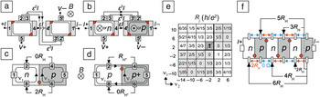
Large-size graphene is required for metrological applications, typically ≥6000 μm2, the largest areas in the previously described experiments, and preferably monolayer graphene for the development of a standard. The exfoliation technique is useful for testing and understanding QHE quantization, but epitaxial growth of graphene on SiCReference Berger, Song, Li, Li, Ogbazghi, Feng, Dai, Marchenkov, Conrad, First and de Heer36 and chemical vapor deposition (CVD) of grapheneReference Li, Cai, An, Kim, Nah, Yang, Piner, Velamakanni, Jung, Tutuc, Banerjee, Colombo and Ruoff37 are more suitable methods for meeting this objective. A graphene-based quantum standard will not be able to challenge GaAs-based standards until a well-controlled fabrication technique that can produce a large number of samples with reproducible properties to supply all NMIs becomes available. Moreover, large-size graphene layers are needed for the development of QHARS. Until now, their development with GaAs has relied on making multiple connections between a large number of single Hall bars. Although this techniqueReference Delahaye38 ensures overall accuracy by cancelling the quantization error induced by the resistive metallic link between Hall bars, it requires risky and low-yield technological processing over square-centimeter-sized surfaces. The ambipolarity of carriers in graphene could lead to a simplification of the connection scheme by exploiting the inversion of equipotential lines along sample edges by switching from hole doping (p) to electron doping (n) (Figure 7). In this way, series arrays could be simply fabricated from p–n junction arrays in graphene ribbons.Reference Woszczyna, Friedemann, Dziomba, Weimann and Ahlers39
Quantum Hall arrays in series. Triple series connection scheme of two Hall bars (a) in standard configuration and (b) for the case of opposite magnetic field or carrier type. (ε is the ratio of the resistance of the connection link to the resistance of a single Hall bar R H.) Note that, in (b), crossings of the wire leads can be avoided. Areas of high current density (“hot spots”) are marked at device corners; lines within the Hall bars denote equipotential lines. (c–d) Directly connected Hall bars with (c) bipolar filling factors ν1 and ν2 and (d) unipolar but unequal filling factors ν1 and ν2. In (c) and (d), lines denote the edge states that carry the current in the quantum Hall state, not equipotential lines. (e) Theoretical resistance values Rj expressed in units of h/e 2 calculated for filling factor pairs (ν1,ν2) between (c) terminal pair (6,8) and (d) terminal pair (2,4). (f) Schematic diagram of a graphene p–n junction series array.Reference Woszczyna, Friedemann, Dziomba, Weimann and Ahlers39 Reproduced with permission from Reference Reference Woszczyna, Friedemann, Dziomba, Weimann and Ahlers39. ©2011, American Institute of Physics.

Achieving perfect R H quantization at low magnetic field remains challenging and highly demanding. Until now, it has not been demonstrated at B < 10 T, far from the 1-T target for transportable systems, for instance. Limitations already observed at higher B could become far more severe.
Quantization at low B relies on graphene having a low carrier density. For example, the ambition to use the Hall plateau at ν = 2, which is protected by the largest cyclotron gap in monolayer graphene, at 1 T implies the reduction of the carrier density to ∼5 × 1010 cm–2. It is extremely challenging to reach such a low carrier density in graphene, all the more so because the density must remain very homogeneous to preserve quantization. At such a density, close to the Dirac point, it is difficult to avoid the formation of the electron–hole puddles inherent to the ambipolar and gapless character of graphene. In this context, control of the interaction of the graphene layer with the substrate, control of its surface contamination, and control of the defects in graphene itself are crucial issues. As an alternative, one can consider using the ν = 6 plateau at higher B (e.g., 3 T), so that the LL gap protecting the ν = 6 plateau becomes comparable to that protecting the ν = 2 plateau at 1 T (Figure 2b). This would raise the required density to ∼5 × 1011 cm–2. Control of the density of carriers and even of their sign is also required for devices based on ambipolarity, such as graphene QHARS.
Other considerations are also important for achieving R H quantization at low B. In terms of the targeted operating temperature (T ≈ 5 K), achieving the R H quantization criterion ΔE(B) ≫ k BT should not be a problem in monolayer graphene at ν = 2, even at 1 T. However, it might also be necessary to meet the empirical criterion for accurate R H quantization that μB ≫ 1. This criterion simply expresses that the level of disorder in the 2DEG has to be low enough that the cyclotron motion can be quantized: The charge carrier must complete a few cyclotron orbits before being scattered. Until now, metrological investigations have been based on graphene samples having moderate or low carrier mobilities at low temperature (<10,000 cm2 V–1 s–1) compared to the record value in suspended grapheneReference Du, Skachko, Duerr, Luican and Andrei40 (>260,000 cm2 V–1 s–1). Nevertheless, to satisfy the criterion μB ≫ 1, mobility much greater than 10,000 cm2 V–1 s–1 is required at 1 T. In the previously described graphene experiments at higher fields, R H quantization accuracy on the order of 10–9 was reported for μB ≥ 6, confirming that the accurate quantization criterion μB ≫ 1 probably makes sense in graphene. Investigations of R H quantization accuracy at μB ≈ 1, which are difficult to perform in high-mobility GaAs 2DEGs, might be useful to confirm this criterion. Regardless, to take full advantage of the properties of graphene, a high-mobility material is recommended, as well as control of defects, impurities, and the substrate.
Charged impurities are already known to reduce mobility because of their long-range scattering potential. They also prevent homogeneous and low carrier densities from being obtained, because they induce fluctuations in the carrier density and formation of electron–hole puddles with densities on the order of 1011 cm–2, as generally observed in graphene on SiO2. Other scatterers could also disrupt higher-precision quantization, including ripples and vacancies or intrinsic defects. Generally, to limit possible chemical surface contamination of graphene, encapsulation should be considered. Extrinsic impurities are also critical for graphene transferred onto an insulating substrate, such as exfoliated graphene and CVD graphene. In this case, the choice of the substrate must be made judiciously. Hexagonal boron nitride (h-BN) is probably a much better substrate than SiO2. High electron mobilities (80,000 cm2 V–1 s–1) have been obtained in exfoliated graphene deposited on h-BN.Reference Dean, Young, Meric, Lee, Wang, Sorgenfrei, Watanabe, Taniguchi, Kim, Shepard and Hone41 Indeed, the combination of h-BN with large-size CVD graphene is especially promising for the considered metrological application. In the case of CVD graphene, the effect of grain boundaries between crystallites, which are inescapable in large samples (>50 μm), must be investigated.
Epitaxial graphene grown on SiC by silicon sublimation is also very promising, as demonstrated by the initial metrological results described previously. When grown on the silicon-terminated face, graphene is strongly coupled to SiC through a buffer layer, which allows electron transfer in graphene. This is an advantage because it pins the ν = 2 quantum Hall state. However, this coupling also pins the Fermi level at zero magnetic field, leading to a high electron doping level of ∼1013 cm–2 and a moderate mobility of ∼5000 cm2 V–1 s–1, as generally observed. This pinning is problematic for the earlier-described metrological applications that require reducing the carrier density, changing the carrier type from electrons to holes, or achieving higher mobility. For example, although perfect quantization of R H has been demonstrated for electrons in epitaxial graphene, it will also be interesting to investigate R Hquantization for holes, whose density is not pinned, in contrast to that of electrons. In addition, for the metrological application of the QHE at frequencies in the kilohertz range, desirable for a quantum impedance standard, the strong capacitive coupling of the graphene layer with the buffer layer might be a problem.
Technological solutions must be envisaged to adjust the carrier density in epitaxial graphene grown on SiC, especially on the Si face, such as gating;Reference Lara-Avila, Moth-Poulsen, Yakimova, Bjørnholm, Fal’ko, Tzalenchuk and Kubatkin30, Reference Waldmann, Jobst, Speck, Seyller, Krieger and Weber42, Reference Jouault, Camara, Jabakhanji, Caboni, Consejo, Godignon, Maude and Camassel43 doping compensation, by oxygen adsorption,Reference Pallecchi, Ridene, Kazazis, Mathieu, Schopfer, Poirier, Mailly and Ouerghi44 for example; or decoupling from the substrate, at least partially, by hydrogenation,Reference Riedl, Coletti, Iwasaki, Zakharov and Starke45 for example. Open questions remain regarding the homogeneity of the carrier density if it is successfully reduced, the existence and screening of charged impurities, and the formation of electron–hole puddles.
Expectations are also high for graphene grown on the carbon-terminated face of SiC, because strong coupling to the substrate through a buffer layer does not exist for growth on this face. In fact, a carrier mobility of 20,000 cm2 V–1 s–1has been achieved for C-face epitaxial graphene.Reference Wu, Hu, Ruan, Madiomanana, Hankinson, Sprinkle, Berger and de Heer46
Measurements of conductivity and its quantum corrections are useful tools for understanding the mechanisms that determine both the electron mobility and the carrier concentration in CVD and epitaxial graphene,Reference Guignard, Leprat, Glattli, Schopfer and Poirier20, Reference Lara-Avila, Tzalenchuk, Kubatkin, Yakimova, Janssen, Cedergren, Bergsten and Fal’ko47 because these effects depend on microscopic details of elastic scattering (e.g., inter- and intravalley scattering). They can be advantageously combined with structural and electronic band structure characterizations (e.g., angle-resolved photoemission spectroscopy, scanning tunneling spectroscopy, Raman spectroscopy, atomic force microscopy).
Fundamental tests of QHE universality do not demand the same ease of implementation as widely used standards. Still, these tests will benefit from all of the progress in mastering graphene that is envisaged for the development of an improved graphene-based quantum resistance standard. The objective is to reduce the uncertainty in universality to 10–12using the original quantum Wheatstone bridge technique developed at LNE.Reference Schopfer and Poirier48
Conclusions
Several national metrology institutes (NMIs) are now involved in graphene metrology research. Many are focusing their efforts on developing resistance and impedance standards, but some laboratories are already interested in other applications, such as gas detectors or terahertz detectors. The metrological approach performed at the limits of instrumentation can complete the understanding of graphene physics. Moreover, meeting the highly demanding metrological requirements for application of the graphene quantum Hall effect (QHE) (quality of electrical contacts, control of electronic properties such as mobility and density over large millimeter-sized areas) further enhances the severity of the benchmark test offered by the QHE for the quality of any two-dimensional material. This makes the metrological study of the graphene QHE highly significant and useful for the development of materials and also for industrial applications such as microelectronics.
Acknowledgments
The authors thank D.C. Glattli, notably for collaboration on exfoliated graphene, and J. Guignard for his work on graphene as a PhD student at LNE. The work by the authors toward the application of the quantum Hall effect in graphene to metrology is supported by Grant ANR-2011-P2N-004-METROGRAPH from the French National Research Agency, Project GAMET from the French RTRA “Triangle de la Physique”, and the Partner University Fund from the Embassy of France in the United States.