Introduction
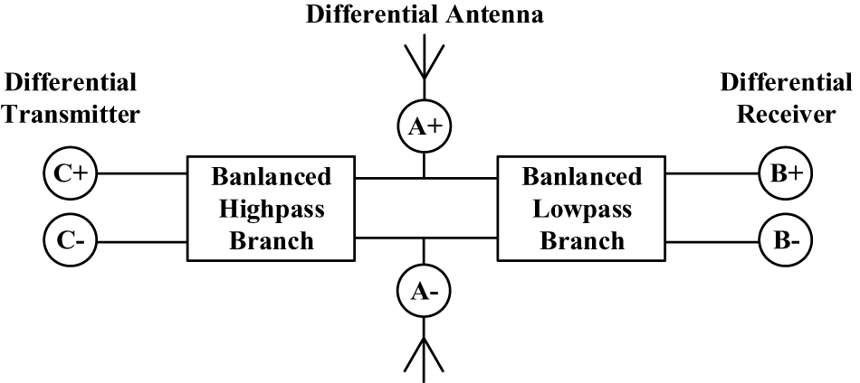
Diplexers are essential passive components in microwave systems, which can work together with antennas to transmit and receive required signals [Reference Yang, Chi and Itoh1–Reference Zhang, Wong, Lin, Liu, Zhu and He3]. However, with the rapid advancements in wireless communication systems, diplexers are now needed to meet more rigorous requirements. Traditionally, the widely adopted approach involves connecting two bandpass filters with different center frequencies using a T-junction [Reference Xiao, Zhu, Li, Tian and Ma4, Reference Xue, Yang, Xu, Zhao and Zhang5]. But this method necessitates additional matching circuits, resulting in an oversized circuit size. Therefore, researchers have explored alternative designs to reduce circuit size; many diplexers with compact sizes were published in refs [Reference Chen, Tseng, Su, Li, Wang and Li6–Reference Xu, Zhan, Li and Zhang9]. But their inter-channel isolation is poor. To address this issue, the isolation is improved while realizing a compact structure by sharing a resonator as the filtering structure and feeding network to increase the out-of-band transmission zeros in refs [Reference Chuang and Wu10–Reference Xiao, Zhang and Ma12]. However, the above diplexers are single-ended structures and cannot provide high immunity to electromagnetic interference and noise [Reference Gómez-García, Yang and Munoz-Ferreras13, Reference Song, Yao, Chen, Zhou, Zhu and Fan14]. Therefore, many unbalanced-to-balanced diplexers have been proposed [Reference Chen, Chang, Yang and Chen15–Reference Tian, Liu, Zheng and Zuo17], but this design is not suitable for use in systems with differential antennas and is insufficient to cope with the complex and variable noise environment [Reference Zhou, Deng and Zhao18]. As shown in Fig. 1, balanced-to-balanced diplexers are particularly important in high-density communication environments as critical interface devices between differential antennas and differential transceivers in the radio-frequency (RF) front end [Reference Wei, Liu, Wang and Zhao19, Reference Zhao, Wang, Gao, Liu and Fang20]. In recent years, balanced-to-balanced diplexer designs utilizing symmetrical resonators or microstrip-to-slotline transition structures have been published in refs [Reference Zhang, Zhu and Li21–Reference Wei, Cheng, Liu and Shi24]. However, the balanced-to-balanced diplexer in Zhang et al. [Reference Zhang, Zhu and Li21] has insufficient in-band common-mode (CM) noise suppression (only 23 dB). Besides, the 20-dB bandwidths of differential-mode (DM) stopband [Reference Song, Wen, Liu, Wang and Geng22–Reference Wei, Cheng, Liu and Shi24] and out-of-band CM noise suppression [Reference Song, Wen, Liu, Wang and Geng22, Reference Fernández-Prieto, Lujambio, Martín, Martel, Medina and Boix23] are narrow. Accordingly, the harmonics are made to move away from the passband by exploiting the harmonic characteristics of the resonator [Reference Deng, Zhang, Liu, Xu and Chen25–Reference Fernández-Prieto, Lujambio, Martel, Medina, Martín and Boix27], thus broadening 20-dB bandwidths of the DM stopband and the CM noise suppression. But the bandwidths of the DM stopband and the CM noise suppression broadened in this way are often limited by the structure of resonators and cannot realize a more excellent wide DM stopband response and a wideband CM noise suppression response.
The structure of the RF front-end with a balanced-to-balanced diplexer.

To overcome these issues, this paper has proposed a novel planar balanced-to-balanced diplexer with high isolation and harmonic suppression, which is designed and fabricated on the F4B substrate with h = 1.0 mm, εr = 2.6, and tanδ = 0.003. The filtering structure of the proposed diplexer comprises two-stepped impedance resonators (SIRs) and one uniform impedance resonator (UIR). The differential feed ports symmetrically excite the SIR for CM suppression and DM transmission. In order to enhance the inter-channel isolation of the diplexer, the cross-coupling between the SIRs is used to introduce the extra out-of-band transmission zeros. At the same time, the harmonic characteristics of SIRs with different impedance ratios are utilized so that the harmonics of each channel are suppressed by the asymmetric configuration of SIRs, which cannot form an effective spurious passband, thereby broadening the DM stopband and enhancing the out-of-band CM suppression. Specifically, the contribution of this work can be summarized as follows: (i) excellent harmonic suppression (wide DM stopband and wideband CM suppression), (ii) excellent DM isolation, and (iii) great design flexibility. The detailed design methodology is described as follows.
Diplexer structure and analysis
Characteristics of the SIR and UIR
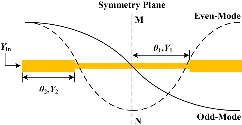
Based on the selected F4B substrate, this section begins by introducing the SIR and UIR. The structure of the SIR is depicted in Fig. 2, where θi and Yi (i = 1, 2) represent the electrical length and characteristic admittance of the microstrip line, respectively. According to transmission line theory, the input admittance of SIR is
 \begin{equation}{Y_{{\text{in}}}} = \frac{{2{\text{j}}{Y_2}({R_{\text{z}}}\tan {\theta _1} + \tan {\theta _2})({R_{\text{z}}} - \tan {\theta _1}\tan {\theta _2})}}{{{R_{\text{z}}}(1 \!- {{\tan }^2}\,{\theta _1})(1 \!- {{\tan }^2}\,{\theta _2}) - 2(1 - R_{\text{z}}^2)\tan{\theta _1}\tan {\theta _2}}}\end{equation}
where R z is the impedance ratio, R z = Y 1/Y 2. When R z = 1, it is UIR. When Y in = 0, the odd- and even-mode resonance conditions can be derived as
 \begin{equation}\tan\left[\left(1-a\right)\left(\theta_1+\theta_2\right)\right]\tan\left[\alpha\left(\theta_1+\theta_2\right)\right]=R_2\;\;\left(\mathrm{Odd}-\mathrm{mode}\right)\end{equation}
 \begin{equation}R_ztan\left[\left(1-\alpha\right)\left(\theta_1+\theta_2\right)\right]+\tan\left[a\left(\theta_1+\theta_2\right)\right]=0\;\;\left(\mathrm{Evee}-\mathrm{mode}\right)\end{equation}
The structure of the stepped impedance resonator.

where α is the electrical length ratio, α = θ 2/(θ 1 + θ 2). From Equations (2) and (3), it can be analyzed that for the SIR, both the odd- and even-mode resonance conditions are related to θi, α, and R z. As illustrated in Fig. 2, the solid and dashed lines indicate the voltage distribution of the SIR under odd- and even-mode excitation, respectively, and the symmetry plane MN behaves as a shorted circuit under odd-mode excitation and an opened circuit under even-mode excitation, which ensures that the dominant resonance is excited exclusively by the DM signal and effectively suppresses the CM noise.
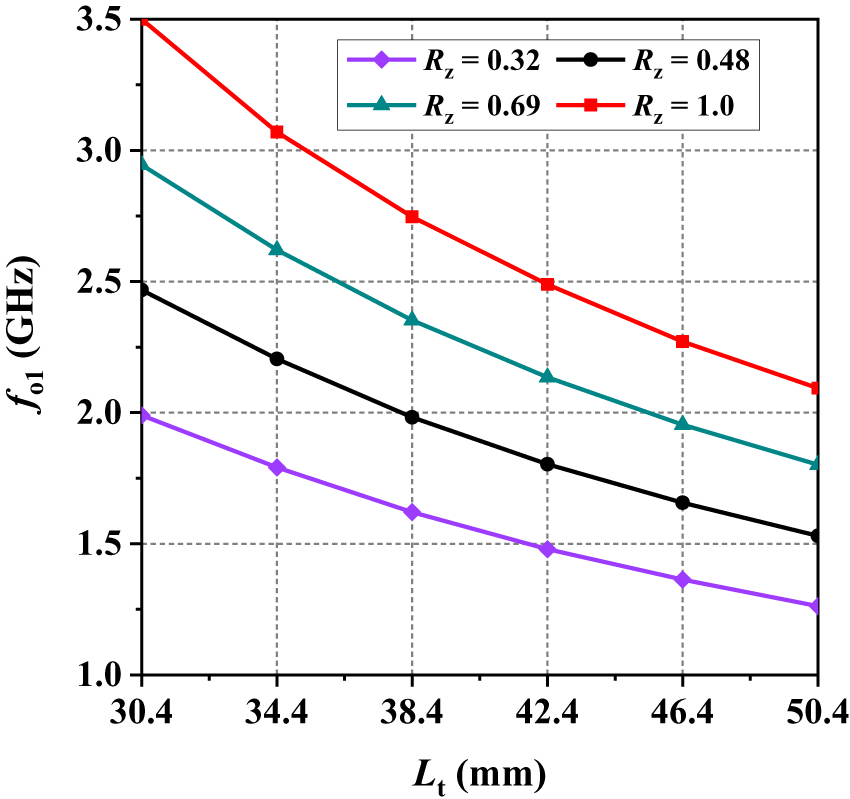
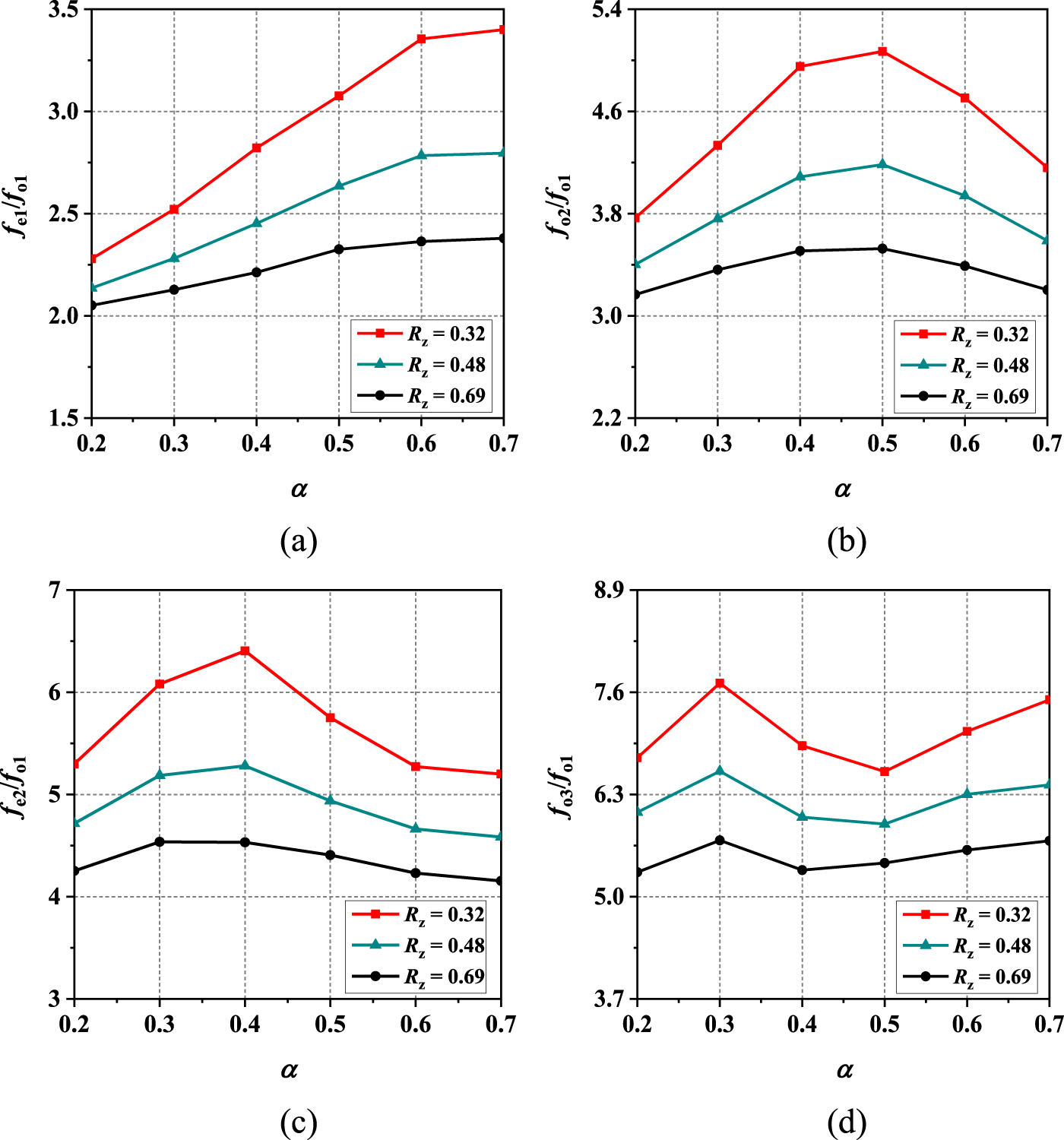
The SIR has an infinite number of resonant modes. The fundamental resonance occurs in the odd-mode, the second resonance in the even-mode, and higher-order resonances in that order. Here we discuss the first five resonance modes in detail. Figure 3 plots the variation of the f o1 (the first-order odd-mode resonant frequency of the SIR) with the physical dimension L t (L t is the total physical length corresponding to the electrical length 2θ 1 + 2θ 2) when R z is different. The results indicate that f o1 gradually decreases as L t increases, and when f o1 is identical, the overall physical dimension decreases as the R z decreases. Accordingly, the stepped impedance structure facilitates a compact design [Reference Chen, Tseng, Su, Li, Wang and Li6, Reference Roshani and Roshani7]. Figure 4 depicts the variation of the resonant frequencies ratio with α when R z is different; it suggests that when R z < 1, with the increase of α, the f e1/f o1 increases gradually, the f o2/f o1 and f e2/f o1 initially increase and then decrease, and the f o3/f o1 first increases, then decreases, and then increases again. Here, f e1 represents the first-order even-mode resonant frequency of the SIR, f o2 represents the second-order odd-mode resonant frequency of the SIR, f e2 represents the second-order even-mode resonant frequency of the SIR, and f o3 represents the third-order odd-mode resonant frequency of the SIR. And these high-order resonant frequencies increase as R z decreases, as shown in Fig. 4. That is to say, by adjusting the R z and α, the higher-order harmonics of SIRs can be positioned at different locations, which indicates that SIRs with different R z and α will contribute to achieving wide DM stopband and wideband CM suppression. Besides, this design does not require tuning the resonant frequency ratio to its maximum; it only needs to ensure that the spurious harmonics of the used resonators are as widely spaced as possible. Through experimental verification, from the point of view of suppressing spurious harmonics and achieving a compact layout, the R z of the SIRs are ultimately selected as 0.69 and 0.32 for the lower channel, and the R z of the SIRs are ultimately selected as 0.69 and 0.48 for the higher channel. To simplify the simulation, the α for SIR with R z = 0.69 is set to 0.51, while the α for R z = 0.32 and R z = 0.48 are both set to 0.43.
Curves of the variation of f o1 with the physical dimension L t (Y 1 = 0.0114 S).

Curves of the variation of the resonant frequencies ratio with the α (Y 1 = 0.0114 S). (a) f e1/f o1, (b) f o2/f o1, (c) f e2/f o1, (d) f o3/f o1.

Coupling routing scheme
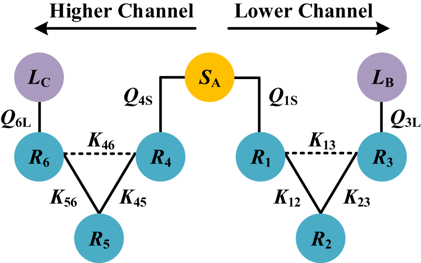
Figure 5 illustrates the coupling topology of the proposed balanced diplexer. In this topology, S and L represent the differential source and load, respectively; solid lines denote strong coupling, dashed lines denote weak coupling, R 1, R 3, R 4, and R 6 correspond to fundamental resonant modes of the SIRs, and R 2 and R 5 denote fundamental resonant modes of the UIRs. Their resonant frequencies are f R1, f R3, f R4, f R6, f R2, and f R5.
The coupling topology of the proposed balanced diplexer.

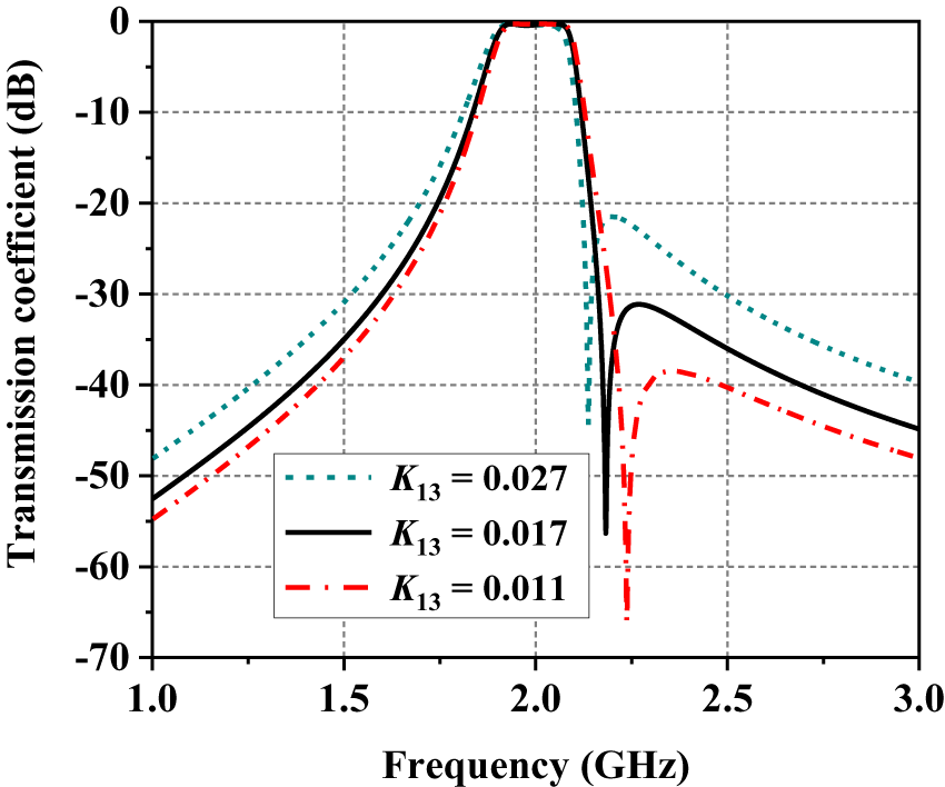
The lower channel is formed by coupling the three resonators R 1, R 2, and R 3, while the higher channel is established by coupling R 4, R 5, and R 6. Both channels exhibit a third-order bandpass response, enhancing channel selectivity. DM isolation between channels is improved by introducing out-of-band transmission zeros through cross-coupling between SIRs. And by adjusting K 13 and K 46, the transmission zeros can be controlled. Here, the control of the transmission zero of the lower channel is described as an example. The control mechanism of the transmission zero of the higher channel is similar to it. Figure 6 illustrates the curve of the transmission coefficients with the different values of K 13. It can be observed that as the coupling coefficient K 13 gradually increases, the transmission zero gradually moves closer to the passband, but the stopband suppression level deteriorates. Therefore, when adjusting the transmission zero, it is necessary to weigh the suppression level of the stopband, ultimately selecting an appropriate coupling coefficient K 13. It is also worth noting that the lower and higher channels each possess independent transmission paths, allowing for separate control over the center frequencies and bandwidths. This ensures that the design of the balanced diplexer has greater flexibility.
Curve of the transmission coefficients with the different K 13.

Design of the balanced-to-balanced diplexer
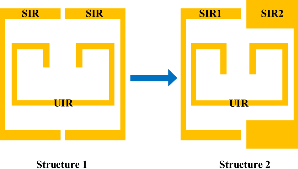
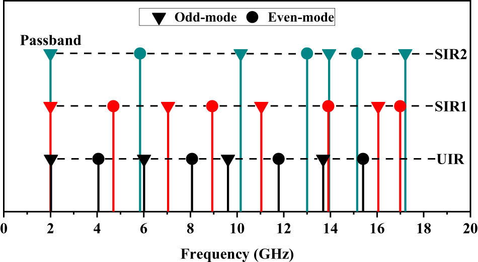
The evolution of the bandpass filtering structures is shown in Fig. 7. Both structures use cross-coupling to introduce additional transmission zeros. For structure 1 with a symmetric configuration of SIRs, although an upper stopband up to 3.5f 0 and CM suppression up to 2.3f 0 are achieved by adjusting the impedance ratio of the SIRs to keep their second-order odd-mode and first-order even-mode harmonics away from the fundamental resonance frequency f 0, they still affect the performance of the diplexer through the weak coupling path. For structure 2 with an asymmetric configuration of SIRs, in order to further broaden the upper stopband and CM suppression bandwidths, employ SIRs with different impedance ratios, such that the harmonics of the two SIRs and UIR are different from each other. When the passband center frequency is 2.0 GHz, the resonant-frequency spectra of SIR1, SIR2, and UIR are shown in Fig. 8, which shows that, except for the fundamental frequencies (i.e., first-order odd-mode resonances), the three resonators have different first-order even-mode harmonics, second-order odd-mode harmonics, second-order even-mode harmonics, third-order odd-mode harmonics, etc.
The evolution of the bandpass filtering structures.

The resonant-frequency spectra of SIRs and UIR.

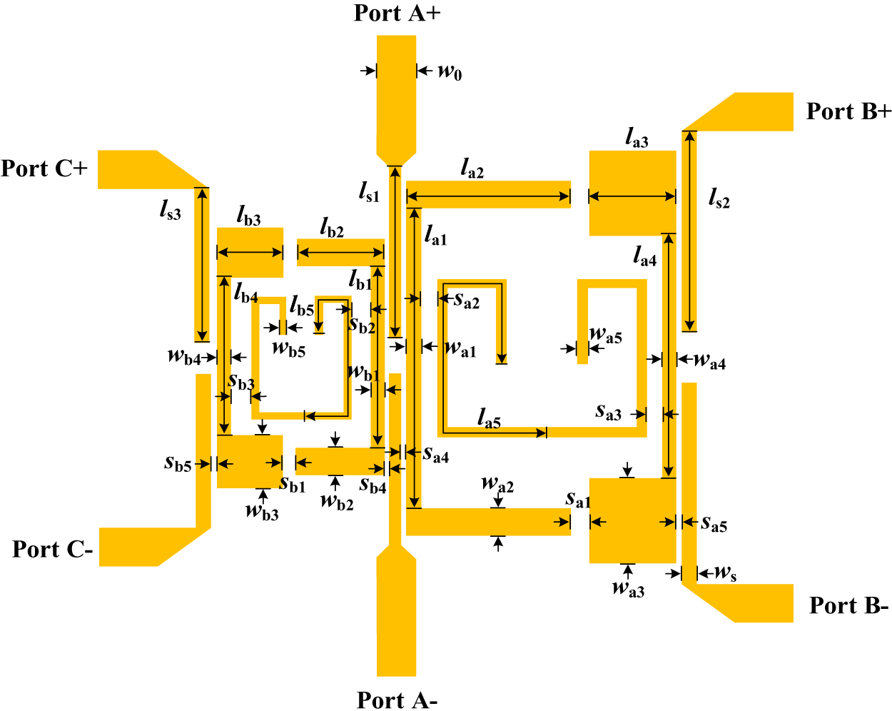
The balanced diplexer is designed with the layout shown in Fig. 9. Port A serves as the differential antenna port, while Ports B and C function as the differential transceiver port. The transmission coefficients between the differential ports can be defined by the mixed-mode S-parameters [Reference Eisenstant, Stengel and Thompson28]. For example, the DM and CM transmission coefficients between differential Port A and differential Port B can be defined as |S ddBA| and |S ccBA|, respectively, which represent the transmission responses between differential ports.
Layout of the proposed balanced diplexer.

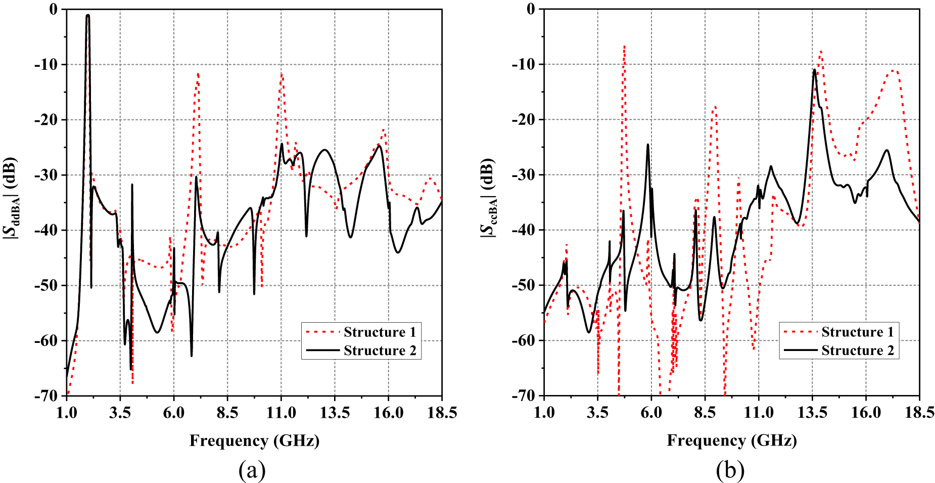
Compared to the parallel-coupled single-band and dual-band bandpass filters using the SIRs with different dimensions [Reference Kuo and Shih29, Reference Kuo and Lin30], the coupling topology and the input/output feed method of the filtering structures in this paper and the principle of harmonic suppression are different. The principle of harmonic suppression in Kuo and Lin [Reference Kuo and Lin30] is to collocate the transmission zeros generated by the tap feed method [Reference Kuo and Shih29] and inherent transmission zeros of open-circuited parallel-coupled lines [Reference Kuo and Lin30], but the principle of harmonic suppression in this paper is based on the excitation principle. Specifically, based on the layout and coupling topology of the proposed balanced diplexer shown in Fig. 9 and Fig. 5, due to the symmetrical feed ports exciting the SIRs, the even- and odd-mode harmonics of the SIRs only can be excited by common- and differential-modes, respectively; thus, the DM signal can pass only when the three resonators (SIR1, SIR2, and UIR) have the same odd-mode resonant frequency, and when the odd-mode resonant frequencies of the three resonators are different, especially when the odd-mode resonant frequencies of resonators R 1 and R 3 are different, the DM signal will be blocked to achieve a wide DM stopband. Similarly, when the even-mode resonant frequencies of resonators R 1 and R 3 are different, the CM noise will also be blocked to achieve wideband CM suppression. In this design, the three resonators have the same resonant frequency only at the fundamental frequency, while the even- and odd-mode spurious harmonics of the three resonators cannot resonate at the same frequency in the high-frequency band. Therefore, the proposed diplexer can result in wideband harmonic suppression. For example, between differential Port A and differential Port B, the comparison of the DM upper stopband (which can be expressed by |S ddBA|) and CM suppression (which can be expressed by |S ccBA|) simulation results for two different filtering structures is shown in Fig. 10.
The comparison of the stopband and CM suppression simulation results. (a) |S ddBA|, (b) |S ccBA|.

It can be seen from Fig. 10(a) that for the structure 1 (resonators R 1 and R 3 use the same SIR1, the second-order and third-order odd-mode harmonics of which resonate at about 7.1 GHz and 11 GHz, respectively, as shown in Fig. 8), the DM out-of-band suppression near 7.1 GHz and 11 GHz is only about 12 dB (i.e., |S ddBA| is about − 12 dB), but when resonators R 1 and R 3 use the different SIRs (i.e., the structure 2 with asymmetric configuration of SIRs), resonators R 1 and R 3 (i.e., SIR1 and SIR2) have different resonant frequencies of second-order and third-order odd-mode harmonics, the DM out-of-band suppression near 7.1 GHz and 11 GHz has been significantly enhanced, achieving a wide 20-dB DM stopband. It can be seen from Fig. 8 that the first-order and second-order even-mode harmonics of the SIR1 resonate at about 4.7 GHz and 9 GHz, respectively; thus, the CM suppression for the structure 1 near 4.7 GHz and 9 GHz is less than 20 dB (i.e., |S ccBA| > − 20 dB), as shown in Fig. 10(b). Similarly, by using an asymmetric configuration of SIRs, different even-mode resonant frequencies of SIR1 and SIR2 result in 20-dB CM suppression up to 13.4 GHz, achieving wideband CM suppression.
The design specifications for the lower channel of the balanced diplexer are as follows: The center frequency f L is 2.0 GHz with a 3-dB fractional bandwidth (FBW) of 7.5% and a return loss (RL) of 15 dB. The coupling matrix can be synthesized as
 \begin{equation}{{\mathbf{M}}_{\mathbf{L}}} = \left[ {\begin{array}{*{20}{c}}
0&{0.794}&0&0&0 \\
{0.794}&0&{0.647}&{0.227}&0 \\
0&{0.647}&{ - 0.285}&{0.720}&0 \\
0&{0.227}&{0.720}&0&{0.959} \\
0&0&0&{0.959}&0
\end{array}} \right]\end{equation}
The required coupling coefficients K 12, K 13, and K 23 and the lower channel loaded quality factors (Loaded-Q) Q 1S and Q 3L are calculated as [Reference Hong and Lancaster31]:
 \begin{equation}K_{12}=\text{FBW}\cdot m_{12},\,K_{13}=\text{FBW}\cdot m_{13},\;K_{23}=\text{FBW}\cdot m_{23}\end{equation}
 \begin{equation}Q_{1\text{S}}=\frac1{\text{FBW}\cdot m_\text{1S}^2},\;\,Q_{3\text{L}}=\frac1{\text{FBW}\cdot m_\text{3L}^2}\end{equation}
The required fundamental resonant frequency of the UIR is determined by the following equation [Reference Hong and Lancaster31]:
 \begin{equation}{f_{{\text{R}}2}} = {f_{\text{L}}} \cdot \left( {1 - \frac{{{m_{{\text{22}}}} \cdot {\text{FBW}}}}{2}} \right)\end{equation}
 \begin{equation}{{\mathbf{M}}_{\mathbf{H}}} = \left[ {\begin{array}{*{20}{c}}
0&{0.887}&0&0&0 \\
{0.887}&0&{0.650}&{0.350}&0 \\
0&{0.650}&{ - 0.445}&{0.625}&0 \\
0&{0.350}&{0.625}&0&{0.829} \\
0&0&0&{0.829}&0
\end{array}} \right]\end{equation}
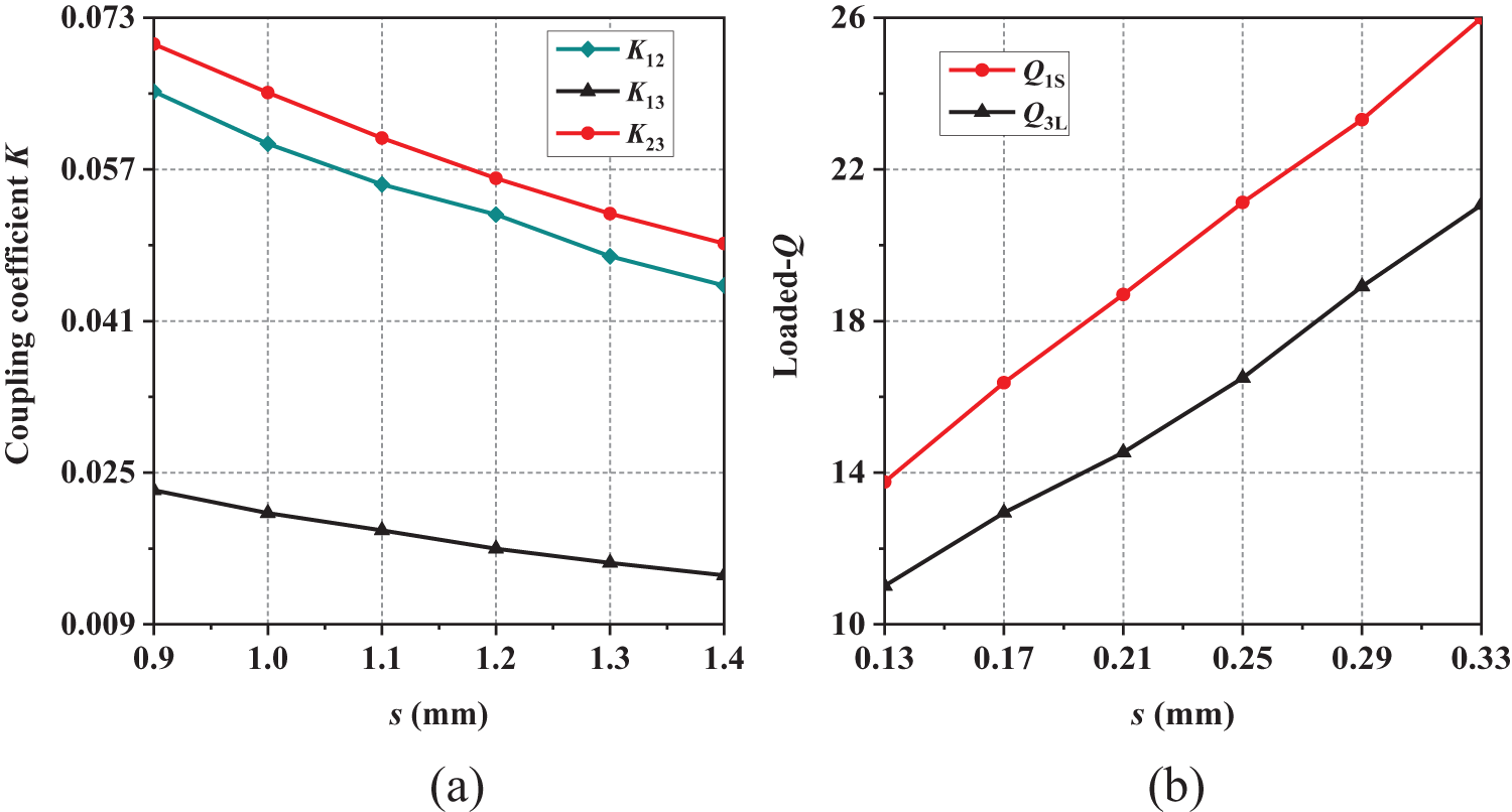
Based on Equations (5)–(7), the calculated parameters for the lower channel are K 12 = 0.0485, K 13 = 0.0170, K 23 = 0.0540, Q 1S = 21.15, Q 3L = 14.50, f R1 = f R3 = 2000.0 MHz, and f R2 = 2021.4 MHz. Figure 11(a) shows the curves of coupling coefficients K for the lower channel as the gap s changes. Figure 11(b) illustrates the curves of loaded-Q as the gap s changes. To meet the design specifications, the coupling coefficients K and the loaded-Q must match the calculated values. This can be achieved by carefully selecting the relevant physical dimensions, as indicated in Fig. 11, to satisfy the design requirements. And the resonant frequencies of the resonators are adjusted by tuning length.
The curves of coupling coefficients K and loaded-Q for the lower channel as the gap s changes. (a) Coupling coefficients K. (b) Loaded-Q.

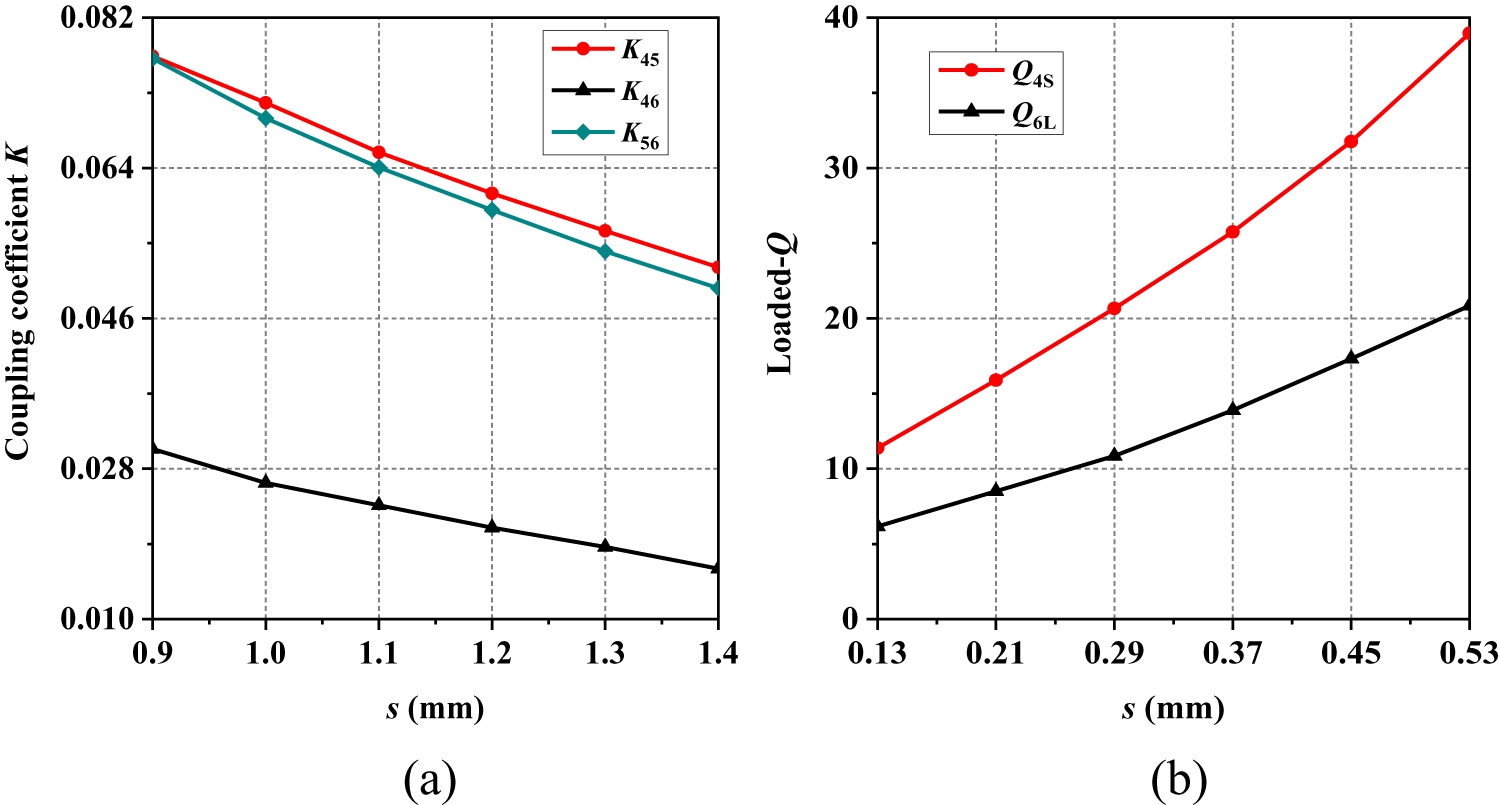
The center frequency f H, 3-dB FBW, and RL of the higher channel of the balanced diplexer are 3.5 GHz, 8.0%, and 15 dB, respectively, with the coupling matrix given by Equation (8). Similarly, the required coupling coefficients K, loaded-Q, and fundamental resonant frequencies are calculated as follows: K 45 = 0.0520, K 46 = 0.0280, K 56 = 0.0500, Q 4S = 15.89, Q 6L = 18.19, f R4 = f R6 = 3500.0 MHz, and f R5 = 3562.3 MHz. Figure 12(a) illustrates the curves of the higher channel coupling coefficients K as the gap s changes. Figure 12(b) shows the relationship between the higher channel loaded-Q and the gap s. By carefully selecting the relevant physical dimensions based on Fig. 12, the desired coupling coefficients K and loaded-Q can be achieved to meet the design specifications. And the self-resonant frequencies are adjusted by tuning length.
The curves of coupling coefficients K and loaded-Q for the higher channel as the gap s changes. (a) Coupling coefficients K. (b) Loaded-Q.

Design procedure
Based on the above analysis, the design procedure for the proposed novel planar balanced-to-balanced diplexer with high isolation and harmonic suppression can be summarized as follows:
Step 1: Define diplexer center frequencies, along with the 3-dB FBW and RL, and synthesize the coupling matrix.
Step 2: Using the synthesized coupling matrix, determine the center frequencies of the SIRs and the UIR, and employ eigenmode analysis in HFSS to select the appropriate impedance ratio for the SIRs and sequentially simulate the different gaps according to coupling coefficients K and the loaded-Q. Ensure that both channels exhibit great third-order filtering responses.
Step 3: Combine the two channel structures and perform simulations. Optimize the physical dimensions of the overall structure to address potential issues arising from the discontinuity and the interaction.
Experimental verification
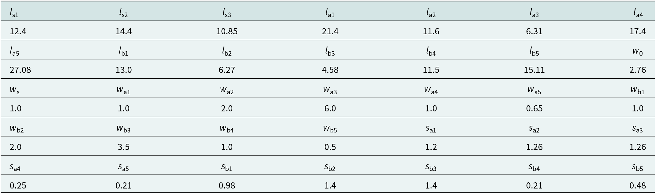
The proposed novel planar balanced-to-balanced diplexer, featuring high isolation and harmonic suppression, is designed and fabricated on the F4B substrate. A photograph of the fabricated prototype is shown in Fig. 13. The overall circuit size is 0.47λ g × 0.44λ g (48 mm × 45 mm), where λ g is the guided wavelength at f L. The optimized final physical dimensions of the proposed balanced diplexer are shown in Table 1 (unit: mm). The simulated and measured results are presented in Fig. 14. The various mixed S-parameters are defined as follows: |S ddAA| represents the reflection coefficients under DM excitation, |S ddBA| and |S ddCA| represent the transmission coefficients under DM excitation, |S ccBA| and |S ccCA| represent the transmission coefficients under CM excitation, |S ddBC| represents DM isolation, and |S ccBC| represents CM isolation.
The photograph of the fabricated prototype.

The simulated and measured mixed S-parameters. (a) Wideband DM frequency responses. (b) Details of the DM frequency response. (c) Wideband DM isolation and CM isolation. (d) Details of DM isolation and CM isolation. (e) Wideband CM frequency responses. (f) Details of the CM frequency response.

The optimized final dimensions of the proposed balanced diplexer (unit: mm)

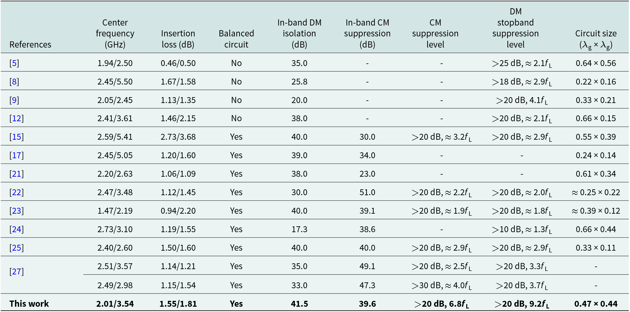
As shown in Fig. 14(a) and 14(b), the measured center frequencies for the lower and higher channels are 2.01 GHz and 3.54 GHz, respectively. The corresponding in-band minimum insertion losses are 1.55 dB and 1.81 dB, while the 3-dB FBWs are 7.4% and 8.1%. Transmission zeros near the passband are observed at 2.17 GHz and 3.73 GHz. It is also worth mentioning that 20-dB out-of-band suppression is achieved up to 18.5 GHz (9.2f L), featuring wide upper stopband responses. As depicted in Fig. 14(c) and 14(d), the in-band DM isolation exceeds 41.6 dB and 41.5 dB for the lower and higher channels, respectively. In the range of 0-18.5 GHz, the DM isolation exceeds 23.0 dB, while the CM isolation is better than 27.4 dB. As plotted in Fig. 14(e) and 14(f), the in-band CM suppression is greater than 44.1 dB and 39.6 dB for the lower and higher channels, respectively. Lower-channel CM suppression is better than 20 dB in the 0–13.7 GHz (6.8f L) range, and higher-channel CM suppression is better than 20 dB in the 0–9.0 GHz (2.54f H) range. The discrepancy between simulated and measured results is mainly due to the fabrication tolerances, the substrate characteristic instability, and the impedance mismatch between the SMA connectors and the PCB circuit at high frequencies.
Table 2 provides performance comparisons with previous works. As shown in Table 2, the proposed balanced diplexer exhibits a wide stopband and excellent CM suppression, which indicates that it has strong immunity to noise interference. Furthermore, the high DM isolation significantly reduces inter-channel crosstalk.
Performance comparisons with previous works

Conclusion
In this paper, a novel planar balanced-to-balanced diplexer with high isolation and harmonic suppression, designed using SIRs and UIR, is presented. While utilizing cross-coupling between SIRs to introduce transmission zeros, the impedance ratio of SIRs is flexibly adjusted to effectively suppress harmonics. Moreover, the theory and design methodology for the proposed diplexer are thoroughly analyzed. A microstrip prototype was designed and fabricated based on this method. The measured results demonstrate that the balanced diplexer features excellent CM suppression, a wide stopband, and high isolation. Therefore, the proposed balanced diplexer has a good potential to be applied to dual-channel two-way balanced communication systems [Reference Wei, Cheng, Liu and Shi24].
Acknowledgment
This work was supported by the National Natural Science Foundation of China (No. 61871417), the Natural Science Foundation of Liaoning Province (No. 2025-MSLH-097), the Basic Research Project of the Department of Education of Liaoning Province for Universities (No. LJ212410151023), the Liaoning Revitalization Talents Program (No. XLYC2007024), and the Fundamental Research Funds for the Central Universities (No. 3132025252).
Competing Interests
The authors report no conflict of interest.

Changqing Geng received the B.Eng. degree in communication engineering from Dalian Minzu University, China, in 2023. He is currently working toward the M.Eng degree in communication engineering at Dalian Maritime University (DMU). His current research interests include balanced components and diplexers.

Zhongbao Wang received the Ph.D. degree in communication and information systems from DMU, China, in 2012. He is currently a Full Professor with the School of Information Science and Technology, DMU. From 2014 to 2018, he was a Postdoctoral Fellow with Beijing University of Posts and Telecommunications, China. From 2019 to 2020, he was a Visiting Scholar with National University of Singapore, Singapore. He has authored more than 150 journal papers. He is currently serving as a Technical Reviewer for the IEEE Trans. on Circuits and Systems, MTT, MWTL, MOTL, and so on. His current research interests include balanced RF components and filtering antennas.

Dehao Zhao received the Ph.D. degree in electronic science and technology from Beijing Institute of Technology, China, in 2024. He is currently a Lecturer with the School of Information Science and Technology, DMU. He current research interests include multi-functional microwave devices and spatio-temporal modulation technology.

Hongmei Liu received the Ph.D. degree in communication and information systems from DMU, China, in 2016. She is currently a Full Professor with the School of Information Science and Technology, DMU. Her current research interests include passive microwave circuits, reconfigurable RF components, and CP microwave antennas.

Shaojun Fang received the Ph.D. degree in communication and information systems from DMU, China, in 2001. Since 1982, he has been at DMU, where he is currently the Head Professor with the School of Information Science and Technology. He has authored or co-authored four books and over 120 journal and conference papers. His recent research interests include passive RF components and antennas.