I. INTRODUCTION
Irradiation of crystalline solids leads to the formation of vacancy and interstitial clusters, both by direct condensation out of collision cascadesReference Voskoboinikov, Osetsky and Bacon1 and by aggregation of isolated point defects.Reference Kiritani and Takata2 Implanted gasses such as helium may further stabilize incipient void nucleiReference Ullmaier3–Reference Foreman and Singh6 and accelerate swelling.Reference Stoller and Odette7, Reference Odette8 As defect clusters form, the irradiated material hardens and may become brittle.Reference Odette and Lucas9 The formation of He bubbles and point defect clusters must, therefore, be curtailed in structural materials engineered for service in high radiation environments, such as nuclear reactors.Reference Roberto and Diaz de la Rubia10 One way to achieve this goal is to synthesize materials containing defect sinks that remove irradiation-induced point defects before they aggregate into clusters.Reference Odette and Stoller11–Reference Singh13
A defect sink whose effect on radiation response has been extensively studied is grain boundaries (GBs). Singh recognized that radiation-induced damage decreases with grain size because of the trapping of defects at GBs in a study on austenitic stainless steels.Reference Singh13 Similar observations have since been made in other polycrystalline materials, both metalReference Rose, Balogh and Hahn14–Reference Nita, Schaeublin, Victoria and Valiev16 and ceramic,Reference Rose, Balogh and Hahn14, Reference Nita, Schaeublin, Victoria and Valiev16 suggesting that it may be possible to markedly improve the radiation resistance of many materials by synthesizing them in nanocrystalline form. Atomistic modeling has confirmed the role of GBs in removing collision cascade-induced point defects and defect clusters in both fcc and bcc metals.Reference Samaras, Derlet, Van Swygenhoven and Victoria17–Reference Bai, Voter, Hoagland, Nastasi and Uberuaga20
Recent studies on Cu-Nb multilayered composites have demonstrated that heterophase interfaces also act as excellent point defect sinks: markedly fewer defect clusters form in these materials than in pure Cu or Nb under identical ion bombardment conditions.Reference Hochbauer, Misra, Hattar and Hoagland21–Reference Misra, Demkowicz, Zhang and Hoagland23 This difference arises from the presence of a large volume fraction of semicoherent interfaces in the Cu-Nb nanocomposites. Because point defect formation energies are an order of magnitude lower and rates of interfacial Frenkel pair annihilation are significantly higher at these interfaces than in the neighboring crystalline layers, Cu-Nb interfaces act as “super sinks” for irradiation-induced point defects, trapping and recombining them before defect clustering can take place.Reference Demkowicz and Hoagland24–Reference Demkowicz, Wang, Hoagland and Hirth26
The ultra-high mechanical strengthReference Misra and Hoagland27, Reference Mara, Bhattacharyya, Dickerson, Hoagland and Misra28 and morphological and chemical stability ofReference Misra and Hoagland29, Reference Misra, Hoagland and Kung30 Cu-Nb nanocomposites further indicate that structural nanocomposite materials could be designed to exhibit both high strengths and high radiation damage tolerance. Although most nanostructured materials exhibit high strengths,Reference Argon and Yip31 it is not clear whether all interfaces and GBs will exhibit “super sink” behavior for irradiation-induced point defects and He atoms.
Earlier studies tended to treat most GBs as perfect point defect sinks. Threshold stresses in Nabarro–Herring creep provided the earliest indication that point defect sink/source strengths may depend on GB structure.Reference Ashby32 More direct confirmation of such dependence was obtained by measuring the widths of zones denuded of vacancy clusters near different types of GBs in metals that were irradiated or quenched from high temperatures. Zone widths of 0.5–2 μm were found,Reference Siegel, Chang and Balluffi33–Reference Dollar and Gleiter35 indicating some variability in GB sink/source efficiency. Sink/source strengths of coherent boundaries were consistently low. Other studies have investigated the effect of GB structure on He trapping.Reference Lane and Goodhew36–Reference Thorsen, Bilde-Sorensen and Singh39 In most of these studies, however, full descriptions of GB crystallography were not given, and correlations with available parameters were qualitative at best. Atomistic modeling has revealed marked variability in the structures and behaviors of point defects absorbed at different types of GBs, different locations within individual GBs,Reference Sorensen, Mishin and Voter40–Reference Seki, Seidman, Oh and Foiles44 and individual GBs at different temperatures.Reference Seki, Seidman, Oh and Foiles43–Reference Kwok, Ho and Yip46
We hypothesize that interfaces that have atomic structures such that defect formation energies are low and Frenkel pair annihilation rates are high will be good sinks for radiation-induced point defects. Conversely, interfaces where point defect formation energies and Frenkel pair annihilation rates are comparable to those in the neighboring crystalline material are not expected to reduce irradiation-induced defect cluster formation. To test this idea on a simple, well-controlled example, we performed a coupled experimental/modeling study of the response of nanotwinned Cu (nt-Cu) samples, which contain large volume fractions of ∑3 symmetric tilt (i.e., ∑3 twin) boundaries, to high dose He implantation. These boundaries are coherent, i.e., they have perfect atomic registry between the neighboring crystals and are, therefore, fundamentally different from semi-coherent Cu-Nb interfaces which, like many general GBs, exhibit multiple atomic arrangements, a high density of misfit compensating defects, and excess atomic volume.Reference Demkowicz, Hoagland and Hirth25, Reference Suzuki and Mishin41
II. ATOMISTIC MODELING
Point defect properties near ∑3 twin boundaries in Cu were studied using atomistic simulations. Interatomic forces were modeled using the embedded-atom methodReference Daw and Baskes47 potential for Cu according to Voter,Reference Voter48, Reference Voter, Westbrook and Fleischer49 which has been shown to accurately reproduce the properties of point defects.Reference Mishin, Mehl, Papaconstantopoulos, Voter and Kress50, Reference Demkowicz and Hoagland51 He impurities were modeled using a recently developed predictive Cu–He pair potential.Reference Kashinath and Demkowicz52 A 29760 atom model containing two identical ∑3 twin boundaries was created by joining two appropriately oriented Cu crystals under periodic boundary conditions in all three directions. Each crystal consisted of 31 fcc {111} planes stacked parallel to the boundaries, giving a total thickness per crystal of 6.47 nm. The dimensions in the boundary planes were 5.11 nm in the <110> direction and 5.31 nm in the <112> direction. Atomic positions and model dimensions were relaxed by conjugate gradient energy minimization until the force acting on any atom did not exceed 1.6 pN and no stress component exceeded 0.01 MPa. The potential we used gives a twin boundary energy of 18.2 mJ/m2, in good agreement with the experimentally measured value of ∼20 mJ/m2.Reference Murr53
Vacancies were created in the relaxed model by removing atoms from their lattice positions. Self-interstitials and He impurities near Cu atoms with fcc environments were created in the tetrahedral, octahedral, crowdion, as well as <100>, <110>, and <111> dumbbell configurations.Reference Ehrhart and Ullmaier54 At each ∑3 twin boundary, there exists one close-packed plane of atoms with hcp environments. Near these atoms, interstitials were created in configurations characteristic of hcp crystals: tetrahedral, octahedral, crowdion, basal crowdion, tetrahedral and octahedral projections on the basal plane, c-dumbbell, and  and
 dumbbells.Reference Ehrhart and Ullmaier54, Reference Domain and Legris55 Each point defect was relaxed by conjugate gradient energy minimization, giving an atomic configuration corresponding to T = 0 K conditions.
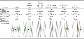
Table 1 lists point defect properties as a function of distance from a twin boundary. Defect properties in hcp Cu are also listed for reference. All defect properties from the third fcc {111} plane away from the boundary and onward are identical to those found in pure fcc Cu. Thus, the lowest energy self-interstitial configuration far from the twin boundary is the <100> dumbbell.Reference Mishin, Mehl, Papaconstantopoulos, Voter and Kress50, Reference Ehrhart56 It is also the one with lowest energy up to the fcc {111} plane immediately adjacent to the twin boundary. Between this plane and the boundary, the lowest-energy stable self-interstitial occurs at an octahedral site.
Properties of vacancies, He impurities, and self-interstitials as a function of location relative to a ∑3 twin boundary and in hcp Cu. In the visualizations, sites where creation of a vacancy leads to spontaneous recombination are shown in green. Interstitial atoms are red, boundary atoms orange, and fcc (and bulk hcp) Cu atoms blue.

Within the twin boundary itself, the lowest-energy self-interstitial is a dumbbell oriented along a <155> direction with respect to one of the two fcc lattices and, equivalently, along a <711> direction with respect to the other. In the hcp basis, this direction is within 3.4° of the  direction assuming an ideal c/a ratio and coincides perfectly with
 when the c/a ratio is 9/8 times the ideal ratio. Split dumbbell interstitials of this type have been previously considered in studies of magnetic relaxation in electron-irradiated Co.Reference Schaefer and Dander57 All lowest energy He interstitials near the boundary are of the octahedral type and have energies close to those of He octahedrals in fcc Cu. The lack of sites with high He binding energies can be attributed to the low excess volume of the ∑3 twin boundary.
For both vacancies and interstitials, the lowest formation energies are found in the fcc {111} plane immediately adjacent to the twin boundary, while the highest ones are found in the twin boundary plane itself. In all cases, the relative differences between these extremal values and the formation energies of the corresponding defects in pure fcc Cu do not exceed 2.2%. These results agree with previous studies where ∑3 twin boundaries were found to be essentially equivalent to fcc Cu from the standpoint of point defect formation energiesReference Suzuki and Mishin41 and confirm that these boundaries cannot serve as sinks for irradiation-induced defects. By contrast, point defect formation energies in incoherent Cu GBs (including incoherent ∑3 boundaries) and heterophase interfaces like those found in Cu-Nb multilayers may be as much as an order of magnitude lower than in the neighboring crystal layers.Reference Demkowicz, Hoagland and Hirth25, Reference Suzuki and Mishin41 Indeed, ∑3 twin boundaries seem to be unique among Cu GBs, in that their self-interstitial formation energies are not markedly different from those of fcc Cu.
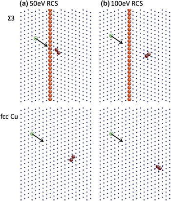
Furthermore, unlike some other symmetrical GBs,Reference Perez-Perez and Smith58 ∑3 twin boundaries in Cu seem to have only a minor effect on replacement collision sequences (RCSs). Figure 1 shows vacancy–interstitial pairs created by 50 and 100 eV RCSs along〈110〉-type directions in perfect fcc Cu and in the vicinity of a ∑3 twin boundary, both initiated in systems at T = 100 K. The ∑3 twin boundary does not arrest the RCSs: it only reduces the final separation of the defect pair. This lack of influence arises because the crystallographic tilt across the boundary, although significant at 60°, incidentally brings pairs of〈110〉-type directions from opposite sides of the boundary to within ∼30° of perfect alignment.
Vacancy-interstitial pairs produced by (a) 50 eV and (b) 100 eV replacement collision sequences (RCSs) across ∑3 twin boundaries and in fcc Cu. Vacancies are green, interstitial atoms are red, boundary atoms are orange, and fcc Cu atoms are blue. Arrows indicate RCS directions.

The rate of Frenkel pair annihilation is a much more difficult quantity to calculate than defect formation energies. It is known to be temperature dependentReference Dettmann, Leibfried and Schroeder59–Reference Wolfer and Si-Ahmed62 and likely involves contributions from interstitial configurations other than just the lowest energy ones.Reference Kidson63 A qualitative comparison of annihilation rates for different defect locations, however, can be obtained by measuring the volume of material in the vicinity of an interstitial where introduction of a vacancy leads to spontaneous recombination of the resulting Frenkel pair.Reference Grant, Harder and Bacon64 The larger this volume is, the higher the expected recombination rate will be.
We measure this volume by the number of atomic sites N recombine, where introduction of a vacancy leads to spontaneous recombination. For example, if recombination took place only if a vacancy was in a nearest neighbor location with respect to an interstitial, then the value of N recombine in an fcc crystal should be 12. The fact that N recombine is larger than 12 demonstrates that recombination can also occur for some non-nearest neighbor locations of vacancies and interstitials. The higher N recombine is, the more non-nearest neighbor recombination configurations a vacancy and interstitial have.
N recombine is listed in Fig. 1 along with the maximum vacancy–interstitial separation  at which the recombination occurs. Unlike defect formation energies, N recombine and
 in the vicinity of a ∑3 twin boundary are considerably larger than in fcc Cu. Thus, ∑3 twin boundaries may act as catalysts for enhanced Frenkel pair recombination. N recombine and
 at the ∑3 twin boundary are comparable, however, to the values obtained for hcp Cu. Thus, the differences in Frenkel pair recombination in fcc Cu versus a ∑3 twin boundary may arise from the local hcp structure of the atoms at the boundary.
The increased defect recombination range at ∑3 twin boundaries appears to affect the efficiency of Frenkel pair production from collision cascades. To model the effect of 33 keV He+ implantation (corresponding to the experimental conditions used in this study, as described in Sec. III), we performed collision cascade simulations in systems initially at T = 300 K, taking primary knock-on atom (PKA) energies between 0.5 and 2.5 keV with 0.5 keV increments.Reference Demkowicz and Hoagland51 This spectrum of PKA energies was chosen after calculating the means and standard deviations of energies transferred in collisions between 33 keV He and Cu using SRIM Monte Carlo simulations.Reference Ziegler, Biersack and Littmark65 For high impact parameter (recoil) collisions, the mean energy transferred is 230 eV with a standard deviation of 560 eV. Low impact parameter (replacement) collisions are about one-fifth as likely as recoil collisions, but the mean and standard deviation of energy transferred in them are 700 and 1070 eV, respectively.
The energy range we selected, therefore, probes within nearly two standard deviations of the mean PKA energy in replacement collisions. As 0.5 keV PKAs typically produced only one or two Frenkel pairs in our simulations, lower PKA energies were not modeled. The maximum (backscattering) energy that can be transferred to Cu by 33 keV He is 7.4 keV, but because this value lies over six standard deviations beyond the mean transferred energies for replacement collisions, such high energy PKAs are extremely rare and, therefore, also were not modeled.
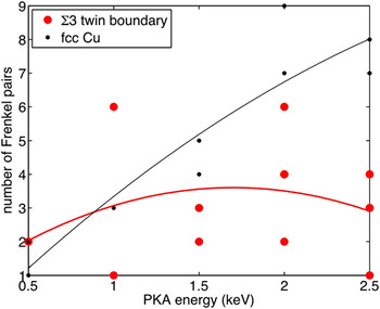
PKAs were chosen at distances of 0.3 and 2.4 nm from the boundary. Knock-on directions were chosen normal to the boundary with a superimposed random deviation not exceeding 5°. Four cascades were performed for 2.0 and 2.5 keV PKAs and two for each of the remaining energies. The number of Frenkel pairs produced as a function of PKA energy for all the simulations are compared to the corresponding number for pure fcc Cu in Fig. 2. At the higher PKA energies, there is a noticeable reduction in defect production efficiency near the twin boundaries compared to fcc Cu. This difference may be caused by enhanced in-cascade recombination owing to the increased recombination range at ∑3 twin boundaries.
Frenkel pair production efficiency in collision cascades with PKA energies above 2 keV is lower near ∑3 twin boundaries than in fcc Cu. Lines are quadratic least square fits to the defect creation data, provided as guides to the eye.

A simple estimate of the interaction between ∑3 twin boundaries and He bubbles was made by comparing the energies of He-filled bubbles located at such a boundary with ones in fcc Cu. Following Uberuaga et al.,Reference Uberuaga, Hoagland, Voter and Valone66 we investigated bubbles composed of 20 vacancies, which are ∼1 nm in diameter, containing either 10 or 20 He atoms. Averaging bubble energies in constant temperature and pressure simulations conducted at T = 300 K and P = 0 Pa over 0.5 ns, we found that the bubble with 10 He atoms was bound to the boundary with an energy of ∼0.1 eV while that with 20 He atoms was bound with an energy of ∼0.08 eV. These values are in excellent agreement with a computed ∼0.1 eV reduction in energy due to the removal of an amount of twin boundary area (with energy of 20 mJ/m2) equivalent to the equatorial cross-section of a 1-nm-diameter bubble. We, therefore, expect that at room temperature some He bubbles may be bound to ∑3 twin boundaries, albeit weakly.
III. He IMPLANTATION STUDY
The effect of ∑3 twin boundaries on the radiation response of Cu was investigated in He implantation experiments on nt-Cu films. Samples with a total thickness of ∼1.5 μm were grown epitaxially on a 10% HF-etched Si (110) substrate using magnetron sputtering at a deposition rate of ∼0.9 nm/s.Reference Anderoglu, Misra, Wang, Ronning, Hundley and Zhang67 The chamber was evacuated to a base pressure of 92 × 10−7 Torr before deposition. No heating or cooling was applied to the substrate during deposition. The Cu film is composed of columnar grains 70–150 nm in diameter. Because of the high deposition rate and low stacking fault energy of Cu,Reference Zhang, Wang, Chen, Lu, Lu, Hoagland and Misra68–Reference Zhang, Misra, Wang, Shen, Nastasi, Mitchell, Hirth, Hoagland and Embury72 numerous growth twins form in each columnar grain under these conditions.
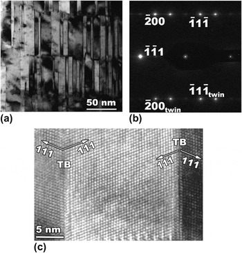
The cross-section TEM micrograph in Fig. 3 shows the microstructure of as-deposited nt-Cu. Distinct spots in the selected-area diffraction pattern confirm epitaxial growth. The average thickness of the twinned layers—and thus the average distance between twin boundaries—is 16 ± 0.5 nm. Because of the low energy of twin boundaries in Cu,Reference Murr53 this microstructure is thermally stable even up to T = 800 K (homologous temperature of T/T m = 0.75).Reference Anderoglu, Misra, Wang and Zhang73
Cross-sectional view of as-deposited Cu film showing nanometer-scale twins: (a) bright field TEM image, (b) selected area diffraction pattern corresponding to the image in (a) showing matrix and twin spots, (c) high-resolution TEM image showing that the twin boundaries oriented vertical in (a) are ∑3{111}.

Two room-temperature implantations with 33 keV He+ ions were carried out on as-deposited nt-Cu films. The first was on a sample with 70-nm-diameter columnar grains and was performed to a dose of 1016 ions/cm2 over a period of 15 min. The second was on a sample with 150-nm-diameter columnar grains to a dose of 1017 ions/cm2 over 180 min. The direction of ion flux was nearly normal to the twin boundaries: the samples were tilted by ∼5° from the beam direction to prevent channeling. Beam uniformity across the implanted area was confirmed by current measurements in four Faraday cups placed on the edges of the sample. Ion beam–induced heating was monitored using a K-type thermocouple placed within the implanted area and never exceeded 28 K.
During implantation, part of the nt-Cu film was masked (with an SS clip) and not exposed to irradiation. The boundary between the irradiated and unexposed region was scanned by an Ambios XP-1 profilometer and a step of ∼15 nm was detected. As no contamination from the chamber was seen on the surface of the samples, this finding indicates that swelling occurred in the implanted area of the film. He concentrations and displacements per atom (DPA) for the implantation conditions used in this study were obtained as a function of depth beneath the sample surface using the SRIM Monte Carlo code.Reference Ziegler, Biersack and Littmark65
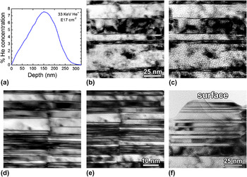
As-deposited and He-implanted nt-Cu films were examined by cross-sectional transmission electron microscopy using a JEOL 3000F microscope operating at 300 kV and by plan view scanning electron microscopy using an FEI Quanta 400F microscope. XTEM samples were mechanically polished down to ∼20 μm and then ion-milled and polished with energies of 5 and 2.5 keV, respectively. Care was taken to minimize sample heating during preparation of the TEM foils. No microstructure coarsening or twin boundary migration was observed. The implantation reaches a maximum depth of ∼300 nm and covers 18 ∑3 twin boundaries on average. A maximum implanted He concentration of about 7.5 at.% occurs at a depth of ∼150 nm.
Figure 4 compares near-focus and under-focused TEM images of the nt-Cu sample He-implanted with a dose of 1017 ions/cm2 at three different depths below the surface: 150 nm (peak He concentration), 400 nm (beyond the maximum range of implanted He), and the near-surface region. He bubbles are ∼1–2 nm in diameter and their distribution appears to correlate well with the implanted He concentration. Bubbles can be seen throughout the entire implanted region, including within 2–5 nm of the sample surface, even in the samples implanted to the lower dose of 1016 ions/cm2. This finding is consistent with the immeasurably small solubility of He in fcc Cu. The number of bubbles per unit volume appears to be greatest in the region of highest He concentration and decreases close to the maximum implantation depth. When bubbles are observed, they are so numerous that multiple bubbles are likely overlapping in the field of view and a reliable quantitative estimate of their concentration cannot be made. It is clear, however, that there are no He bubbles beneath the depth of 300 nm.
(a) Depth profile of He concentration in nt-Cu film implanted to a dose of 1017 ions/cm−2 with 33 keV He+ ions, calculated using SRIM. (b) Near-focus and (c) under-focused (−2 μm) bright field TEM images from a depth of 150 nm (peak He concentration). He bubbles appear as white dots in (c). Note the lack of any “bubble denuded zones” at boundaries. (d) Near-focus and (e) under-focused (−2 μm) bright field TEM images from a depth of 400 nm (below the He ion range). No bubbles are detected. (f) Under-focused (−2 μm) bright field TEM image from near surface. Note the presence of bubbles in spite of the very low He concentration.

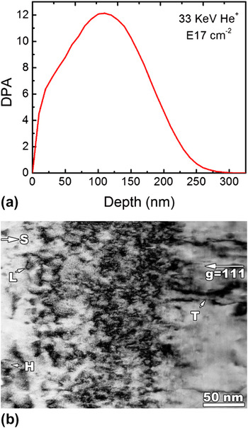
Figure 5 shows the same sample as in Fig. 4, but tilted into a two-beam condition, allowing dislocation loop defect clusters to be seen. The number per unit volume of dislocation loops correlates better with the DPA depth profile, shown in Fig. 5(a), than with the implanted He concentration, shown in Fig. 4(a). No dislocation loops are seen below a depth of ∼275 nm. The dislocations seen below 300 nm are threading dislocations: they span through the film thickness and result from island growth during deposition.
(a) Profile of displacements-per-atom (DPA) in nt-Cu film implanted to a dose of 1017 ions/cm−2 with 33 keV He+ ions, calculated using SRIM. (b) Diffraction contrast bright field TEM image. As the diffraction vector is normal to the twin boundaries, the contrast from the twin boundaries is very weak in this image. In (b), S, marks a point 50 nm below the film surface, T marks threading dislocations from growth, L are dislocation loops produced by He ion irradiation, and H are He bubbles. Note the lack of L and H below ≈250 nm as expected from the DPA and He concentration profiles, respectively.

The distributions of He bubbles and dislocation loops in nt-Cu are indistinguishable from those found in fcc Cu,Reference Hochbauer, Misra, Hattar and Hoagland21, Reference Zhang, Li, Anderoglu, Wang, Swadener, Hochbauer, Misra and Hoagland22 showing that ∑3 twin boundaries—even when present in high volume fractions and despite their potentially higher Frenkel pair recombination range—have negligible effect on the formation of radiation-induced defect clusters.
IV. DISCUSSION
We have shown that high volume fractions of ∑3 twin boundaries do not curtail the formation of vacancy and interstitial clusters in nanotwinned Cu subjected to high-dose He implantation. This observation is consistent with atomistic simulations, which show that these boundaries cannot act as effective defect sinks because their vacancy and interstitial formation energies are nearly identical to those of fcc Cu. It also agrees with previous studies, which failed to find denuded zones in the vicinity of ∑3 twin boundaries, even at elevated temperatures where defect mobilities are high.Reference Thorsen, Bilde-Sorensen and Singh38, Reference Thorsen, Bilde-Sorensen and Singh39 It may, therefore, be concluded that ∑3 twin boundaries are poor sinks for radiation-induced defects, in contrast to the heterophase interfaces found in Cu-Nb multilayer compositesReference Misra, Demkowicz, Zhang and Hoagland23 or certain high angle GBs, which reduce point defect concentrations in their vicinity even at room temperature.Reference King and Smith34
In contrast to studies conducted under neutron or electron irradiation,Reference Singh and Zinkle74, Reference Jager and Trinkaus75 we did not observe any stacking fault tetrahedra (SFTs). This finding agrees with previous experiments done using He ion implantationReference Hochbauer, Misra, Hattar and Hoagland21, Reference Zhang, Li, Anderoglu, Wang, Swadener, Hochbauer, Misra and Hoagland22, Reference Johnson and Mazey76–Reference Johnson, Thomson and Reader78 and is due to the fact that He prevents the collapse of vacancy clusters into dislocation loops or SFTs.Reference Zinkle, Wolfer, Kulcinski and Seitzman5, Reference Foreman and Singh6 Finely dispersed He bubbles may also serve as efficient sinks for any vacancies produced in the implantation process.Reference Odette and Stoller11
Previous studies on Cu implanted with He have reported the formation of ordered bubble lattices.Reference Johnson and Mazey76, Reference Johnson and Mazey77 Some indication was found that such superlattices may be forming over areas 20–30 nm in diameter in the near-surface regions of the nt-Cu samples we studied. This is surprising given that previous studies where such lattices have been observed were performed at He concentrations exceeding 10 at.%, i.e., considerably higher than those found in near-surface regions in our study. It is not clear to us at present whether ∑3 twin boundaries may aid in the formation of such superlattices.
The enhanced critical distances for Frenkel pair recombination in the vicinity of ∑3 twin boundaries did not have an appreciable impact on defect cluster formation. This is not surprising as their primary effect would be to lower defect production efficiencies in cascades with PKA energies above 2 keV. These, however, are comparatively rare under 33 keV He+ implantation, which produces far more PKAs of lower energy. Our results suggest, however, that it may be interesting to investigate the response of nt-Cu to high-energy, heavy ion bombardment, where the PKA energies are substantially higher.
We used a reaction-diffusion model to estimate what effect the increased recombination range would have in such investigations. In this model, the concentrations c v and c i of vacancies and interstitials in a perfect fcc Cu layer of thickness 10 nm bounded by twin boundaries are governed by the coupled equations
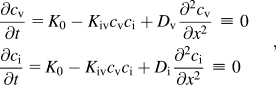
where K 0 is the Frenkel pair production rate, K iv is the Frenkel pair recombination rate coefficient, and D v and D i are vacancy and interstitial diffusivities. As the nt-Cu samples studied here are nearly free of in-grown dislocations, precipitates, and other potential point defect sinks, this system of equations is a reasonable description of defect concentration evolution before the formation of defect clusters (which are themselves sinks for radiation-induced point defects).
To model enhanced recombination and the associated reduced defect production at twin boundaries, K 0 and K iv were taken to be functions of position x normal to the boundaries,
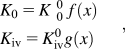
where f(x) and g(x) are shape functions. Because the defect recombination range peaks at the twin boundaries and decreases gradually as a function of distance away from them, we modeled g(x) as a shifted Gaussian centered on the boundaries:
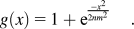
Equation (3) describes a boundary centered on x = 0 as a zone of thickness 1 nm at the center of which recombination is doubled. Choosing f(x) = 1/g(x), defect production at the boundary is halved by comparison to fcc Cu.
We solve the above model under the steady-state assumption, 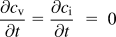 . In this case, the vacancy and interstitial concentrations are not independent, but rather must satisfy
 . We choose this constant to be
 , which describes defect concentrations that have equilibrated with a distant-free surface with thermal equilibrium values,
 and
 . The far-field defect production rate is
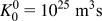 —a reasonable value for ion implantation experiments. Expressions for the remaining material parameters were evaluated as described in Ref. Reference Was79.
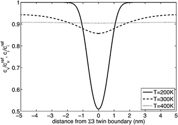
Figure 6 shows the computed steady state point defect concentrations for a single twin boundary bounded by 10 nm twins for three different temperatures (only half the twin thickness is shown on either side of the boundary). Defect concentrations c v and c i are scaled by the reference concentrations  and
 for pure fcc Cu (with no twin boundaries) under the same irradiation conditions. The most marked reduction of defect concentration occurs at the boundary at 200 K, when defect mobilities are least. This defect concentration is approximately proportional to the reduced defect production rate at the twin boundary and may lead to formation of smaller numbers of defect clusters at the boundary. At 400 K, defects are more mobile and there is a uniform ∼10% reduction in steady-state defect concentration by comparison to the reference values. Thus, a uniform defect cluster distribution may be expected at this temperature. Although the concentration of these defect clusters may be smaller in nt-Cu than in pure fcc Cu, the difference may be difficult to quantify reliably. Thus, it appears that heavy ion bombardment at cryogenic temperatures may be the best approach to verify the predicted reduced defect production rates at ∑3 twin boundaries.
Calculated vacancy and interstitial concentrations c v and c i (scaled by the reference concentrations  and
 in pure fcc Cu under the same irradiation conditions) near a ∑3 twin boundary. By comparison to fcc Cu, Frenkel pair recombination rates are double at the boundary and Frenkel pair production rates halved.

ACKNOWLEDGMENTS
The authors thank R.R. Greco for conducting the He implantations for this study. This research was funded by the LANL Directed Research and Development program. The replacement collision sequence, collision cascade, and reaction-diffusion modeling was supported by the U.S. Department of Energy, Office of Science, Office of Basic Energy Sciences under Award No. 2008LANL1026 through the Center for Materials at Irradiation and Mechanical Extremes, an Energy Frontier Research Center. XZ acknowledges financial support by NSF-DMR metallic materials and nanostructures program under Grant No. 0644835.