I. INTRODUCTION
Skutterudites show great promise for high-temperature thermoelectric (TE) applications as they possess a large unit cell, heavy constituent atoms, low differences in electronegativity of the constituent atoms, and large carrier mobility, which all are characteristics of a highly efficient TE material. In particular, filled skutterudites have been estimated as one of the prospective TE materials for power generation application and have been intensely studied for several decades.Reference Sales, Mandrus and Williams1, Reference Morelli, Meisner, Chen, Hu and Uher2 Various elements like alkaline earths,Reference Chen, Kawahara, Tang, Goto, Hirai, Dyck, Chen and Uher3, Reference Puyet, Lenoir, Dauscher, Dehmas, Stiewe and Mueller4 rare earths,Reference Nolas, Cohn and Slack5–Reference Kuznetsov, Kuznetsova and Rowe7 and others (Tl, Sn, and Ge)Reference Sales, Chakoumakos and Mandrus8–Reference Nolas, Yang and Takizawa10 have been used to fill the large voids in the crystal lattice to a varying degree in the CoSb3 framework.
TE conversion efficiency is determined by the dimensionless TE figure of merit ZT, which is defined as ZT = σS 2T/κ, where σ, S, T, and κ are the electrical conductivity, Seebeck coefficient, absolute temperature, and thermal conductivity, respectively. Ideally, a TE material possesses high electrical transport performance (high carrier mobility together with an optimized carrier concentration) and low thermal conductivity at the target operation temperature.
As demonstrated by He et al.Reference He, Chen, Rosenfeld and Subramanian11 and others,Reference Mallik, Stiewe, Karpinski, Hassdorf and Mueller12 indium-filled skutterudites are n-type semiconductors, which display high Seebeck coefficients and a maximum dimensionless TE ZT close to unity and above at elevated temperature. This suggests that indium-added cobalt–antimony skutterudites are among the most promising n-type TE materials. Additionally, it is assumed that nanoscopic impurity phases such as InSb have a further beneficial effect on the TE performance of CoSb3, which makes the In:CoSb3 system very appealing for further ZT enhancement of skutterudites.Reference Li, Tang, Zhang and Uher13
II. EXPERIMENTAL
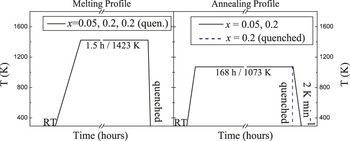
Specimens of indium-added cobalt–antimony-based skutterudites (InxCo4Sb12, with x = 0.05, 0.2) were prepared by inductive melting of the constituent elements in a sealed quartz ampoule. Stoichiometric quantities of In (6N; GoodFellow, London, UK), Co (3N; GoodFellow, London, UK), and Sb (6N; AlfaAesar, Ward Hill, MA) were melted for 1.5 h at 1423 K and subsequently quenched in a water bath to avoid peritectic decomposition of the skutterudite phase. Annealing was carried out in a programmable furnace at 1073 K for 168 h with a heating rate of 2 K min−1 from room temperature to 1073 K. For samples with the composition of In0.2Co4Sb12, two routes of cooling after the heat treatment were carried out to specifically affect the formation of the observed InSb/Sb precipitates. One sample was cooled down after annealing at a quite slow rate (2 K min−1), whereas the other was quenched in water after the holding time/plateau phase (Fig. 1). For easier distinction between the two samples with identical composition, the In0.2Co4Sb12 sample that was additionally quenched is marked with a superscript (In0.2Co4Sb12qu).
Melting and annealing profile of the synthesized material with x = 0.05, 0.2, and 0.2 (quenched).

Sample preparation for x-ray diffraction analysis (XRD) was accomplished by grinding a cross-sectional cutout of the as-cast cylindrical ingots. Crystallographic phases were analyzed using Cu Kα radiation (λ = 1.5406 Å) in Bragg–Brentano geometry with a graphite secondary monochromator from 2θ = 10°–80° with a step size of 0.02 deg and a scan rate of 500 s/deg. The lattice parameters were refined using the diffraction data (2θ = 10°–80°).
For scanning electron microscopy (SEM) analysis, a further cross-sectional sample from the ingot was embedded in a hot molding material containing graphite powder.
Specimens for transmission electron microscopy (TEM) examinations were obtained either by a cutout from the as-cast material (x = 0.05, 0.2) by a focused ion beam (FIB) or using finely ground powders of the as-cast material (x = 0.2). The specimens were examined in a Philips Tecnai F30 TEM (Philips, Amsterdam, Netherlands) operating at 300 keV and JEOL JEM 4100 (JEOL, Akishima, Tokyo, Japan) operating at 400 keV.
For powder compaction, direct current-assisted short-term sintering of the ground powders was performed under vacuum (10−2 mbar) in a 15-mm-diameter graphite die at 900 K and 50 MPa. Measurements of high-temperature Seebeck coefficient S and electrical conductivity σ were performed using temperature differential and 4-point probe methods with in-house-built measuring devices with an accuracy of 5% for S(T) and σ(T). The thermal conductivity κ was calculated from the thermal diffusivity D t measured by a laser flash analyzer (with an accuracy of 8%), specific heat c p confirmed by a differential scanning calorimeter (c p = 0.23 J g−1 K−1), and density ρ d using the relationship κ = D tc pρ d. The density was measured by the Archimedes method at room temperature.
III. RESULTS AND DISCUSSION
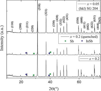
The XRD (Fig. 2) of ground material show the phase composition of the samples with an indium addition of x = 0.05 and x = 0.2. The sample with low indium content exhibits single phase skutterudite in contrast to material with x = 0.2, where InSb and Sb as secondary phases are becoming visible. The refined room temperature lattice parameter of the sample with x = 0.05 is a = 9.041 Å, for samples with x = 0.2 (In0.2Co4Sb12 and In0.2Co4Sb12qu) a = 9.048 Å. Comparing both x = 0.2 samples (i.e., In0.2Co4Sb12 and In0.2Co4Sb12qu), only minor distinctions can be located. The sample with a slow cooling rate after annealing seems to have higher crystallinity to some extent on the basis of the higher intensity of the diffractogram and higher amount of impurity phases.
X-ray powder diffractograms of indium-added skutterudites with x = 0.05 and x = 0.2. The strongest lines of the secondary phases are marked.

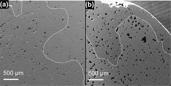
The cross-sectional SEM images in Fig. 3 of the as-cast samples with x = 0.05 and x = 0.2 show the porosity of the ingots, which was observed for all our synthesized material. Because of the long annealing step of 168 h at 1073 K, it is expected to have large grains of the skutterudite main phase, which were clearly visible.
SEM images (secondary electrons) of as-cast indium-added skutterudites with (a) x = 0.05 and (b) x = 0.2 at low magnification show the InxCo4Sb12 ingot comprising large grains (grain boundary marked with dotted line) and a porous structure.

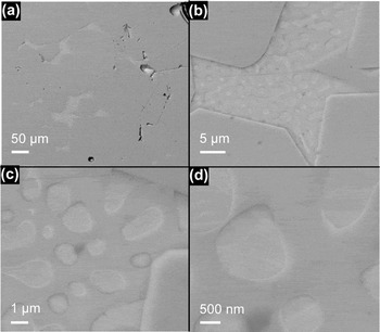
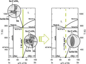
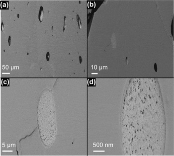
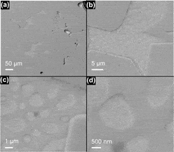
SEM evaluation of samples with x = 0.2 (Fig. 4) shows segregated secondary material exhibiting an internal structure at grain boundaries of the skutterudite phase, with a size of ∼10–50 μm. Accordingly, energy dispersive x-ray spectroscopy (EDX) data suggest that this impurity consists of almost pure Sb embedded in an InSb matrix. This microstructure can be explained by the InSb phase diagram at high Sb fraction (Fig. 5, left). In the annealing period at a temperature of 1073 K, minor amounts of Sb and In exist in the liquid state. During the slow cooling step of the In0.2Co4Sb12 sample, the In–Sb melt that has been separated between the grains reaches the L + Sb region of the phase diagram and the formation of Sb particles starts. During further cooling, these grow and the melt is depleted in Sb until InSb starts to solidify at the eutectic point, finally forming an InSb matrix enclosing almost separated pure Sb inclusions as a result of the very limited solubility of antimony in indium.
Scanning electron microscope (SEM) images (backscattered electrons) at (a, b) low and (c, d) high magnification of as-cast In0.2Co4Sb12 showing Sb precipitates in an InSb matrix at the grain boundaries of surrounding cobalt–antimony-based skutterudite domains.

InSb phase diagram and a possible formation mechanism of the observed microstructures in Fig. 4 and Fig. 6 (phase diagram fromReference Sales, Chakoumakos and Mandrus8).

From this consideration it is evident that the microstructure of the In–Sb precipitates in the In0.2Co4Sb12 material can be influenced by the cooling rate and to an extreme extent by quenching the sample after the heat treatment. Then the formation mechanism described in Fig. 5 (left) is disturbed as the system is lacking in time to reach equilibrium by diffusion and convection during the solidification period. In Fig. 6, it is observed that the size of the precipitates in the In0.2Co4Sb12qu sample was not markedly reduced, but the shape (almost elliptical after quenching) and substructure have changed considerably.
SEM images (backscattered electrons) at (a, b) low and (c, d) high magnification of as-cast In0.2Co4Sb12qu showing InSb + Sb mixture at the grain boundaries of surrounding cobalt–antimony-based skutterudite domains.

The micrographs show that because the cooling rate of In0.2Co4Sb12qu sample was enhanced, the formation of the previously mentioned nanometer-sized Sb precipitates was suppressed. Consequently, a much finer-scaled intermixture of InSb and Sb has been formed (Fig. 5, right).
EDX analysis of the precipitates reveals that these impurity phases consist of 72 at.% Sb and 28 at.% In, which is comparable with the gross composition InSb + Sb precipitates of the sample with similar nominal composition of In0.2Co4Sb12 but with a much slower cooling rate.
The occurrence of minor secondary phase areas in the microstructure of the samples with x = 0.2 is in good agreement with the XRD.
For x = 0.05, similar structures were not observed. This indicates that the solubility limit for indium in the skutterudite structure seems to be not yet reached. Moreover, no detectable impurity phases are found in the SEM at the composition of x = 0.05 as in the case of samples with x = 0.2. Considering that our synthesis is based on stoichiometric constituent elements, it suggests that indium can be incorporated in the skutterudite phase without forming detectable amounts of secondary phases. This can be attributed to the fact that indium possibly occupies vacant sites in the skutterudite lattice like the 2a Wyckoff position.Reference He, Chen, Rosenfeld and Subramanian11 However, it is noteworthy that with an indium addition of x = 0.2, proportions of pure antimony are found at the grain boundaries of the skutterudite phase, which is not the case for x = 0.05. Therefore, it is possible that indium atoms additionally can substitute the 24g Sb sites, like tinReference Grytsiv, Rogl, Berger, Paul, Bauer, Godart, Ni, Abd-Elmeguid, Saccone, Ferro and Kaczorowski14 in NiSb3 skutterudites, and entails a segregation of pure antimony out of the skutterudite phase because of stoichiometric reasons.
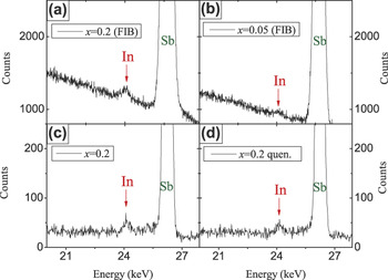
EDX measurements carried out in the TEM, making use of the In Kα-x-ray emission line at 24.139 keV, enabled us to detect an indium signal well separated from antimony or cobalt signals. Furthermore, with applying selected area electron diffraction (SAED) to the matrix range containing the In, we detected only the pure skutterudite phase. This leads us to the conclusion that indium is not only forming precipitates such as InSb but also incorporated to a large extent in the crystal lattice.
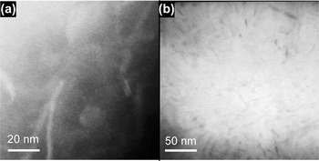
TEM images of samples made by FIB showed abundant appearance of rod-like precipitates (Fig. 7). The origin of these artifacts is presumably due to the heavy ion impact during FIB treatment and is in detail described and analyzed in one of our previous studies.Reference Sesselmann, Hassdorf, Kelm, Perlt and Mueller15 Further intensive study of these precipitates by scanning TEM (bright/dark field, high-angle annular dark-field imaging) and EDX mapping and high resolution TEM investigations brought no clear answer. However, these artifacts were not observed using a different sample preparation, where simply finely ground powder is placed on a holey carbon film supported by a copper grid. The comparison of the EDX spectra made from the FIB sample and the ground powder of the same as-cast material shows no significant distinctions.
Transmission electron microscope images of rod-like precipitates in CoSb3 skutterudite with different indium content. It was found that these precipitates do not represent an inherent nanostructure but are induced by sample preparation via focused ion beam (FIB); (a) x = 0.05 and (b) x = 0.2.

Figure 8 shows TEM–EDX spectra of indium-added skutterudite samples, which clearly exhibit a significant amount of indium incorporated in the skutterudite structure for x = 0.2 by means of the In Kα emission line at 24.14 keV, well separated from the Sb Kα emission line with an energy of 26.27 keV. Comparing both x = 0.2 samples (i.e., In0.2Co4Sb12 and In0.2Co4Sb12qu), no distinctions can be observed. For composition with x = 0.05, the In signal is due to the low concentration consequently too unincisive.
Energy dispersive x-ray spectra of indium-added skutterudite material (sample a and b are prepared by FIB, c and d by grinding of the as-cast material) with an indium content of x = 0.05, 0.2 (microstructure and selected area electron diffraction image at the measurement points reveal excellent crystallinity).

Microstructure and SAED images reveal excellent crystallinity at the measurement points. This leads to the assumption that indium is, to a large extent, incorporated in the skutterudite crystal structure and confirms, therefore, the results from the SEM evaluation.
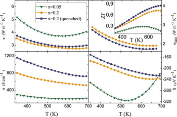
Figure 9 shows the thermal conductivity κ, the corresponding lattice thermal conductivity κ latt (for x = 0.2), the Seebeck coefficient S, the figure of merit ZT, and electrical conductivity σ as a function of temperature for short-term sintered InxCo4Sb12 (x = 0.05, 0.2) bulk materials, which had a relative density of at least 98%.
Temperature-dependent total thermal conductivity κ, corresponding lattice thermal conductivity κ latt, Seebeck coefficient S, electrical conductivity σ, and figure of merit ZT (inset diagram) of indium-added skutterudites with x = 0.05, 0.2; the addition “quenched” refers to a different thermal treatment of the material in the annealing process (Fig. 1).

The overall thermal conductivity ranged between 3.0 and 6.0 W m−1 K−1 and exhibits negative temperature dependence for both samples with x = 0.2. These specimens (In0.2Co4Sb12qu and In0.2Co4Sb12) have quite similar κ values under which In0.2Co4Sb12qu has a slightly higher overall thermal conductivity over the whole temperature regime. We applied the Wiedemann–Franz law κ el = L 0Tσ (L 0 = 2.45 ×∙−8 V−2 K−2) taking into account that κ = κ el + κ latt to ascertain whether the thermal lattice part κ latt of the overall thermal conductivity κ is suppressed by quenching after the annealing step or not. The lattice thermal-conductivity data show clearly that a reduction has been achieved. The higher overall thermal conductivity of the In0.2Co4Sb12qu material in comparison to In0.2Co4Sb12 is, therefore, caused by an increased electronic contribution of the total thermal conductivity κ.
For skutterudite material with low indium content of x = 0.05, the relatively high κ first decreases with rising temperature and increases again at about 550 K. This can be attributed to a bipolar conduction in the semiconductor, where the charge carriers of the valence band are thermally excited into the conduction band, and hence, the electronic thermal conductivity κ el is supplemented by a strong additional term for the thermal transport linked to the bipolar carrier flow.
The results from electrical conductivity measurements show that σ changes with variation of the indium content of the skutterudite material. However, the highest electrical conductivity is obtained for the In0.2Co4Sb12qu sample with 1200 S cm−1 at about 350 K and descends as a function of temperature, indicating a heavily doped semiconductor system. The sample In0.2Co4Sb12 shows similar temperature characteristics at a lower absolute value starting at 950 S cm−1 at about 350 K, whereas the sample with x = 0.05 displays a relatively low electrical conductivity and characteristics of beginning intrinsic semiconductor behavior at about 550 K, where the electrical conductivity of the sample increases again because of the bipolar conduction. This is compliant with the results on the thermal conductivity data.
Data from Seebeck coefficient measurements confirm that all synthesized short-term sintered samples show n-type behavior. The highest Seebeck coefficient in absolute values is obtained from the sample with the lowest indium content (x = 0.05). For samples with x = 0.2, it is notable that the quenched material has the lowest Seebeck coefficient of all and is considerably different from the slowly cooled sample with the same composition. Obviously, the quenched material has a higher carrier concentration than the latter. It has to be discussed what the effect of the cooling treatment on the carrier concentration of the skutterudite matrix could be. Either the real structure of the matrix itself is affected by quenching—it could be speculated that electrically active defects exist in the matrix at high temperature and are frozen during quenching instead of relaxing during slower cooling—or an interaction between the described In–Sb microinclusions and the matrix is taking place.
Consequently, indium as an addition to CoSb3 noticeably depresses the thermal conductivity κ and enhances the electrical conductivity, which yields to a ZT above 0.7 at 675 K for x = 0.2 (Fig. 9, inset top right). Notably, the quenched sample (In0.2Co4Sb12qu) shows higher ZT values because of the improved electrical conductivity in comparison to In0.2Co4Sb12.
The vastly reduced thermal conductivity of the material and the n-type behavior of the bulk material are further verifications that indium occupies mainly the 2a site of the skutterudite like the chemical-related thalliumReference Hermann, Jin, Schweika, Grandjean, Mandrus, Sales and Long16, Reference Harnwunggmoung, Kurosaki, Muta and Yamanaka17 and is not particularly substituting the Sb site that would probably lead to a p-type material.
Furthermore, minor changes in the synthesis parameter of the In:CoSb3 system during the annealing process suggest having a major influence on the electrical conductivity and lattice thermal conductivity of the bulk material. This strongly indicates that an optimized ZT of the In:CoSb3 system can only be achieved when the phase diagrams of possible secondary phases are considered. As a consequence, the TE properties of indium-added cobalt–antimony-based skutterudites may be deteriorated when the quenched material is again heated above the eutectic point of the In–Sb phase diagram.
IV. CONCLUSIONS
For the composition with x = 0.05, we synthesized phase pure skutterudites and with minor secondary phases in the case of x = 0.2. Synthesis of the as-cast material involved inductive melting of stochiometric fractions of constituent elements and subsequent long-term annealing at high temperature.
SEM analyses for material with x = 0.2 exhibit precipitates along the skutterudite grain boundaries consisting of nanometer-sized islands of almost pure Sb phase embedded in an InSb matrix. These precipitates can be considerably modified by specifically changing the cooling rate of the annealing process. In quenched material, we obtained elliptically shaped precipitates that consist of a diffusive intermixture of InSb and Sb. These formations and its microstructures of the secondary phases can be described by the In–Sb phase diagram at high Sb fraction. For the sample with x = 0.05, no such impurity phases were observed.
EDX together with TEM and SAED analysis reveals that indium is to a large extent incorporated in the skutterudite structure. Hence, it confirms our assumption that indium can occupy partly the 2a site in the skutterudite structure like the chemical-related thallium. Furthermore, the behavior of In may be alike to that of Sn in NiSb3 and, therefore, additionally substitute antimony sites (24g site) in the skutterudite phase because displaced portions of pure Sb are found at higher In concentration (x = 0.2), which is not expected for stochiometric reasons.
Transport properties of the short-term sintered bulk material showed that indium is improving the ZT, thereof the sample with In0.2Co4Sb12 shows highest ZT. Furthermore, minor changes in the synthesis parameter of the In:CoSb3 system during the annealing process suggest to have a major influence on the electrical conductivity and lattice thermal conductivity of the bulk material, and as a consequence, the ZT of In0.2Co4Sb12 could be further increased noticeably.
ACKNOWLEDGMENTS
The authors thank the Deutsche Forschungsgemeinschaft and the SPP1386 “Nanostrukturierte Thermoelektrika: Theorie, Modellsysteme und kontrollierte Synthese” for funding this research work at the German Aerospace Center (DLR), Cologne, Germany. We thank our cooperation partners, the group of Prof. S. Schlecht (University of Gießen) and the group of Prof. B. Paulus (FU Berlin) for helpful discussions.