I. INTRODUCTION
Over the past several years, although considerable efforts have been made on the synthesis of various nanostructures and thin films, particularly, significant breakthrough was in synthesizing boron nitride (BN) and zinc oxide (ZnO) nanostructures. BN is one of the most interesting nonoxide materials with a potentially bright future in advance material design. This material has great potential for the applications in high performance electronic devices, insulating nanotubular shields, hydrogen storage media, gas absorbents, and reinforcing agents. Like in the case of carbon, different types of BN nanostructures have been produced. Cho et al.Reference Cho, Kim, Kim, Park, Choi, Shin, Gao and Kang1 prepared BN nanotubes, Bernard et al.Reference Bernard, Salles, Foucaud and Miele2 synthesized and characterized nanoparticles and fullerenes, and very recently, Zhi et al.Reference Zhi, Bando, Tang, Kuwahara and Golberg3 and Lin et al.Reference Lin, Williams and Connell4,Reference Lin, Williams, Cao, Ali and Connell5 prepared exfoliated graphene-like BN nanosheets, and these inorganic sheets were utilized to improve thermal and mechanical properties of the polymeric composites. Meyer et al.Reference Meyer, Chuvilin, Algara-Siller, Biskupek and Kaiser6 synthesized the clean single-layer hexagonal boron nitride (h-BN) and reported atomic resolution imaging. Furthermore, BN polymers have been proposed as new building blocks for electronic devices. Based upon quantum-mechanical simulations, BN can be formulated to tune electronic properties. Such materials would be much cheaper than conventional semiconductors reported by Cote et al.Reference Cote, Haynes and Molteni7 On the other hand, ZnO has attracted considerable attention because of its low cost, nontoxicity, high stability, and high efficiency. Recently, much attention has been focused on growth and modification of ZnO nanostructures, such as nanowires and nanorods. Kyoungwon et al.Reference Kyoungwon, Yong-Won, Seongpil, In-Ho, Sangsig and Sang8 modified ZnO nanowires by doping or substituting with special atoms. However, for the industrial and fundamental practical applications, it is necessary to grow such materials on a large scale. So far, it is a challenging task to fabricate high purity mass product nanostructures and thin films on a large scale.
There exist techniques for the synthesis of nanostructured BN and ZnO, including arc discharges, laser ablation, ball-milling, plasma jet, and substitution reactions in chemical vapor deposition (CVD). Very recently, Song et al.Reference Song, Ci, Lu, Sorokin, Jin, Ni, Kvashnin, Kvashnin, Lou, Yakobson and Ajayan9 successfully used the CVD process to grow large BN sheets. Li et al.Reference Li, Liao, Zhang, Zhang, Zhu, Gao, Laurent, Leprince-Wang, Wang and Yu10 also synthesized n-type and p-type phosphorus-doped ZnO (ZnO:P) nanowires by the CVD method using phosphorus pentoxide (P2O5) as the dopant source. In most of the cases, the material growth rate is low and the material produced would unavoidably yield impurities in the samples. Therefore, to achieve high growth rate nanostructures and thin films, these synthesis techniques need to carry out at very high temperatures (1100–2700 °C) and high pressure. Moreover, using CVD method, the growth rate of ceramic materials particularly BN is much lower even if the deposition time is too long.Reference Wu, Qiao, Chong and Shen11,Reference Zhu, Wang, Holloway, Outlaw, Zhao, Hou, Shutthanandan and Manos12 On the other hand, pulsed laser deposition (PLD) has been regarded as a versatile method to grow ceramic thin films, such as BN and ZnO. The PLD technique seems to be economic and provides a quick method for the growth of nanostructures and thin films at comparatively low substrate temperatures and low pressure. It is conceptually a simple technique that generates reactive species of the target material under highly nonequilibrium conditions, which cannot be produced by any other technique. This leads the way to the growth of the materials having unique properties, and indeed, this technique proving to be one of the most attractive methods to synthesize high yield of thin films. One of the advantages of PLD is that it can largely avoid contamination because laser installed outside the chamber; consequently, operation of laser plasma deposition is much flexible. Here, we should also consider the critical role of carbon dioxide (CO2) in PLD. The CO2 laser produces radiations in the far infrared part of the spectrum. Light in this part of the spectrum generally produces a heating effect upon impact on the surface of the target material. It ablates the target material and produces plasma plume composed of reactive species of the material to be deposited. The geometry of plasma plume is cylindrical or spherical, which depends on the pressure inside the deposition chamber, and it is highly forward directed toward the substrate. This plasma plume can reach on the substrate surface and can deposit mass product nanostructures and thin films. Finally, the growth rate of the sample increases.
In our previous report, Feng et al.Reference Feng and Zhang13 synthesized various nanomaterials of carbon and carbon-related materials using an ArF Lambda Physics 1000 (Lambda Physik Inc, Ft. Lauderdale, FL) plasma deposition technique. However, due to the low power density of ArF Lambda excimer laser, it was difficult to increase the growth rate to obtain mass product nanostructures and thin films. Therefore, to increase the growth rate and achieve mass product nanomaterials, it was necessary to develop higher power laser plasma deposition systems. Herein, we report on the installation of CO2-PLD system and its application for the quick synthesis of various nanostructures and thin films. The growth rate in CO2-PLD increased by more than 10 times than that of an ArF Lambda laser machine. Moreover, within few minutes of the activation process, we achieved uniform deposition of materials on entire surfaces of the substrates.
II. EXPERIMENTAL WORK
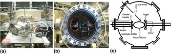
Figure 1(a) shows the photograph of the installed CO2-PLD system. Figure 1(b) shows the inside view of the chamber where different equipments are installed. The dimensions of the chamber and equipment used are indicated in the block diagram [Fig. 1(c)]. The designed components are listed as follows:
i. Heater and thermocouple for controlling temperature.
ii. Two-dimensional adjustable substrate holder with multi clamps used for holding 3–6 different substrates at the same time.
iii. Five-dimensional adjustable target holder together with the motor for controlling rotational velocity of target, direction, and location. The distance between the target and the substrate holder can be flexibly adjusted from 2 to 8 cm for controlling plasma density on the surface of the substrate that determines the growth rate.
iv. Shutter for blocking the plasma beam or impurities.
v. Three gas inlets and controllers for controlling types of gasses and gas pressure.
vi. Long focal length lens was selected so that we can install the lens outside the chamber to avoid it from plasma contamination. It is also noted that with longer focal lens, laser would produce a plasma beam with smaller spread angle.
vii. High power rotary pump and turbo molecular pump for controlling vacuum down to 10−7 Torr.
viii. Various power supplies.
ix. Three vacuum gauges used for detecting different ranges of vacuum in the chamber.
x. Several optical windows installed for characterizing the plasma.
(a) Photograph of the installed CO2-PLD system, (b) inside view of the deposition chamber and (c) schematic of the deposition chamber.

Most of the experiments were performed with the target to substrate distance ranging from 2 to 5 cm. The longer or shorter distance could be desired based on the fact that the deposition with laser plasma consists of two processes, ionic deposition and molecular deposition. If longer distance will be selected, it might be possible that boron and nitrogen ions recombine into molecules before reaching to the substrate surface that will affect the boron/nitrogen (B/N) ratio in the samples. Therefore, for the stoichiometric nanostructure growth process, a short distance is required for atomic deposition so that the B/N ratio could be equal or near to 1. Meanwhile, to control the growth rate and achieve large areas of the coated films, longer distance could be desired. For the case of higher beam energy, larger distance between the substrate and the target is necessary so that the high-energy plasma ions would not destroy the surface of the initially grown layers or nanostructures. This fact also been reported by Noorhana et al.Reference Noorhana, Beh and Mansor14 Considering all above parameters, we optimized the substrate to the target distance of 3 cm. It was noticed that tip of cylindrical plasma plume was lying directly on the surface of the substrate. In such way that uniform and optimized depositions could be possible.
The laser incident angle “θ” with respect to the target plane was set at 45°. This was because if the angle will be too small (close to grazing angle), the size and the location of the spot were difficult to be controlled. In contrast, if the angle is too large, the substrate holder will be an obstruction.
The new design of the substrate holder can easily hold multiple substrates. The manner in which the substrates were held and their location and orientation relative to the target were important parameters in the CO2-PLD system. We designed locally the substrate holder based on the ceramic cup. The base of the substrate holder was of molybdenum plate that screwed four metal clamps to hold the substrate in a vertical position directly facing the target. The purpose of the number of clamps was to place the different kind of substrates at the same time to study the effect of material on nanostructures under the same experimental conditions and environment. When the laser ablates the target, the evaporants eject a highly forward directed plume along the target normal. Therefore, the substrate must be held directly opposite to the target. The tungsten wire was used as a filament to heat the substrate and achieved the desired temperature during deposition. An aluminum plate was also inserted to cover the base port of the chamber (where a turbo pump was installed). The plate protects the turbo pump from any kind of contamination or piece fall down from the substrate holder, target, or from the chamber.
During the deposition process, the evaporants from the target moves to all surfaces within the chamber including the direction of laser window. Therefore, the material deposited on the window will interact with the laser beam resulting permanently damage to the window. Therefore, we adjusted the window to a target distance up to 25 cm such that the material reach to the window is to be greatly reduced.
Target was installed to easily access within the chamber so that mounting and demounting should be as simple as possible. To get uniform and large area deposition of the sample, a motor was connected to the target holder to rotate the target during deposition. In this manner, plasma plume produced on the surface of the target also rotates with the target and covers the entire substrate surface. Two special lenses were arranged one for focusing purpose and the other was used as the CO2 laser window so that the laser pulses hit the target accurately.
A series of experiments were conducted under different experimental conditions for the nucleation of nanostructured BN and ZnO. First experiment was performed using the h-BN target. The pressure inside the chamber was maintained at 4 × 10⁻⁶ Torr and the temperature of the substrate was kept at 300 °C. For the deposition of nanostructured BN, silicon (Si) and molybdenum (Mo) were selected as substrates and placed together on the substrate holder. In the 2nd set of experiment, an h-BN target was replaced with ZnO and two more experiments were performed individually at 300 °C and at 400 °C substrate temperature, respectively. For 2nd and 3rd experiments, Si was used as the substrate material. All other experimental parameters were kept the same. A CO2 laser with a wave length of 10.6 μm and the output power of 75 W were used to irradiate h-BN or ZnO targets. The repetition rate of the laser pulses was kept at 5 Hz. The laser beam was focused onto the target with a lens of 10 inch focal length, and an incident angle of 45° relative to the target surface. The square-shaped focused spot of laser beam onto the target was 1 mm. The power density of the laser on the target was 2 × 10⁸ W/cm2 per pulse. However, the average value of the power density is 2.5 × 10³ W/cm2. The distance between the substrate and the target was 3 cm. The duration for each deposition was kept for 5 min.
Prior to the deposition, Mo disks were polished with diamond powder (diameter <10 nm), cleaned with acetone and methanol, and then rinsed with deionized water in sequence to remove impurities. Whereas mirror polished commercial Si (100) wafers were directly used after cleaning with acetone to remove the subsequent oxygen layer from the surface.
The system (CO2-PLD) has been tested before its application. The best vacuum can be achieved down to 10−7 Torr, and the substrate temperature can be controlled up to (1 ± 10%) × 1000 °C. The motor was rotating with approximately 400 rotations per minute. The flow rate of the gas can be controlled up to 0.3 m3/h.
III. RESULTS AND DISCUSSION
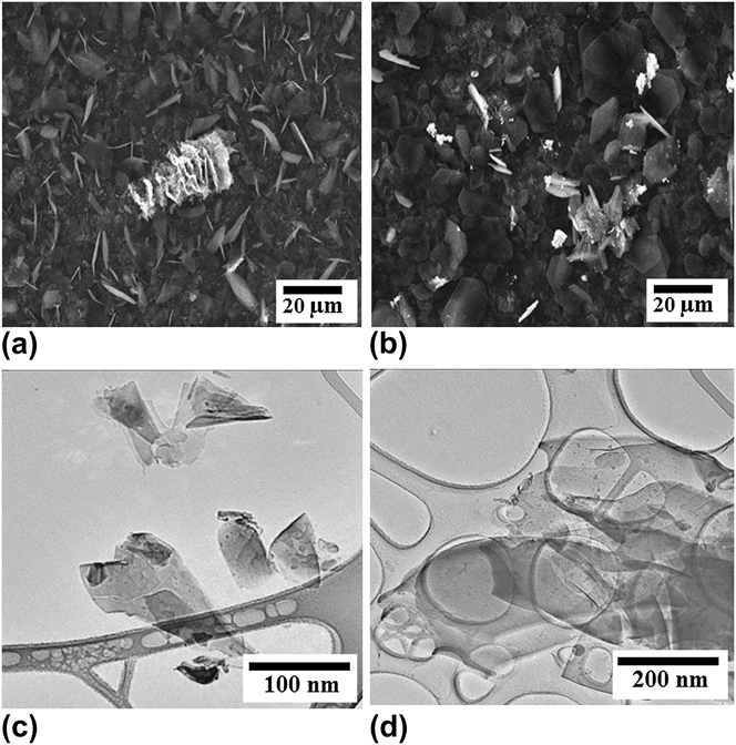
After test, CO2-PLD was used for the synthesis of various nanostructures. First experiment was performed using an h-BN target to deposit nanostructured BN on Mo and Si substrates. Top-view scanning electron microscopy (SEM) images recorded from the samples prepared on Mo and Si substrates shows that entire surfaces of the substrate are covered with large numbers of randomly oriented BN nanostructures (Fig. 2). The image recorded from the sample prepared on the Si substrate indicates cone- and ribbon-shaped nanostructures with average length of each continuous piece of ribbon or cone are around 20 μm [Fig. 2(a)]. The image recorded from the surface of Si substrates shows disk-shaped morphology [Fig. 2(b)]. The disks are further composed of several BN nanosheets. These sheets are smooth, flat, and transparent to the electron beam. Few small disks are visible underneath of the top ones further indicating the transparency of the samples. It is observed that nanostructures deposited on different substrates have different morphologies under the same experimental conditions applied. It could be possible that the formation of nanostructures may depend on the substrate material because of bonding made by deposited ions and atoms with subsequent surface atoms of the substrate. The observed differences could also be possible because of substrate structure effects, as substrate offers sites for homogeneous nucleation and mismatches of thermal expansion coefficients between the synthesized material and the substrate material.Reference Ljubica, Ljijana and Vladimir15 For more precise investigations of as grown nanostructures, transmission electron microscopy (TEM) measurements were conducted and results are presented in Figs. 2(c) and 2(d). TEM image of the sample grown on top of the Mo substrate is shown in Fig. 2(c). The Image shows several BN clusters of conical shaped as we observed before SEM measurements. However, at this stage, we can see more clearly that the samples are composed of layered structure.Reference Pakdel, Zhi, Bando, Nakayama and Golberg16 On the other hand, the sample grown on the Si substrate is composed of several thin films overlapped on the top of each other as shown in Fig. 2(d). Therefore, both from SEM and TEM measurements, we revealed that the sample consists of many overlapping sheet structures, indicating layered growth characteristics.
Top-view SEM micrographs of BN nanostructures synthesized on (a) Mo and (b) Si substrates, respectively. TEM images of the synthesized BN samples on (c) Mo and (d) Si substrates. The scale bars are shown on the images.
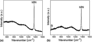
The crystalline structure of the samples was analyzed by Raman spectroscopy using a triple monochromator with an excitation wave length of 514 nm (Ar+ ion Laser). The microscope focused the laser beam on the surface of samples. Figure 3(a) shows the Raman spectrum recorded from BN samples deposited on the Mo substrate. A clear Raman active E 2g mode of the BN at ∼1365 cm−1 was identified, indicting the hexagonal phase in BN nanostructure.Reference Nemanich, Solin and Martin17–Reference Wu, Han, Walukiewicz, Ager, Shan, Haller and Zettl19 Almost a similar trend in the peak profile is observed from the Si substrate [Fig. 3(b)]. The extremely narrow Raman active E 2g peak probably suggests that the obtained sample has less defect concentrations. Compared with a traditional CVD method that in most cases yields high level of impurity inside the samples, the present plasma pulse beam deposition technique could produce high purity of BN nanostructures. No carbon and other impurities were detected.
Raman spectra of BN samples prepared on (a) Mo and (b) Si substrates, respectively.

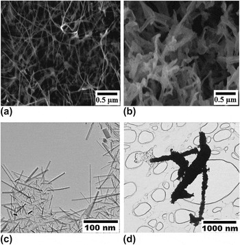
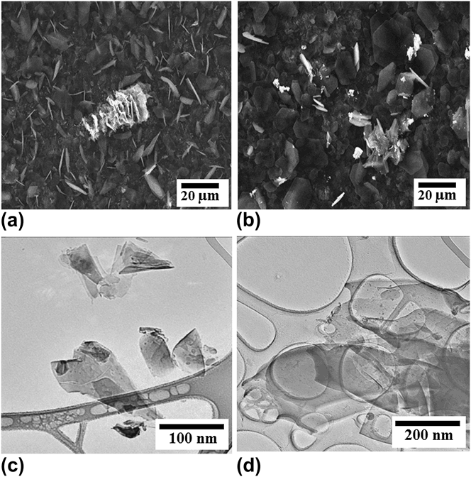
For further applications of the system, two more experiments were conducted using the ZnO target. The main focus of these experiments was to analyze the effect of substrate temperature on the growth of ZnO nanostructures. The surface morphology of ZnO nanostructures is studied with SEM and TEM measurements. Top-view SEM images of ZnO nanowires grown at 300 and 400 °C, respectively, are presented in Figs. 4(a) and 4(b), while Figs. 4(c) and 4(d) shows TEM images of the samples. The entire surface of the substrate was covered with randomly directed web-like nanowires with a mean diameter of about 10 nm and an average length of about 1 μm were obtained at 300 °C [Fig. 4(a)]. When ZnO nanowires were synthesized at 400 °C, the average diameter and length were estimated around 50 and 500 nm [Fig. 4(b)]. Therefore, it can be predicted that the temperature plays an important role on the morphology of the nanowires and the sample growth rate. TEM images [Figs. 4(a) and 4(c)] of ZnO samples are showing slightly different morphologies compared with SEM measurements. This difference is possibly due to the following factors: (i) SEM has limited resolution and shows number of condensed nanostructures, whereas TEM images have higher resolution compared with SEM and shows large and dispersed nanostructures. (ii) For TEM measurements, samples were scratched from the substrate surface to the TEM grid, and it could be possible that during the transfer process, samples dispersed and show slightly different morphologies. The general interpretation for the formation of nanostructures is that when laser impacts on the target material, it ablates the target surface and produces plasma composed of high-energy ions and clusters. When these ions and clusters land on the substrate surface, the extra thermal activation besides the substrate heating is provided to the sample by energy exchange through collisions between the active ions, clusters, or atoms. This helps to create small size crystallites that combine and form dense structure of nanowires.Reference Takahashi, Noguchi and Miyayama20–Reference Sajjad and Feng23 TEM results collected from ZnO samples are inconsistent with SEM measurements as shown in Figs. 4(c) and 4(d).
Top-view SEM images of ZnO nanowires grown on the Si substrate at (a) 300 °C and (b) 400 °C, respectively. TEM images of ZnO samples prepared at (c) 300 °C and (d) 400 °C, respectively. Scale bars shown on the images are 0.5 μm.

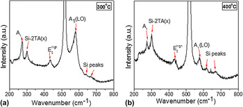
Figure 5 shows Raman measurements of ZnO nanostructures. Two optical modes of ZnO local at 434.1 and 578.9 cm−1 corresponding to  $E_2^{{\rm{\,high}}}$ and A 1 (LO), respectively, which was indicative of the wurtzite crystal structure of nanowires are shown in Fig. 5(a). Such peaks and crystalline structures were also identified by Yang et al.Reference Yang, Feng, Kumar, Katiyar and Achermann24,Reference Yang, Kumar, Feng and Katiyar25 These peaks were still visible when the temperature increases up to 400 °C [Fig. 5(b)]. Apart from the optical modes of vibrations of ZnO, four optical modes related to Si are also observed from both figures at 300.4 cm−1 [Si-2TA(X)], 518 cm−1 (Si), 618 cm−1 (Si- peaks), and 670 cm−1. Moreover, the mode A1 at a frequency of 273 cm−1 which was evidenced as local vibrational modes of N in ZnO was clearly observed. Such vibrational modes were also reported before by Koki et al.Reference Koki, Yasushi, Kouhei, Koichi, Kiyoshi, Makoto and Bao-Ping26 and Pan et al.Reference Pan, Song, Liu, Yang and Zeng27 When temperature was increased from 300 to 400 °C, the intensity of A1 was reduced below the intensity of Si-2TA(X), which indicates decreasing behavior of substitutional behavior of N3− for O2− as shown in Figs. 5(a) and 5(b).
Raman spectra of ZnO nanowires grown on the Si substrate at (a) 300 °C and (b) 400 °C, respectively.

IV. CONCLUSIONS
In summary, the CO2-PLD system can be used for the quick synthesis of high purity mass product nanostructures and thin films. The best vacuum of the system is achieved down to 10−7 Torr, and the substrate temperature is controlled up to (1 ± 10%) × 1000 °C. The rotation of the motor is up to 400 per minute. The distance between substrates and targets (3 cm) give rise to a uniform deposition of the nanostructures and thin films. The growth rate can also be achieved around 1 μm/min. Highly dense web-like ZnO nanowires and BN nanostructures can be achieved on the entire surface (2 × 2 cm2) of the substrates. From Raman results, it is concluded that deposited BN nanostructure has hexagonal phase dominating in the samples. Substrate temperature also plays a critical role for the formation of nanostructures that can be used for various fundamental and practical applications. The large-scale growth of other ceramic and semiconductor materials are under investigation.
ACKNOWLEDGMENTS
This work is partially supported by NSF-DMR (0706147). We would like to thank Dr. Carlos Cabrera and his staff for SEM measurements.